EP0484759B1 - A power controlling apparatus with a power failure detecting function - Google Patents
A power controlling apparatus with a power failure detecting function Download PDFInfo
- Publication number
- EP0484759B1 EP0484759B1 EP91118195A EP91118195A EP0484759B1 EP 0484759 B1 EP0484759 B1 EP 0484759B1 EP 91118195 A EP91118195 A EP 91118195A EP 91118195 A EP91118195 A EP 91118195A EP 0484759 B1 EP0484759 B1 EP 0484759B1
- Authority
- EP
- European Patent Office
- Prior art keywords
- failure
- blinker
- power source
- detecting
- bit
- Prior art date
- Legal status (The legal status is an assumption and is not a legal conclusion. Google has not performed a legal analysis and makes no representation as to the accuracy of the status listed.)
- Expired - Lifetime
Links
Images


Classifications
-
- G—PHYSICS
- G06—COMPUTING; CALCULATING OR COUNTING
- G06F—ELECTRIC DIGITAL DATA PROCESSING
- G06F1/00—Details not covered by groups G06F3/00 - G06F13/00 and G06F21/00
- G06F1/26—Power supply means, e.g. regulation thereof
- G06F1/28—Supervision thereof, e.g. detecting power-supply failure by out of limits supervision
-
- H—ELECTRICITY
- H02—GENERATION; CONVERSION OR DISTRIBUTION OF ELECTRIC POWER
- H02H—EMERGENCY PROTECTIVE CIRCUIT ARRANGEMENTS
- H02H3/00—Emergency protective circuit arrangements for automatic disconnection directly responsive to an undesired change from normal electric working condition with or without subsequent reconnection ; integrated protection
- H02H3/02—Details
- H02H3/04—Details with warning or supervision in addition to disconnection, e.g. for indicating that protective apparatus has functioned
- H02H3/042—Details with warning or supervision in addition to disconnection, e.g. for indicating that protective apparatus has functioned combined with means for locating the fault
-
- H—ELECTRICITY
- H02—GENERATION; CONVERSION OR DISTRIBUTION OF ELECTRIC POWER
- H02H—EMERGENCY PROTECTIVE CIRCUIT ARRANGEMENTS
- H02H3/00—Emergency protective circuit arrangements for automatic disconnection directly responsive to an undesired change from normal electric working condition with or without subsequent reconnection ; integrated protection
- H02H3/24—Emergency protective circuit arrangements for automatic disconnection directly responsive to an undesired change from normal electric working condition with or without subsequent reconnection ; integrated protection responsive to undervoltage or no-voltage
Definitions
- the present invention relates to a power controlling apparatus for detecting a power failure of a power source circuit, which is used in an electronic equipment such as a personal computer, and displaying detected results.
- an electronic equipment such as a personal computer uses as its power source a commercially available alternating current source (an AC source) or a chargeable battery (a chargeable internal battery). It uses a DC/DC converter, etc., to generate various direct currents, each having its own necessary voltage level (a DC voltage), from the power source circuit which uses either one of the above-mentioned power sources and to provide the currents thus obtained to the various circuits in the electronic equipment.
- a commercially available alternating current source an AC source
- a chargeable battery a chargeable internal battery
- DC/DC converter etc.
- the electronic equipment has a device which detects an occurrence of a power failure at the power source circuit and notifies an operator of the power failure.
- a device monitors an output voltage level of the power source circuit and causes a warning device having a light emitting diode, etc., to light up when the detected voltage level is outside an allowable range.
- the above electronic equipment may surely notify the operator of the occurrence of a power failure in the power source circuit by lighting up the display device, but it cannot notify the operator of a particular part of the power source circuit which is in failure or details of the failure. For instance, it is impossible for the operator to determine from the information of the warning device whether the failure in question occurs in the AC power source circuit or the battery. Furthermore, if the failure in the power source circuit occurs due to the variation in temperature around the electronic equipment, the operator cannot find the cause of the failure.
- Prior art document US-A-4 600 962 discloses a power controlling apparatus with a power failure detecting function.
- failure data processing means identify power failure conditions, e.g. overvoltage, undervoltage, high temperature, humidity and generate failure status data.
- the present invention provides a power controlling apparatus as specified in claim 1.
- the apparatus in the present invention Upon detection of the power source circuit being in a failure condition, the apparatus in the present invention visually notifies an operator of the kind of the failure, such as a failure portion or a failure cause, by blinking in an orderly fashion which fits to power failure conditions of the detected kind.
- Fig. 1 is a block diagram showing a structure of a power source system in accordance with one embodiment of the present invention.
- Fig. 2 is a block diagram showing a structure of an input port of a power source controller in accordance with the above embodiment of the present invention.
- Fig. 3 is a block diagram showing a structure of another input port of the power source controller in accordance with the above embodiment of the present invention.
- Fig. 4 is a block diagram showing a structure of a RAM in the power source controller in accordance with the above embodiment of the present invention.
- Fig. 5 is a block diagram showing a structure of an output port and a blinker device in accordance with the above embodiment of the present invention.
- Fig. 6 is a circuit diagram showing a structure of a temperature sensor in accordance with the above embodiment of the present invention.
- Fig. 7 is a timing chart for explaining operation of the above embodiment of the present invention.
- Fig. 8 through Fig. 12 are a flow chart for explaining operation of the above embodiment of the present invention.
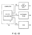
- Fig. 13 is a block diagram showing that the power source circuit in accordance with the above embodiment of the present invention is provided at a personal computer.
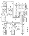
- Fig. 1 is a block diagram for explaining a power source system in accordance with one embodiment of the present invention.
- This power source system is used in a personal computer, for instance, and comprises a power source circuit and a power source controller.
- the power source circuit has, as shown in Fig. 1, AC adapter 1, battery 2, and DC/DC converter 3.
- AC adapter 1 is connected with a commercially available alternating current source, and puts out through output terminal 1a a direct current having a voltage of, for instance, +18V.
- Output terminal 1a is connected with voltage detector 5.
- Voltage detector 5 detects a voltage of output terminal 1a, and puts out detected result A1 (a voltage level value).
- Battery 2 is connected with output terminal 1b of AC adapter 1, and is charged by a charging output power from AC adapter 1.
- Battery 2 puts out through output terminal 2a a direct current having a voltage of, for instance, +18V.
- Output terminal 2a is connected with voltage detector 6.
- Voltage detector 6 detects a voltage of output terminal 2a (including charged voltage), and puts out detected result A2 (a voltage level value).
- Current detector 7 is connected with output terminal 2b of battery 2. It detects the charged current of battery 2, and puts out detected result A3 (a current level value).
- DC/DC converter 3 receives a direct current voltage supplied from output terminal 1a of AC adapter 1 through reverse current preventing diode 8, or a direct current voltage supplied from output terminal 2a of battery 2 through reverse current preventing diode 9.
- DC/DC converter 3 converts the input voltage from AC adapter 1 or battery 2 into various direct current voltages, for instance, +5V output voltage V1, -9V output voltage V2, and +12V output voltage V3, and they are respectively put out through output terminals 3a, 3b, and 3c.
- the power source circuit including DC/DC converter 3 is provided within personal computer 30 as shown in Fig. 13.
- Computer 30 is connected with various peripheral units such as CRT display unit 31, extended RAM 32, and hard disk drive unit (HDD) 33.
- DC/DC converter 3 supplies output voltage V1 from output terminal 3a to extended RAM 32, output voltage V2 from output voltage 3b to CRT display unit 31, and output voltage V3 from output terminal 3c to HDD 33.
- Voltage detector 10 is connected with output terminal 3a of DC/DC converter 3, detects output voltage V1, and puts out detected result A4 (a voltage level value).
- DC/DC converter 3 has output terminals 3b and 3c which are respectively connected with short-circuit detectors 11 and 12.
- Short-circuit detector 11 connected with output terminal 3b comprises resistance circuit 11a, diode 11b, and inverter 11c.
- Short-circuit detector 12 connected with output terminal 3c comprises resistance circuit 12a and diode 12b. Short-circuit detector 12 puts out detection signal D2 having a low level when a short-circuit has produced at output terminal 3c. In contrast, when output terminal 3c is in a normal condition, output signal D2 put out of short-circuit detector 12 is in a high level.
- Temperature sensor 13 is provided near the power source circuit comprising AC adapter 1, battery 2, and DC/DC converter 3. Temperature sensor 13 detects an ambient temperature and puts out detection result A5 (a voltage level value corresponding to the temperature value).
- Power source controller 4 performs an operation of detecting an occurrence of a power failure in the power source circuit having the above structure.
- Power source controller 4 has micro-processor (CPU) 20, random access memory (RAM) 21, read only memory (ROM) 22, timer 23, a first input port 24, and a second input port 25.
- CPU micro-processor
- RAM random access memory
- ROM read only memory
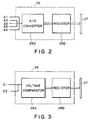
- First input port 24 receives detection signals D1 and D2 respectively supplied from short-circuit detectors 11 and 12, converts them into short-circuit detection data, and puts out the data to internal bus 27.
- First input port 24 has as shown in Fig. 3 voltage comparator 24a and register 24b.
- Voltage comparator 24a converts supplied detection signal D1 or supplied detection signal D2 into short-circuit detection data and puts out the converted data into register 24b.
- Register 24b holds the short-circuit detection data and puts them out to internal bus 27.
- Second input port 25 receives detection signals A1 through A5 respectively supplied from voltage detectors 5, 6 and 10, current detector 7, and temperature sensor 13, and performs an analog/digital conversion process.
- Second input port 25 has analog/digital converter (A/D converter) 25a and register 25b, as shown in Fig. 2.
- A/D converter 25a converts detection signals A1 through A5, which are each supplied as an analog signal, into digital signals, and puts out the digital signals into register 25b.
- Register 25b holds the digital signals and puts then out to internal bus 27.
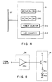
- RAM 21 stores data which are necessary for CPU 20 to perform a failure detection process.
- RAM 21 has error status register 21a, copying register 21b, timer counter register 21c, and LED counter register 21d, as shown in Fig. 4.
- Error status register 21a stores error status data (four-bit data b3 - b0) which are obtained by the failure detecting process performed by CPU 20 and indicate a kind to which the error condition (failure condition) of the power source circuit belongs.
- Copy register 21b stores a copy of the error status data stored in error status register 21a.
- Timer counter register 21c holds a timer count value obtained by CPU 20 counting clock pulses generated from timer 23.
- LED counter register 21d stores count values (CV) which are necessary for putting on or off the blinker device 14 comprising light emitting diodes (LEDs).
- ROM 22 stores a program necessary for CPU 20 to perform the failure detection process, and a table comprising error condition kind data and error status data.
- Blinker device 14 blinks in an orderly fashion that fits for the kind of error condition of the power source circuit which is obtained by a process of detecting the failure condition of the power source controller 4.
- Blinker device 14 comprises a circuit having LED 14a, transistor 14b, and resistor 14c, as shown in Fig. 5.
- Blinker device 14 operates as follows: When power source voltage V is applied to LED 14a due to the operation of transistor 14b, LED 14a emits light, whereas LED 14a stops emitting light when the application of the power source voltage V is shut off due to the operation of transistor 14b.
- Transistor 14b in blinker device 14 is driven by a driving signal put out of output port 26 of power source controller 4.
- Output port 26 has driver 26a, as shown in Fig. 5.
- Output port 26 is controlled by CPU 20 through internal bus 27 and puts out its driving signal through driver 26a.
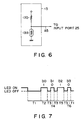
- Temperature sensor 13 comprises, as shown in Fig. 6, thermistor 13a and resistor 13b, and supplies detection signal (a voltage level value) A5 corresponding to the ambient temperature to second input port 25.
- Power source controller 4 performs the failure detection process based on detection signals A1 through A5 and detection signals D1 and D2, all detection signals being supplied from the power source circuit, and generates error status data (data b3 - b0) indicating the kind of failure condition of the power source circuit.
- the generated error status data are temporarily stored in error status register 21a.
- a variety of error status data are previously prepared in accordance with various kinds of failure conditions, and are stored in ROM 22 as a table.
- CPU 20 in power source controller 4 detects that the power source circuit is in a failure condition based on detection signals A1 through A5 and detection signals D1 and D2, it looks up from the table of ROM 22 error status data which correspond to the kind of the error condition of the circuit. Then, CPU 20 stores the looked up error status data into error status register 21a.
- Error status data "0101" indicates that battery 2 is in a charge failure condition (a voltage failure).
- Data "0001” indicates that AC adapter 1 is in an output voltage failure condition.
- Data "0010” indicates that the power source circuit is in a temperature failure condition.
- Data "1000” indicates that battery 2 is in a charge failure condition (current failure).
- Data "0111” indicates that output terminal 3a of DC/DC converter 3 is in an output voltage failure condition.
- Data "1001" (detection signal D1) indicates that output terminal 3b of DC/DC converter 3 is short-circuited.
- Data "1010” indicates that output terminal 3c of DC/DC converter 3 is short-circuited. In this way, the total of fifteen kinds of error conditions can be indicated by four-bit error status data.
- Voltage detector 6 is connected with output terminal 2a of battery 2, as shown in Fig. 1, and detects a voltage value of output terminal 2a.
- the voltage value of output terminal 2a indicates both an output voltage value of battery 2 and a charging voltage value from AC adapter 1.
- Voltage detector 6 puts out to second input port 25 of power source controller 4 detection signal A2 which corresponds to the detection results or the voltage level value.
- Second input port 25 converts inputted detection signal A2 into a digital signal and stores it in register 25b (see Fig. 2).
- CPU 20 receives from register 25b data corresponding to detection signal A2 and executes a power failure detection process.
- CPU 20 executes a program for the power failure detection process previously stored in ROM 22, and compares a previously set normal voltage level value with the voltage level value detected by voltage detector 6.
- CPU 20 judges that a charge failure condition occurs at battery 2, and sets, to error status register 21a, error status data "0101" indicating that battery 2 is in a charge failure condition (voltage failure).
- CPU 20 executes a blinker control process in which blinker 14 is driven for notifying the charge failure condition (voltage failure).
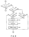
- the blinker control process has such contents as shown in a flow chart of Fig. 8 through Fig. 12.
- CPU 20 resets LED counter register 21d and the count value (CV) is set to an initial value "0" (Step S2). After having set error status data "0101" to error status register 21a in accordance with the power failure detection process (YES in Step S1), CPU 20 judges whether count value CV of counter register 21d is "0" or not (Step S3). Since YES in this case, CPU 20 drives timer 23 (Step S4), and increments count value CV of counter register 21d to set it to "1" (Step S5).
- Timer 23 generates a clock pulse having a predetermined cycle (65 ms, for instance).
- CPU 20 counts the clock pulse from timer 23, and sets timer count value T to timer counter register 21. Therefore, timer count value T which is renewed each time a predetermined time has passed from a start of timer 23 is set to timer counter register 21.
- CPU 20 controls driver 26a to turn off transistor 14b for the purpose of putting off LED 14a, as shown in Fig. 5 (Step S6). Namely, as shown in Fig. 7, a blinking operation begins in which LED turns off for a time T1 at an initial state. Time T1 is 2 seconds, for instance.
- CPU 20 repeats a loop consisting of YES in Step S1, NO in Step S3, YES in Step S7, and NO in Step S8.
- Step S8 After a condition that LED 14a is extinguished has passed for time T1 (YES in Step S8), CPU 20 drives timer 23 again (Step S9), and increments count value CV of counter register 21d to set it to "2" (Step S10). Therefore, timer count value T of timer counter register 21 begins at "0".
- CPU 20 controls driver 26a to turn on transistor 14b for the purpose of putting on LED 14a (Step S11). Since count value CV of counter register 21d is set to "2", CPU 20 moves to a process for judging first bit b0 of an error status data (Step S13). In this process, CPU 20 sets error status data "0101" to error status register 21a, and copies the set data to copy register 21b. CPU 20 shifts through copy register 21b, and judges bit by bit the entire data from first bit b0.
- Step S13 Since it is judged from a judging operation of Step S13 that first bit b0 of the error status data is "1", CPU 20 controls to light up LED 14a for one second (Steps S11 through S14). Namely, as shown in Fig. 7, LED 14a is controlled to light up for time T2 which corresponds to one second.
- CPU 20 increments count value CV of counter register 21d to set it to "3" (Step S16).
- CPU 20 further controls to extinguish LED 14a (Step S17), and drives timer 23 again (Step S18).
- CPU 20 judges whether count value CV of counter register 21d is "3" or not (Step S19). Since it is YES in this case, CPU 20 controls to keep the extinct condition of LED 14a for 0.5 seconds (Step S20). Namely, as shown in Fig. 7, the extinct condition of LED 14a continues for time T3.
- CPU 20 drives timer 23 again (Step S21), and increments count value CV of counter register 21d to set it to "4" (Step S22).
- CPU 20 furthermore controls to light up LED 14a (Step S23).
- Step S25 Since count value CV of counter register 21d is set to "4", CPU 20 moves to a process for judging second bit b1 of the error status data (Step S25). Since it is found that second bit b1 of the error status data is "0", CPU 20 controls to light up LED 14a for 0.5 seconds (Step S23 through Step S27). Namely, as shown in Fig. 7, LED 14 is controlled to light up for time T4 corresponding to 0.5 seconds.
- Step S27 When timer count value T reaches 0.5 seconds (YES in Step S27), CPU 20 increments count value CV of counter register 21d to set it to "5" (Step S28). Furthermore, CPU 20 controls to extinguish LED 14a, and drives timer 23 again (Step 30).
- CPU 20 judges whether count value CV of counter register 21d is "5" or not (Step S31). Since it is YES in this case, CPU 20 controls to continue the extinct condition of LED 14a for 0.5 seconds (Step S32). Namely, as shown in Fig. 7, extinction of LED 14a continues for time T3.
- Step S32 After the extinction of LED 14a continues for time T3 (YES in Step S32), CPU 20 drives timer 23 again (Step S33), and increment count value CV of counter register 21d to set it to "6" (Step S34). Furthermore, CPU 20 controls to light up LED 14a (Step S35).
- Step S37 Since count value CV of counter register 21d is set to "6", CPU 20 moves to a process for judging third bit b2 of the error status data (Step S37). Since it is found out from the judgment process that third bit b2 of the error status data is "1", CPU 20 controls to light up LED 14a for one second (Step S35 through Step S38). Namely, as shown in Fig. 7, LED 14a is controlled to light up for time T5 corresponding to one second.
- Step S38 CPU 20 increments count value CV of counter register 21d to set it to "7" (Step S40). Furthermore, CPU 20 controls to extinguish LED 14a (Step S41), and drives timer 23 again (Step S42).
- CPU 20 judges whether count value CV of counter register 21d is "7" or not (Step S43). Since it is YES in this case, CPU 20 controls to continue the extinguished condition of LED 14a for 0.5 seconds (Step S44). Namely, as shown in Fig. 7, the condition that LED 14a is extinct continues for time T3.
- Step S44 After the extinction of LED 14a has passed for time T3 (YES in Step S44), CPU 20 drives timer 23 again (Step S45), and increments count value CV of counter register 21d to set it to "8" (Step S46). Furthermore, CPU 20 controls to light up LED 14a (Step S47).
- Step S49 Since count value CV of counter register 21d is set to "8", CPU 20 moves to a process for judging fourth bit b3 of the error status data (Step S49). Since it is found out from this judgment process that fourth bit b3 of the error status data is "0", CPU 20 controls to light up LED 14a for 0.5 seconds (Step S47 through Step S49, and Step S51). Namely, as shown in Fig. 7, LED 14a is controlled to light up for time T6 which corresponds to 0.5 seconds.
- Step S51 After timer count value T has reached 0.5 seconds (YES in Step S51), CPU 20 increments count value CV of counter register 21d to set it to "9" (Step S52). Furthermore, CPU 20 controls to extinguish LED 14a (Step S53), and drives timer 23 again (Step S54).
- CPU 20 judges whether count value CV of counter register 21d is "8" or not (Step S48). Since it is NO in this case, CPU 20 judges whether count value CV is bigger than "8" or not (Step S55). Since count value CV is "9" (YES in Step S55), CPU 20 sets count value CV to an initial value "0" (Step S56).
- power source controller 4 detects that battery 2 of the power source circuit is in a power failure condition (power failure), and sets to register 21a an error status data "0101" which corresponds to a kind of power failure condition. Based on the error status data "0101", the power source controller controls to light up and extinguish blinker 14 (LED 14a) for the purpose of notifying a charge failure condition.
- LED 14a blinker 14
- LED is on-off controlled corresponding to a value of each bit in the error status data "0101".
- a charge failure condition the condition that the LED is lit up for one second and then is extinguished for 0.5 seconds is repeated.
- the user sees the blinking condition of blinker 14, and understands that a charge failure condition (voltage failure) occurs at battery 2 of the power source circuit.
- the error status data in the above embodiment has four bits, but it is possible that the error status data has more than four bits. The number of bits in the error status data determines the number of kinds of failure conditions which the device can notify.
Description
- The present invention relates to a power controlling apparatus for detecting a power failure of a power source circuit, which is used in an electronic equipment such as a personal computer, and displaying detected results.
- Hitherto an electronic equipment such as a personal computer uses as its power source a commercially available alternating current source (an AC source) or a chargeable battery (a chargeable internal battery). It uses a DC/DC converter, etc., to generate various direct currents, each having its own necessary voltage level (a DC voltage), from the power source circuit which uses either one of the above-mentioned power sources and to provide the currents thus obtained to the various circuits in the electronic equipment.
- The electronic equipment has a device which detects an occurrence of a power failure at the power source circuit and notifies an operator of the power failure. Such a device monitors an output voltage level of the power source circuit and causes a warning device having a light emitting diode, etc., to light up when the detected voltage level is outside an allowable range.
- The above electronic equipment may surely notify the operator of the occurrence of a power failure in the power source circuit by lighting up the display device, but it cannot notify the operator of a particular part of the power source circuit which is in failure or details of the failure. For instance, it is impossible for the operator to determine from the information of the warning device whether the failure in question occurs in the AC power source circuit or the battery. Furthermore, if the failure in the power source circuit occurs due to the variation in temperature around the electronic equipment, the operator cannot find the cause of the failure.
- Accordingly, upon repair of the power source circuit, the whole of the power source circuit must be examined thoroughly to find out a failure part or a failure cause. This means that a laborious complicated checking work must be done to repair the power source circuit and to restore the electronic equipment to the original normal condition.
- Prior art document US-A-4 600 962 discloses a power controlling apparatus with a power failure detecting function. In this apparatus, failure data processing means identify power failure conditions, e.g. overvoltage, undervoltage, high temperature, humidity and generate failure status data.
- It is an object of the present invention to realize a power controlling apparatus which surely detects an occurrence of a power failure in a power source circuit used in an electronic equipment such as a personal computer and notifies an operator of details of the detected power source failure, such as a failed portion or a failure cause.
- To solve this object the present invention provides a power controlling apparatus as specified in
claim 1. - Upon detection of the power source circuit being in a failure condition, the apparatus in the present invention visually notifies an operator of the kind of the failure, such as a failure portion or a failure cause, by blinking in an orderly fashion which fits to power failure conditions of the detected kind.
- This invention can be more fully understood from the following detailed description when taken in conjunction with the accompanying drawings, in which:
- Fig. 1 is a block diagram showing a structure of a power source system in accordance with one embodiment of the present invention.
- Fig. 2 is a block diagram showing a structure of an input port of a power source controller in accordance with the above embodiment of the present invention.
- Fig. 3 is a block diagram showing a structure of another input port of the power source controller in accordance with the above embodiment of the present invention.
- Fig. 4 is a block diagram showing a structure of a RAM in the power source controller in accordance with the above embodiment of the present invention.
- Fig. 5 is a block diagram showing a structure of an output port and a blinker device in accordance with the above embodiment of the present invention.
- Fig. 6 is a circuit diagram showing a structure of a temperature sensor in accordance with the above embodiment of the present invention.
- Fig. 7 is a timing chart for explaining operation of the above embodiment of the present invention.
- Fig. 8 through Fig. 12 are a flow chart for explaining operation of the above embodiment of the present invention.
- Fig. 13 is a block diagram showing that the power source circuit in accordance with the above embodiment of the present invention is provided at a personal computer.
- Now, one embodiment of the present invention will be explained below with reference to the drawings.
- Fig. 1 is a block diagram for explaining a power source system in accordance with one embodiment of the present invention. This power source system is used in a personal computer, for instance, and comprises a power source circuit and a power source controller.
- The power source circuit has, as shown in Fig. 1,
AC adapter 1,battery 2, and DC/DC converter 3.AC adapter 1 is connected with a commercially available alternating current source, and puts out through output terminal 1a a direct current having a voltage of, for instance, +18V. Output terminal 1a is connected withvoltage detector 5.Voltage detector 5 detects a voltage of output terminal 1a, and puts out detected result A1 (a voltage level value). -
Battery 2 is connected with output terminal 1b ofAC adapter 1, and is charged by a charging output power fromAC adapter 1.Battery 2 puts out through output terminal 2a a direct current having a voltage of, for instance, +18V. Output terminal 2a is connected withvoltage detector 6.Voltage detector 6 detects a voltage of output terminal 2a (including charged voltage), and puts out detected result A2 (a voltage level value).Current detector 7 is connected withoutput terminal 2b ofbattery 2. It detects the charged current ofbattery 2, and puts out detected result A3 (a current level value). - DC/
DC converter 3 receives a direct current voltage supplied from output terminal 1a ofAC adapter 1 through reversecurrent preventing diode 8, or a direct current voltage supplied from output terminal 2a ofbattery 2 through reversecurrent preventing diode 9. DC/DC converter 3 converts the input voltage fromAC adapter 1 orbattery 2 into various direct current voltages, for instance, +5V output voltage V1, -9V output voltage V2, and +12V output voltage V3, and they are respectively put out throughoutput terminals - The power source circuit including DC/
DC converter 3 is provided withinpersonal computer 30 as shown in Fig. 13.Computer 30 is connected with various peripheral units such asCRT display unit 31,extended RAM 32, and hard disk drive unit (HDD) 33. DC/DC converter 3 supplies output voltage V1 fromoutput terminal 3a toextended RAM 32, output voltage V2 fromoutput voltage 3b toCRT display unit 31, and output voltage V3 from output terminal 3c toHDD 33. -
Voltage detector 10 is connected withoutput terminal 3a of DC/DC converter 3, detects output voltage V1, and puts out detected result A4 (a voltage level value). - DC/
DC converter 3 hasoutput terminals 3b and 3c which are respectively connected with short-circuit detectors 11 and 12. Short-circuit detector 11 connected withoutput terminal 3b comprises resistance circuit 11a, diode 11b, and inverter 11c. When short-circuit detector 11 detects that a short-circuit is produced atoutput terminal 3b, it puts out detection signal D1 having a low level. In contrast, whenoutput terminal 3b is in a normal condition, output signal D1 put out of short-circuit detector 11 is in a high level. Short-circuit detector 12 connected with output terminal 3c comprises resistance circuit 12a and diode 12b. Short-circuit detector 12 puts out detection signal D2 having a low level when a short-circuit has produced at output terminal 3c. In contrast, when output terminal 3c is in a normal condition, output signal D2 put out of short-circuit detector 12 is in a high level. -
Temperature sensor 13 is provided near the power source circuit comprisingAC adapter 1,battery 2, and DC/DC converter 3.Temperature sensor 13 detects an ambient temperature and puts out detection result A5 (a voltage level value corresponding to the temperature value). -
Power source controller 4 performs an operation of detecting an occurrence of a power failure in the power source circuit having the above structure.Power source controller 4 has micro-processor (CPU) 20, random access memory (RAM) 21, read only memory (ROM) 22,timer 23, afirst input port 24, and asecond input port 25. -
First input port 24 receives detection signals D1 and D2 respectively supplied from short-circuit detectors 11 and 12, converts them into short-circuit detection data, and puts out the data tointernal bus 27.First input port 24 has as shown in Fig. 3voltage comparator 24a and register 24b.Voltage comparator 24a converts supplied detection signal D1 or supplied detection signal D2 into short-circuit detection data and puts out the converted data intoregister 24b. Register 24b holds the short-circuit detection data and puts them out tointernal bus 27. -
Second input port 25 receives detection signals A1 through A5 respectively supplied fromvoltage detectors current detector 7, andtemperature sensor 13, and performs an analog/digital conversion process.Second input port 25 has analog/digital converter (A/D converter) 25a and register 25b, as shown in Fig. 2. A/D converter 25a converts detection signals A1 through A5, which are each supplied as an analog signal, into digital signals, and puts out the digital signals intoregister 25b. Register 25b holds the digital signals and puts then out tointernal bus 27. -
RAM 21 stores data which are necessary forCPU 20 to perform a failure detection process.RAM 21 has error status register 21a, copyingregister 21b, timer counter register 21c, and LED counter register 21d, as shown in Fig. 4. - Error status register 21a stores error status data (four-bit data b3 - b0) which are obtained by the failure detecting process performed by
CPU 20 and indicate a kind to which the error condition (failure condition) of the power source circuit belongs.Copy register 21b stores a copy of the error status data stored in error status register 21a. Timer counter register 21c holds a timer count value obtained byCPU 20 counting clock pulses generated fromtimer 23. LED counter register 21d stores count values (CV) which are necessary for putting on or off theblinker device 14 comprising light emitting diodes (LEDs). -
ROM 22 stores a program necessary forCPU 20 to perform the failure detection process, and a table comprising error condition kind data and error status data. -
Blinker device 14 blinks in an orderly fashion that fits for the kind of error condition of the power source circuit which is obtained by a process of detecting the failure condition of thepower source controller 4.Blinker device 14 comprises acircuit having LED 14a,transistor 14b, and resistor 14c, as shown in Fig. 5.Blinker device 14 operates as follows: When power source voltage V is applied toLED 14a due to the operation oftransistor 14b,LED 14a emits light, whereasLED 14a stops emitting light when the application of the power source voltage V is shut off due to the operation oftransistor 14b. -
Transistor 14b inblinker device 14 is driven by a driving signal put out ofoutput port 26 ofpower source controller 4.Output port 26 hasdriver 26a, as shown in Fig. 5.Output port 26 is controlled byCPU 20 throughinternal bus 27 and puts out its driving signal throughdriver 26a. -
Temperature sensor 13 comprises, as shown in Fig. 6,thermistor 13a andresistor 13b, and supplies detection signal (a voltage level value) A5 corresponding to the ambient temperature tosecond input port 25. - Now, the operation of the above-mentioned embodiment will be explained below.
-
Power source controller 4 performs the failure detection process based on detection signals A1 through A5 and detection signals D1 and D2, all detection signals being supplied from the power source circuit, and generates error status data (data b3 - b0) indicating the kind of failure condition of the power source circuit. The generated error status data are temporarily stored in error status register 21a. - A variety of error status data are previously prepared in accordance with various kinds of failure conditions, and are stored in
ROM 22 as a table. WhenCPU 20 inpower source controller 4 detects that the power source circuit is in a failure condition based on detection signals A1 through A5 and detection signals D1 and D2, it looks up from the table ofROM 22 error status data which correspond to the kind of the error condition of the circuit. Then,CPU 20 stores the looked up error status data into error status register 21a. - Some examples of the correspondence relationship between error status data and kinds of error conditions will be shown below.
- Error status data "0101" (detection signal A2) indicates that
battery 2 is in a charge failure condition (a voltage failure). Data "0001" (detection signal A1) indicates thatAC adapter 1 is in an output voltage failure condition. Data "0010" (detection signal A5) indicates that the power source circuit is in a temperature failure condition. Data "1000" (detection signal A3) indicates thatbattery 2 is in a charge failure condition (current failure). Data "0111" (detection signal A4) indicates thatoutput terminal 3a of DC/DC converter 3 is in an output voltage failure condition. Data "1001" (detection signal D1) indicates thatoutput terminal 3b of DC/DC converter 3 is short-circuited. Data "1010" (detection signal D2) indicates that output terminal 3c of DC/DC converter 3 is short-circuited. In this way, the total of fifteen kinds of error conditions can be indicated by four-bit error status data. - In the following explanation, a case that
battery 2 is in a charge failure condition (a voltage failure condition) will be explained. -
Voltage detector 6 is connected with output terminal 2a ofbattery 2, as shown in Fig. 1, and detects a voltage value of output terminal 2a. The voltage value of output terminal 2a indicates both an output voltage value ofbattery 2 and a charging voltage value fromAC adapter 1. -
Voltage detector 6 puts out tosecond input port 25 ofpower source controller 4 detection signal A2 which corresponds to the detection results or the voltage level value.Second input port 25 converts inputted detection signal A2 into a digital signal and stores it inregister 25b (see Fig. 2). -
CPU 20 receives fromregister 25b data corresponding to detection signal A2 and executes a power failure detection process. In detail,CPU 20 executes a program for the power failure detection process previously stored inROM 22, and compares a previously set normal voltage level value with the voltage level value detected byvoltage detector 6. - If the comparison result indicates that the detected voltage level value is outside of a permitted range,
CPU 20 judges that a charge failure condition occurs atbattery 2, and sets, to error status register 21a, error status data "0101" indicating thatbattery 2 is in a charge failure condition (voltage failure). -
CPU 20 executes a blinker control process in whichblinker 14 is driven for notifying the charge failure condition (voltage failure). The blinker control process has such contents as shown in a flow chart of Fig. 8 through Fig. 12. - As shown in Fig. 8,
CPU 20 resets LED counter register 21d and the count value (CV) is set to an initial value "0" (Step S2). After having set error status data "0101" to error status register 21a in accordance with the power failure detection process (YES in Step S1),CPU 20 judges whether count value CV of counter register 21d is "0" or not (Step S3). Since YES in this case,CPU 20 drives timer 23 (Step S4), and increments count value CV of counter register 21d to set it to "1" (Step S5).Timer 23 generates a clock pulse having a predetermined cycle (65 ms, for instance).CPU 20 counts the clock pulse fromtimer 23, and sets timer count value T totimer counter register 21. Therefore, timer count value T which is renewed each time a predetermined time has passed from a start oftimer 23 is set totimer counter register 21. -
CPU 20controls driver 26a to turn offtransistor 14b for the purpose of putting offLED 14a, as shown in Fig. 5 (Step S6). Namely, as shown in Fig. 7, a blinking operation begins in which LED turns off for a time T1 at an initial state. Time T1 is 2 seconds, for instance.CPU 20 repeats a loop consisting of YES in Step S1, NO in Step S3, YES in Step S7, and NO in Step S8. - After a condition that
LED 14a is extinguished has passed for time T1 (YES in Step S8),CPU 20drives timer 23 again (Step S9), and increments count value CV of counter register 21d to set it to "2" (Step S10). Therefore, timer count value T oftimer counter register 21 begins at "0". -
CPU 20controls driver 26a to turn ontransistor 14b for the purpose of putting onLED 14a (Step S11). Since count value CV of counter register 21d is set to "2",CPU 20 moves to a process for judging first bit b0 of an error status data (Step S13). In this process,CPU 20 sets error status data "0101" to error status register 21a, and copies the set data to copyregister 21b.CPU 20 shifts throughcopy register 21b, and judges bit by bit the entire data from first bit b0. - Since it is judged from a judging operation of Step S13 that first bit b0 of the error status data is "1",
CPU 20 controls to light upLED 14a for one second (Steps S11 through S14). Namely, as shown in Fig. 7,LED 14a is controlled to light up for time T2 which corresponds to one second. - When timer count value T becomes to indicate that one second has passed (YES in Step S14),
CPU 20 increments count value CV of counter register 21d to set it to "3" (Step S16).CPU 20 further controls to extinguishLED 14a (Step S17), and drivestimer 23 again (Step S18). -
CPU 20 judges whether count value CV of counter register 21d is "3" or not (Step S19). Since it is YES in this case,CPU 20 controls to keep the extinct condition ofLED 14a for 0.5 seconds (Step S20). Namely, as shown in Fig. 7, the extinct condition ofLED 14a continues for time T3. - After the condition that
LED 14a is extinguished continues for time T3 (YES in Step S20),CPU 20drives timer 23 again (Step S21), and increments count value CV of counter register 21d to set it to "4" (Step S22).CPU 20 furthermore controls to light upLED 14a (Step S23). - Since count value CV of counter register 21d is set to "4",
CPU 20 moves to a process for judging second bit b1 of the error status data (Step S25). Since it is found that second bit b1 of the error status data is "0",CPU 20 controls to light upLED 14a for 0.5 seconds (Step S23 through Step S27). Namely, as shown in Fig. 7,LED 14 is controlled to light up for time T4 corresponding to 0.5 seconds. - When timer count value T reaches 0.5 seconds (YES in Step S27),
CPU 20 increments count value CV of counter register 21d to set it to "5" (Step S28). Furthermore,CPU 20 controls to extinguishLED 14a, and drivestimer 23 again (Step 30). -
CPU 20 judges whether count value CV of counter register 21d is "5" or not (Step S31). Since it is YES in this case,CPU 20 controls to continue the extinct condition ofLED 14a for 0.5 seconds (Step S32). Namely, as shown in Fig. 7, extinction ofLED 14a continues for time T3. - After the extinction of
LED 14a continues for time T3 (YES in Step S32),CPU 20drives timer 23 again (Step S33), and increment count value CV of counter register 21d to set it to "6" (Step S34). Furthermore,CPU 20 controls to light upLED 14a (Step S35). - Since count value CV of counter register 21d is set to "6",
CPU 20 moves to a process for judging third bit b2 of the error status data (Step S37). Since it is found out from the judgment process that third bit b2 of the error status data is "1",CPU 20 controls to light upLED 14a for one second (Step S35 through Step S38). Namely, as shown in Fig. 7,LED 14a is controlled to light up for time T5 corresponding to one second. - After timer count value T becomes one second (YES in Step S38),
CPU 20 increments count value CV of counter register 21d to set it to "7" (Step S40). Furthermore,CPU 20 controls to extinguishLED 14a (Step S41), and drivestimer 23 again (Step S42). -
CPU 20 judges whether count value CV of counter register 21d is "7" or not (Step S43). Since it is YES in this case,CPU 20 controls to continue the extinguished condition ofLED 14a for 0.5 seconds (Step S44). Namely, as shown in Fig. 7, the condition thatLED 14a is extinct continues for time T3. - After the extinction of
LED 14a has passed for time T3 (YES in Step S44),CPU 20drives timer 23 again (Step S45), and increments count value CV of counter register 21d to set it to "8" (Step S46). Furthermore,CPU 20 controls to light upLED 14a (Step S47). - Since count value CV of counter register 21d is set to "8",
CPU 20 moves to a process for judging fourth bit b3 of the error status data (Step S49). Since it is found out from this judgment process that fourth bit b3 of the error status data is "0",CPU 20 controls to light upLED 14a for 0.5 seconds (Step S47 through Step S49, and Step S51). Namely, as shown in Fig. 7,LED 14a is controlled to light up for time T6 which corresponds to 0.5 seconds. - After timer count value T has reached 0.5 seconds (YES in Step S51),
CPU 20 increments count value CV of counter register 21d to set it to "9" (Step S52). Furthermore,CPU 20 controls to extinguishLED 14a (Step S53), and drivestimer 23 again (Step S54). -
CPU 20 judges whether count value CV of counter register 21d is "8" or not (Step S48). Since it is NO in this case,CPU 20 judges whether count value CV is bigger than "8" or not (Step S55). Since count value CV is "9" (YES in Step S55),CPU 20 sets count value CV to an initial value "0" (Step S56). - In this way,
power source controller 4 detects thatbattery 2 of the power source circuit is in a power failure condition (power failure), and sets to register 21a an error status data "0101" which corresponds to a kind of power failure condition. Based on the error status data "0101", the power source controller controls to light up and extinguish blinker 14 (LED 14a) for the purpose of notifying a charge failure condition. - Namely, as shown in Fig. 7, LED is on-off controlled corresponding to a value of each bit in the error status data "0101". In case of a charge failure condition, the condition that the LED is lit up for one second and then is extinguished for 0.5 seconds is repeated. The user sees the blinking condition of
blinker 14, and understands that a charge failure condition (voltage failure) occurs atbattery 2 of the power source circuit. - In the above embodiment, "1" in each bit of the four bits stands for lighting up or extinguishing the LED for one second and "0" in each bit stands for lighting up or extinguishing the LED for 0.5 seconds. However, it is not restricted to this example. For instance, it is possible to light up or extinguish the LED for one second when each bit is "0", and to light up or extinguish the LED for 0.5 seconds when each bit is "1". In addition, the error status data in the above embodiment has four bits, but it is possible that the error status data has more than four bits. The number of bits in the error status data determines the number of kinds of failure conditions which the device can notify.
Claims (6)
- A power controlling apparatus with a power failure detecting function comprising- detecting means (5-7, 10-13) for detecting a power failure condition of a power source circuit and generating a failure detection signal;- failure data processing means (20-21) for identifying the power failure condition of the power source circuit based on the failure detection signal supplied from the detecting means, and generating failure status data in correspondence with a kind to which the identified power failure condition belongs; and- blinker means (14, 20,- 26) for blinking in a variety of fashions in correspondence with various kinds of power failure conditions based on the failure status data generated by the failure data processing means,characterized in that- said failure data processing means (20-21) includes a register (21a) having previously prepared number of a plurality of bit positions, and setting bit data at each of said bit positions of the register in accordance with the kind of the failure conditions; and- said blinker means (14, 20, 26) includes a light emitting diode (14a), and driving means for lighting up and extinguishing the light emitting diode (14a) at intervals to sequentially indicate the bit data of each of the bit positions, thereby to indicate the kind of the failure conditions set at the register (21a), wherein each bit data corresponds to a predetermined different on/off duration of the blinker means (14, 20, 26).
- The apparatus according to claim 1, characterized in that said detecting means (5-7, 10-13) has a voltage level detecting circuit for detecting a voltage level of an output from the power source circuit.
- The apparatus according to claim 1, characterized in that said detecting means (5-7, 10-13) has a temperature sensor (13) which detects an ambient temperature of the power source circuit and generates a voltage signal corresponding to the detected ambient temperature.
- The apparatus according to claim 1, characterized in that said detecting means (6) has a voltage level detecting circuit for detecting a level of a charged voltage of the power source circuit.
- The apparatus according to claim 1, characterized by further comprising blinker control means (20) having a timer counter (21c) for setting on/off duration for the blinker means (14, 20, 26), for lighting up the blinker means (14, 20, 26) for every bit of the failure status data, and controlling to set a lighting duration of the blinker means (14, 20, 26) in accordance with each bit data based on the timer count value of the time counter (21c).
- The apparatus according to claim 1, characterized by further comprising blinker control means (20) having an LED counter (21d) for holding and LED count value based on a bit position number of the failure status data and a timer counter for setting on/off duration for the blinker means (14, 20, 26), and controlling to set a light duration of the blinker means (14, 20, 26) in accordance with each bit data based on the time count value of the timer counter.
Applications Claiming Priority (2)
| Application Number | Priority Date | Filing Date | Title |
|---|---|---|---|
| JP301690/90 | 1990-11-07 | ||
| JP2301690A JPH04172539A (en) | 1990-11-07 | 1990-11-07 | Power supply condition display unit |
Publications (3)
| Publication Number | Publication Date |
|---|---|
| EP0484759A2 EP0484759A2 (en) | 1992-05-13 |
| EP0484759A3 EP0484759A3 (en) | 1993-02-24 |
| EP0484759B1 true EP0484759B1 (en) | 1995-12-13 |
Family
ID=17899975
Family Applications (1)
| Application Number | Title | Priority Date | Filing Date |
|---|---|---|---|
| EP91118195A Expired - Lifetime EP0484759B1 (en) | 1990-11-07 | 1991-10-24 | A power controlling apparatus with a power failure detecting function |
Country Status (5)
| Country | Link |
|---|---|
| US (1) | US5332993A (en) |
| EP (1) | EP0484759B1 (en) |
| JP (1) | JPH04172539A (en) |
| KR (1) | KR940006803B1 (en) |
| DE (1) | DE69115447T2 (en) |
Families Citing this family (17)
| Publication number | Priority date | Publication date | Assignee | Title |
|---|---|---|---|---|
| KR0157847B1 (en) * | 1993-04-07 | 1999-05-15 | 미따라이 하지메 | Information output apparatus and method utilizing multi-function mode indicator |
| US5905347A (en) * | 1993-07-16 | 1999-05-18 | Dell Usa, L.P. | System and method for controlling a computer drive motor |
| US5650771A (en) * | 1995-04-25 | 1997-07-22 | Lee; Chung-Cheng | Electrical socket with monitoring unit for monitoring operating conditions |
| US5946404A (en) * | 1995-06-01 | 1999-08-31 | Silent Witness Enterprises Ltd. | Audio/video surveillance and recording system |
| US5724026A (en) * | 1996-04-24 | 1998-03-03 | International Business Machines Corporation | Multiple output level power supply with overpower detection circuit |
| US6523124B1 (en) * | 1999-04-23 | 2003-02-18 | Palm, Inc. | System and method for detection of an accessory device connection status |
| JP2002142447A (en) * | 2000-10-31 | 2002-05-17 | Sony Corp | Power supply apparatus and electronic equipment |
| JP3830910B2 (en) | 2003-03-04 | 2006-10-11 | 株式会社東芝 | Fuel cell unit and status display control method |
| US7836216B2 (en) * | 2005-08-23 | 2010-11-16 | Palm, Inc. | Connector system for supporting multiple types of plug carrying accessory devices |
| KR20070069560A (en) * | 2005-12-28 | 2007-07-03 | 엘지전자 주식회사 | Apparatus and method of displaying hardware error in computer booting |
| US7642671B2 (en) * | 2006-04-28 | 2010-01-05 | Acco Brands Usa Llc | Power supply system providing two output voltages |
| US7734841B2 (en) * | 2006-06-30 | 2010-06-08 | Palm, Inc. | System and method for providing serial bus connectivity |
| FI20065783A0 (en) * | 2006-12-08 | 2006-12-08 | Nokia Corp | Signal pre-distortion in radio transmitters |
| CN101861025B (en) * | 2010-06-10 | 2014-07-09 | 鸿富锦精密工业(深圳)有限公司 | LED light emitting device and drive circuit thereof |
| JP6299191B2 (en) | 2013-12-05 | 2018-03-28 | 株式会社リコー | Electronic device abnormality display device |
| CN111491410A (en) * | 2020-04-30 | 2020-08-04 | 山东省计算中心(国家超级计算济南中心) | Method for indicating multiple states by one indicator light |
| EP4075434B1 (en) * | 2021-04-12 | 2023-11-08 | Samsung Electronics Co., Ltd. | Overvoltage detection in storage device and provision of status information |
Family Cites Families (5)
| Publication number | Priority date | Publication date | Assignee | Title |
|---|---|---|---|---|
| US3940679A (en) * | 1974-06-18 | 1976-02-24 | Textron, Inc. | Nickel-cadmium battery monitor |
| US4335413A (en) * | 1980-04-15 | 1982-06-15 | Westinghouse Electric Corp. | Circuit interrupter with remote indicator and power supply |
| US4307389A (en) * | 1980-04-25 | 1981-12-22 | Ford Motor Company | Decoding circuit |
| US4553081A (en) * | 1982-06-07 | 1985-11-12 | Norand Corporation | Portable battery powered system |
| US4600962A (en) * | 1983-02-03 | 1986-07-15 | Sentec Inc. | Apparatus for monitoring and protecting a device against a plurality of fault conditions |
-
1990
- 1990-11-07 JP JP2301690A patent/JPH04172539A/en active Pending
-
1991
- 1991-10-24 EP EP91118195A patent/EP0484759B1/en not_active Expired - Lifetime
- 1991-10-24 DE DE69115447T patent/DE69115447T2/en not_active Expired - Fee Related
- 1991-10-30 US US07/784,710 patent/US5332993A/en not_active Expired - Lifetime
- 1991-11-06 KR KR1019910019643A patent/KR940006803B1/en not_active IP Right Cessation
Also Published As
| Publication number | Publication date |
|---|---|
| DE69115447T2 (en) | 1996-05-02 |
| KR940006803B1 (en) | 1994-07-27 |
| DE69115447D1 (en) | 1996-01-25 |
| KR920010401A (en) | 1992-06-26 |
| US5332993A (en) | 1994-07-26 |
| EP0484759A2 (en) | 1992-05-13 |
| EP0484759A3 (en) | 1993-02-24 |
| JPH04172539A (en) | 1992-06-19 |
Similar Documents
| Publication | Publication Date | Title |
|---|---|---|
| EP0484759B1 (en) | A power controlling apparatus with a power failure detecting function | |
| US5270946A (en) | Method and apparatus for controlling selection of batteries | |
| JP2530717B2 (en) | Battery voltage determination circuit | |
| US6483274B2 (en) | Device and method for displaying charge capacity information of smart battery | |
| US4428020A (en) | Power supply sensing circuitry | |
| JP3234191B2 (en) | Electronic device and power supply monitoring method in the electronic device | |
| KR101649704B1 (en) | Power failure monitoring apparatus for digital protecting relay | |
| US4847720A (en) | Power supply output protection circuitry with signaling | |
| EP0335316A2 (en) | Apparatus for controlling selection of batteries | |
| US5644211A (en) | Malfunction prevention circuit for a battery charger | |
| US5027328A (en) | Memory drive device and method | |
| JPH0868986A (en) | Back light controller | |
| KR200259103Y1 (en) | Apparatus for changing Switch in Uninterruptible Power System | |
| JP2900124B2 (en) | Uninterruptible power system | |
| JPH10189213A (en) | Gas engine spark plug monitoring device | |
| JPS61247980A (en) | Power source voltage detector | |
| JP3164729B2 (en) | Power management mechanism for battery starter | |
| JP3438152B2 (en) | Automatic fire alarm | |
| KR970003351Y1 (en) | Driving error detection device of gto | |
| KR920000823B1 (en) | Power failure protection method and circuit for electronic cooking machine | |
| KR19990025726A (en) | Battery discharge state monitoring circuit | |
| JPS603563A (en) | Commercial power source frequency discriminating device | |
| JPH0799897B2 (en) | Disconnection or short circuit failure detection device | |
| JPH0338665A (en) | Image forming device | |
| JPH0662527A (en) | Electrical power supply apparatus using storage battery |
Legal Events
| Date | Code | Title | Description |
|---|---|---|---|
| PUAI | Public reference made under article 153(3) epc to a published international application that has entered the european phase |
Free format text: ORIGINAL CODE: 0009012 |
|
| 17P | Request for examination filed |
Effective date: 19911121 |
|
| AK | Designated contracting states |
Kind code of ref document: A2 Designated state(s): DE FR GB |
|
| PUAL | Search report despatched |
Free format text: ORIGINAL CODE: 0009013 |
|
| AK | Designated contracting states |
Kind code of ref document: A3 Designated state(s): DE FR GB |
|
| 17Q | First examination report despatched |
Effective date: 19940208 |
|
| GRAA | (expected) grant |
Free format text: ORIGINAL CODE: 0009210 |
|
| AK | Designated contracting states |
Kind code of ref document: B1 Designated state(s): DE FR GB |
|
| REF | Corresponds to: |
Ref document number: 69115447 Country of ref document: DE Date of ref document: 19960125 |
|
| ET | Fr: translation filed | ||
| PLBE | No opposition filed within time limit |
Free format text: ORIGINAL CODE: 0009261 |
|
| STAA | Information on the status of an ep patent application or granted ep patent |
Free format text: STATUS: NO OPPOSITION FILED WITHIN TIME LIMIT |
|
| 26N | No opposition filed | ||
| PGFP | Annual fee paid to national office [announced via postgrant information from national office to epo] |
Ref country code: GB Payment date: 19971015 Year of fee payment: 7 |
|
| PGFP | Annual fee paid to national office [announced via postgrant information from national office to epo] |
Ref country code: DE Payment date: 19971031 Year of fee payment: 7 |
|
| PGFP | Annual fee paid to national office [announced via postgrant information from national office to epo] |
Ref country code: FR Payment date: 19981009 Year of fee payment: 8 |
|
| PG25 | Lapsed in a contracting state [announced via postgrant information from national office to epo] |
Ref country code: GB Free format text: LAPSE BECAUSE OF NON-PAYMENT OF DUE FEES Effective date: 19981024 |
|
| GBPC | Gb: european patent ceased through non-payment of renewal fee |
Effective date: 19981024 |
|
| PG25 | Lapsed in a contracting state [announced via postgrant information from national office to epo] |
Ref country code: DE Free format text: LAPSE BECAUSE OF NON-PAYMENT OF DUE FEES Effective date: 19990803 |
|
| PG25 | Lapsed in a contracting state [announced via postgrant information from national office to epo] |
Ref country code: FR Free format text: LAPSE BECAUSE OF NON-PAYMENT OF DUE FEES Effective date: 20000630 |
|
| REG | Reference to a national code |
Ref country code: FR Ref legal event code: ST |