EP0484031A2 - Transkonduktanzverstärker mit drei Eingängen und verschmolzener Stromklemmschaltung, zur Verwendung in einem Oszillator - Google Patents
Transkonduktanzverstärker mit drei Eingängen und verschmolzener Stromklemmschaltung, zur Verwendung in einem Oszillator Download PDFInfo
- Publication number
- EP0484031A2 EP0484031A2 EP91309742A EP91309742A EP0484031A2 EP 0484031 A2 EP0484031 A2 EP 0484031A2 EP 91309742 A EP91309742 A EP 91309742A EP 91309742 A EP91309742 A EP 91309742A EP 0484031 A2 EP0484031 A2 EP 0484031A2
- Authority
- EP
- European Patent Office
- Prior art keywords
- input
- transconductor
- triple
- path
- source
- Prior art date
- Legal status (The legal status is an assumption and is not a legal conclusion. Google has not performed a legal analysis and makes no representation as to the accuracy of the status listed.)
- Granted
Links
- 230000010354 integration Effects 0.000 claims description 2
- 239000003990 capacitor Substances 0.000 description 9
- 230000010355 oscillation Effects 0.000 description 8
- 238000013016 damping Methods 0.000 description 4
- 238000006243 chemical reaction Methods 0.000 description 3
- 238000010586 diagram Methods 0.000 description 3
- 230000000295 complement effect Effects 0.000 description 1
- 230000007423 decrease Effects 0.000 description 1
- 230000003247 decreasing effect Effects 0.000 description 1
- 238000000034 method Methods 0.000 description 1
- 238000012986 modification Methods 0.000 description 1
- 230000004048 modification Effects 0.000 description 1
- 230000010363 phase shift Effects 0.000 description 1
- 230000000717 retained effect Effects 0.000 description 1
- 239000004065 semiconductor Substances 0.000 description 1
Images
Classifications
-
- H—ELECTRICITY
- H03—ELECTRONIC CIRCUITRY
- H03B—GENERATION OF OSCILLATIONS, DIRECTLY OR BY FREQUENCY-CHANGING, BY CIRCUITS EMPLOYING ACTIVE ELEMENTS WHICH OPERATE IN A NON-SWITCHING MANNER; GENERATION OF NOISE BY SUCH CIRCUITS
- H03B5/00—Generation of oscillations using amplifier with regenerative feedback from output to input
- H03B5/20—Generation of oscillations using amplifier with regenerative feedback from output to input with frequency-determining element comprising resistance and either capacitance or inductance, e.g. phase-shift oscillator
-
- H—ELECTRICITY
- H03—ELECTRONIC CIRCUITRY
- H03B—GENERATION OF OSCILLATIONS, DIRECTLY OR BY FREQUENCY-CHANGING, BY CIRCUITS EMPLOYING ACTIVE ELEMENTS WHICH OPERATE IN A NON-SWITCHING MANNER; GENERATION OF NOISE BY SUCH CIRCUITS
- H03B2200/00—Indexing scheme relating to details of oscillators covered by H03B
- H03B2200/003—Circuit elements of oscillators
- H03B2200/0058—Circuit elements of oscillators with particular transconductance characteristics, e.g. an operational transconductance amplifier
-
- H—ELECTRICITY
- H03—ELECTRONIC CIRCUITRY
- H03B—GENERATION OF OSCILLATIONS, DIRECTLY OR BY FREQUENCY-CHANGING, BY CIRCUITS EMPLOYING ACTIVE ELEMENTS WHICH OPERATE IN A NON-SWITCHING MANNER; GENERATION OF NOISE BY SUCH CIRCUITS
- H03B2200/00—Indexing scheme relating to details of oscillators covered by H03B
- H03B2200/006—Functional aspects of oscillators
- H03B2200/0062—Bias and operating point
-
- H—ELECTRICITY
- H03—ELECTRONIC CIRCUITRY
- H03B—GENERATION OF OSCILLATIONS, DIRECTLY OR BY FREQUENCY-CHANGING, BY CIRCUITS EMPLOYING ACTIVE ELEMENTS WHICH OPERATE IN A NON-SWITCHING MANNER; GENERATION OF NOISE BY SUCH CIRCUITS
- H03B2200/00—Indexing scheme relating to details of oscillators covered by H03B
- H03B2200/006—Functional aspects of oscillators
- H03B2200/0078—Functional aspects of oscillators generating or using signals in quadrature
-
- H—ELECTRICITY
- H03—ELECTRONIC CIRCUITRY
- H03B—GENERATION OF OSCILLATIONS, DIRECTLY OR BY FREQUENCY-CHANGING, BY CIRCUITS EMPLOYING ACTIVE ELEMENTS WHICH OPERATE IN A NON-SWITCHING MANNER; GENERATION OF NOISE BY SUCH CIRCUITS
- H03B2200/00—Indexing scheme relating to details of oscillators covered by H03B
- H03B2200/006—Functional aspects of oscillators
- H03B2200/0092—Measures to linearise or reduce distortion of oscillator characteristics
-
- H—ELECTRICITY
- H03—ELECTRONIC CIRCUITRY
- H03B—GENERATION OF OSCILLATIONS, DIRECTLY OR BY FREQUENCY-CHANGING, BY CIRCUITS EMPLOYING ACTIVE ELEMENTS WHICH OPERATE IN A NON-SWITCHING MANNER; GENERATION OF NOISE BY SUCH CIRCUITS
- H03B2201/00—Aspects of oscillators relating to varying the frequency of the oscillations
- H03B2201/02—Varying the frequency of the oscillations by electronic means
-
- H—ELECTRICITY
- H03—ELECTRONIC CIRCUITRY
- H03B—GENERATION OF OSCILLATIONS, DIRECTLY OR BY FREQUENCY-CHANGING, BY CIRCUITS EMPLOYING ACTIVE ELEMENTS WHICH OPERATE IN A NON-SWITCHING MANNER; GENERATION OF NOISE BY SUCH CIRCUITS
- H03B27/00—Generation of oscillations providing a plurality of outputs of the same frequency but differing in phase, other than merely two anti-phase outputs
Definitions
- This invention relates to semiconductor integrated circuits and more particularly to transconductors, for use in oscillator circuits.
- Oscillator circuits are useful for providing a stable frequency for use in such devices as frequency filters and mixers.
- This invention provides a triple-input transconductor as set forth in claim 1.
- an oscillator comprising the triple-input transconductor recited in claim 1 combined with second and third feedback circuitry recited in claim 2.
- the third feedback circuitry be arranged as recited in claim 3.
- the first transconductance path is balanced as recited in claim 4.
- the second transconductance path be arranged as recited in claim 5.
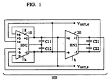
- FIG. 1 is a block diagram of an oscillator containing a balanced triple-input transconductor having a current clamp that is merged with a transconductance amplifier, in accordance with the invention.
- FIG. 2 is a schematic circuit diagram of the triple-input transconductor, in accordance with a specific embodiment of the invention.
- FIG. 1 shows an oscillator 100, in a balanced circuit configuration, comprising a balanced triple-input transconductor 10 and a balanced single-input transconductor 20, as well as a first pair of matched capacitors C11 and C12 and a second pair of matched capacitors C21 and C22.
- the triple-input transconductor 10 has three positive input points, +a, +b, and +c, and three negative input points -a, -b, and -c, as well as one positive output point +d and one negative output point -d. Note that because both transconductors 10 and 20 are balanced, the triple-input transconductor 10 has six physical input points, and the single-input transconductor 20 has two. That is to say, in a balanced circuit configuration the term "m-input transconductor" signifies 2m physical input points.
- the positive output point +d of the triple-input transconductor 10 is connected to feed the input points +a and -b, as well as to feed the input point +e of the single-input transconductor 20.
- this positive output point +d is connected to feed one of the capacitors C11 and a positive output terminal V OUT,P of the oscillator 100.
- the negative output point -d of the balanced triple-input transconductor 10 is connected to feed the capacitor C12, the negative input points -a and -e, the positive input point +b, and a negative output terminal V OUT,N of the oscillator 100.
- the overall output of the oscillator 100 is then equal to V OUT,N .
- the output point +f of the balanced single-input transconductor 20 is connected to feed the capacitor C21, as well as to feed the input point -c of the triple-input transconductor 10. Conversely, the output point -f of the balanced single-input transconductor 20 is connected to feed the capacitor C22, as well as to feed the input point +c of the triple-input transconductor 10.
- the single-input transconductor 20 delivers negative feedback to the triple-input transconductor 10.
- the triple-input transconductor 10 delivers both positive and negative input to itself. For example, the input point +a receives positive feedback from the positive output point +d, whereas the positive input point +b receives negative feedback from the negative output point -d.
- the triple-input transconductor 10 has another input point k, which is optional and which can be used to adjust the amplitude of oscillation.
- the triple-input transconductor 10 may have yet another input point g, or plurality thereof, for adjusting (tuning) the frequency of oscillation F of the oscillator 100.
- the single-input transconductor 20 may have another input point h, or a plurality thereof, for adjusting the frequency of oscillation by varying the transconductance of the transconductor 20.
- the oscillator 100 is a quadrature oscillator because the output of the transconductor 20 is out of phase with the output of the transconductor 10 by ⁇ /2 radians. This ⁇ /2 phase shift results from the integration of the voltage V(+e) - V(e) with respect to time by the transconductor 20 operating in combination with capacitors C21 and C22.
- the circuitry for implementing the triple-input transconductor 10 consists essentially of three balanced paths running from ⁇ a, ⁇ b, ⁇ c to ⁇ d, whereby input voltages V(+a), V(-a); V(+b), V(-b); V(+c), V(-c) applied to points ⁇ a, ⁇ b, ⁇ c, respectively, are converted into balanced currents I(+a), I(-a); I(+b), I(-b); and I(+c), I(-c); respectively.
- the circuitry for the conversion of V(+a) and V(-a) into I(+a) and I(-a), respectively advantageously is a linear transconductance amplifier path in which there is merged a current clamp--i.e., essentially a linear transconductance amplifier path in which, when the input voltage exceeds a predetermined amount, linearity ceases and the output current remains fixed.
- the circuitry for the conversion of V(+b) and V(-b) into I(+b) and I(-b), respectively, is a linear transconductance amplifier path, as is the circuitry for the conversion of V(+c) and V(-c) into I(+c) and I(-c), respectively.
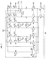
- a balanced triple-input transconductor circuit 200 represents a schematic drawing at the transistor level of a specific embodiment of the balanced triple-input transconductor 10 described above. Terminals and points that are similar in FIGS. 1 and 2 have been given the same reference labels.
- the circuit 200 is basically a complementary MOS (CMOS) circuit in which transistors M1, M2, M3, and M4 are n-channel transistors, whereas M5, M6,... through M23 are all p-channel.
- CMOS complementary MOS
- transconductance-tuning transistors MAB...MEB and MAC...MEC are p-channel transistors.
- Transistors MAB...MEB and MAC...MEC are all p-channel transistors, and serve to tune (vary) the transconductance, and hence damping, of inputs applied to points ⁇ b and ⁇ c, respectively, as more fully explained below.
- voltages g b1 ...g b5 are applied to the gate terminals of MAB...MEB, respectively, and voltages g c1 ...g c5 are applied to the gate terminals of MAC...MEC, respectively.
- Each of these voltages determine the on vs. off state of the respective transistor to which it is applied.
- the set of voltages g b1 ...g b5 determine the resistance between the source terminals of transistors M15 and M16--i.e., nodes N1 and N2--whereas the set of voltages g c1 ...g c5 determine the resistance between the source terminals of transistors M13 and M14.
- the resistance of each of these transistors MAB...MEB and MAC...MEC in the on state is in the range of about 5,000 to 20,000 ohms.
- the transistors MAB...MEB by virtue of their resistive damping, serve to control the amount of negative feedback from points ⁇ d to points ⁇ b.
- the transistors MAC...MEC control the amount of negative feedback from points ⁇ f (FIG. 1) to points ⁇ c.
- the transistors MAC...MEC serve to tune (vary) the oscillation frequency F, as more fully explained below.
- the amplitude of oscillation can be vied by applying a voltage to input point k, i.e., the gate terminal of M23: The amplitude of oscillations is proportional to the source-drain current flowing in the source-drain path of transistor M23.
- a positive power supply voltage VDD is supplied to the source terminals of M8, M7, M10, M9, M20, M19, and M23.
- a positive gate bias voltage BP2 is applied to the gate terminals of M8, M7, M10, M9, M20, and M19.
- Another positive gate bias voltage BP1 is applied to the gate terminals of M6, M5, M12, M11, M18 and M17.
- a gate bias voltage BN1 is applied to the gate terminals M4 and M3; and another gate bias voltage BN2 is applied to the gate terminals of M2 and M1.
- the source terminals of transistors M1 and M2 are connected to ground (negative power supply). These transistors are current sources. The amounts of current supplied by these sources are respectively equal to the sums of the four currents emanating from M3, M21, M15, M13 and M4, M22, M16, M14.
- the p-channel transistor-pair M9 and M11 form a cascode current source, as does each of the p-channel transistor-pairs M10 and M12, M7 and M5, M8 and M6, M19 and M17, and M20 and M18.
- Transistor M23 forms a simple tunable current source.
- the n-channel transistor-pair M1 and M3 also forms a cascode current source, as does the n-channel transistor-pair M2 and M4.
- VDD 5.0 volt
- BP2 3.7 volt
- BP1 3.1 volt
- BN1 1.7 volt
- BN2 1.1 volt
- each of the following is a matched pair: M1 and M2; M3 and M4; M5 and M6; M7 and M8; M9 and M10; M11 and M12; M13 and M14; M15 and M16; M17 and M18; M19 and M20; and M21 and M22.
- the transistors M21 and M22 act as current steering devices, while transistor M23 acts as a current source.
- this signal difference exceeds a certain level, the difference current is clamped--i.e., does not change, because all of the current flowing through transistor M23 flows either through M21 or M22.
- the transistors M21, M22, and M23 function together as a clamped linear amplifier path in which M23 is merged and acts as a clamp.
- the transistors in group MAB...MEB and in group MAC...MEG serve as resistors, typically five in each group. Each of their on-off states can be separately controlled by voltages g b1 ...g b5 and g c1 ...g c 5, respectively, applied to their gate terminals. These terminals correspond to the input point g(FIG. 1) of the counterpart transconductor 10.
- the set of transistors MAB...MEB supply a controllable resistance, as does the set of transistors MAC...MEC.
- the transconductance, and hence the reciprocal of the effective resistive damping, with respect to inputs at points ⁇ b is equal to 2/R.
- this transconductance can be adjusted (tuned).
- the resistance across the transistors MAC...MEC the transconductance, and hence resistive damping, with respect to inputs at ⁇ c can be tuned.
- the process of current summing by M1, and similarly by M2, operates as follows.
- the current through M21 increases, whereby the current through M3 decreases, because M1 is biased as a fixed current source.
- the remaining current stemming from transistors M5 and M7 flows out of point -d into capacitor C12.
- point +d draws current from C12. Similar considerations apply to signals applied to points ⁇ b and ⁇ c.
- transistors M5, M6, M7, M8, M9, M10, M11, M12, M17, M18, M19 or M20 operate in their respective saturation regions, primarily because of the presence of the two bias voltages BP1 and BP2 applied to transistors ( e.g. , M17, M19) whose source-drain paths are connected in series.
- the transconductors 10 and 20 need not be balanced--in which case the retained points are, for example, a, -b, -c, +d, +e, and +f.
- p- and n-channel MOS transistors can be everywhere interchanged.
Landscapes
- Amplifiers (AREA)
- Inductance-Capacitance Distribution Constants And Capacitance-Resistance Oscillators (AREA)
Applications Claiming Priority (2)
| Application Number | Priority Date | Filing Date | Title |
|---|---|---|---|
| US07/607,019 US5093634A (en) | 1990-10-31 | 1990-10-31 | Merged current clamp in triple-input transconductor, for use in oscillator |
| US607019 | 1990-10-31 |
Publications (3)
| Publication Number | Publication Date |
|---|---|
| EP0484031A2 true EP0484031A2 (de) | 1992-05-06 |
| EP0484031A3 EP0484031A3 (en) | 1992-12-02 |
| EP0484031B1 EP0484031B1 (de) | 1997-02-12 |
Family
ID=24430455
Family Applications (1)
| Application Number | Title | Priority Date | Filing Date |
|---|---|---|---|
| EP91309742A Expired - Lifetime EP0484031B1 (de) | 1990-10-31 | 1991-10-22 | Transkonduktanzverstärker mit drei Eingängen und verschmolzener Stromklemmschaltung, zur Verwendung in einem Oszillator |
Country Status (5)
| Country | Link |
|---|---|
| US (1) | US5093634A (de) |
| EP (1) | EP0484031B1 (de) |
| JP (1) | JPH077334A (de) |
| DE (1) | DE69124659T2 (de) |
| HK (1) | HK123397A (de) |
Families Citing this family (19)
| Publication number | Priority date | Publication date | Assignee | Title |
|---|---|---|---|---|
| US5212459A (en) * | 1991-11-12 | 1993-05-18 | Silicon Systems, Inc. | Linearized and delay compensated all CMOS VCO |
| US5155452A (en) * | 1991-11-12 | 1992-10-13 | Silicon Systems, Inc. | Linearized and delay compensated all CMOS VCO |
| US5185581A (en) * | 1992-03-26 | 1993-02-09 | Northern Telecom Limited | Differential amplifier and high frequency resonant circuits constructed therefrom |
| US5311088A (en) * | 1992-07-23 | 1994-05-10 | At&T Bell Laboratories | Transconductance cell with improved linearity |
| KR950003637B1 (ko) * | 1992-12-03 | 1995-04-17 | 삼성전자 주식회사 | 주파수 변조장치 |
| US5349304A (en) * | 1993-02-12 | 1994-09-20 | Sgs-Thomson Microelectronics, Inc. | Operational amplifier having multiple positive inputs |
| US5438288A (en) * | 1993-05-28 | 1995-08-01 | National Semiconductor Corporation | High differential output impedance setter |
| US5371475A (en) * | 1993-06-03 | 1994-12-06 | Northern Telecom Limited | Low noise oscillators and tracking filters |
| US5444421A (en) * | 1994-02-10 | 1995-08-22 | Racom Systems, Inc. | Low power consumption oscillator using multiple transconductance amplifiers |
| US5483195A (en) * | 1994-10-20 | 1996-01-09 | Northern Telecom Limited | Second generation low noise microwave voltage controlled oscillator |
| US5528179A (en) * | 1995-05-31 | 1996-06-18 | Texas Instruments Incorporated | Constant capacitance prgrammable transconductance input stage |
| JP3149797B2 (ja) * | 1996-09-18 | 2001-03-26 | 日本電気株式会社 | 電圧制御発振回路 |
| JP3449970B2 (ja) | 2000-07-21 | 2003-09-22 | 松下電器産業株式会社 | 相互コンダクタンス−容量フィルタシステム |
| US6727768B1 (en) | 2002-10-29 | 2004-04-27 | Institute Of Microelectronics | Relaxation CCO for PLL-based constant tuning of GM-C filters |
| US7728676B2 (en) | 2007-09-17 | 2010-06-01 | Atheros Communications, Inc. | Voltage-controlled oscillator with control range limiter |
| US8823450B2 (en) | 2012-07-19 | 2014-09-02 | Honeywell International Inc. | Multiple-output transconductance amplifier based instrumentation amplifier |
| US8729951B1 (en) | 2012-11-27 | 2014-05-20 | Freescale Semiconductor, Inc. | Voltage ramp-up protection |
| US9112462B2 (en) | 2013-05-15 | 2015-08-18 | Honeywell International Inc. | Variable-gain dual-output transconductance amplifier-based instrumentation amplifiers |
| US8917146B1 (en) * | 2014-02-18 | 2014-12-23 | King Fahd University Of Petroleum And Minerals | Current-controlled operational transconductance amplifier based sinusoidal oscillator circuit |
Family Cites Families (4)
| Publication number | Priority date | Publication date | Assignee | Title |
|---|---|---|---|---|
| NL8002666A (nl) * | 1980-05-09 | 1981-12-01 | Philips Nv | Operationele versterker. |
| US4760353A (en) * | 1988-01-04 | 1988-07-26 | Motorola, Inc. | Integrated gyrator oscillator |
| US4897612A (en) * | 1988-05-09 | 1990-01-30 | National Semiconductor Corporation | Operational transconductance amplifier with improved current source capability |
| GB2233513A (en) * | 1989-06-09 | 1991-01-09 | Philips Electronic Associated | Oscillators |
-
1990
- 1990-10-31 US US07/607,019 patent/US5093634A/en not_active Expired - Lifetime
-
1991
- 1991-10-22 EP EP91309742A patent/EP0484031B1/de not_active Expired - Lifetime
- 1991-10-22 DE DE69124659T patent/DE69124659T2/de not_active Expired - Fee Related
- 1991-10-28 JP JP3307112A patent/JPH077334A/ja active Pending
-
1997
- 1997-06-26 HK HK123397A patent/HK123397A/en not_active IP Right Cessation
Also Published As
| Publication number | Publication date |
|---|---|
| US5093634A (en) | 1992-03-03 |
| HK123397A (en) | 1997-09-12 |
| JPH077334A (ja) | 1995-01-10 |
| DE69124659T2 (de) | 1997-08-07 |
| EP0484031A3 (en) | 1992-12-02 |
| EP0484031B1 (de) | 1997-02-12 |
| DE69124659D1 (de) | 1997-03-27 |
Similar Documents
| Publication | Publication Date | Title |
|---|---|---|
| EP0484031B1 (de) | Transkonduktanzverstärker mit drei Eingängen und verschmolzener Stromklemmschaltung, zur Verwendung in einem Oszillator | |
| EP0455298B1 (de) | Elektrisch steuerbare Oszillatorschaltung und eine damit ausgerüstete, elektrisch steuerbare Filterschaltung | |
| US4374335A (en) | Tuneable I.C. active integrator | |
| KR100299740B1 (ko) | 필터회로 | |
| US5942929A (en) | Active phase splitter | |
| Chaturvedi et al. | Electronically tunable first-order filters and dual-mode multiphase oscillator | |
| US4117415A (en) | Bridge amplifiers employing complementary transistors | |
| US4760353A (en) | Integrated gyrator oscillator | |
| US6657502B2 (en) | Multiphase voltage controlled oscillator | |
| US6680645B2 (en) | Active filter circuit with operational amplifier | |
| US4388539A (en) | Integrated circuit comprising a plurality of voltage-current converters | |
| Soliman | Current mode CCII oscillators using grounded capacitors and resistors | |
| Sakul et al. | New resistorless current-mode quadrature oscillators using 2 CCCDTAs and grounded capacitors | |
| US8248112B2 (en) | Transconductance amplifier | |
| US4146849A (en) | Voltage controlled oscillator | |
| US7123083B2 (en) | Active filter circuit with operational amplifier | |
| US4518878A (en) | "All-pass" filter circuit including an integrable band-pass filter circuit | |
| JPH1093390A (ja) | 相互コンダクタンス増幅器および電圧制御発振器 | |
| US4122414A (en) | CMOS negative resistance oscillator | |
| Ozoguz et al. | Realization of high-Q bandpass filters using CCCIIs | |
| Nauta et al. | Automatic tuning of quality factors for VHF CMOS filters | |
| JP2001339275A (ja) | フィルタ回路とこれを用いた検波回路 | |
| Toyota et al. | A design of 1 V CMOS-OTA with wide input range | |
| Çiçekli et al. | Current operational amplifier based voltage-mode MOS-C all-pass filter and its application | |
| Theppota et al. | Electronically Controllable Multiphase Sinusoidal Oscillator Using VDGA-Based All Pass Filters |
Legal Events
| Date | Code | Title | Description |
|---|---|---|---|
| PUAI | Public reference made under article 153(3) epc to a published international application that has entered the european phase |
Free format text: ORIGINAL CODE: 0009012 |
|
| AK | Designated contracting states |
Kind code of ref document: A2 Designated state(s): DE FR GB IT |
|
| PUAL | Search report despatched |
Free format text: ORIGINAL CODE: 0009013 |
|
| AK | Designated contracting states |
Kind code of ref document: A3 Designated state(s): DE FR GB IT |
|
| 17P | Request for examination filed |
Effective date: 19930520 |
|
| RAP3 | Party data changed (applicant data changed or rights of an application transferred) |
Owner name: AT&T CORP. |
|
| GRAG | Despatch of communication of intention to grant |
Free format text: ORIGINAL CODE: EPIDOS AGRA |
|
| 17Q | First examination report despatched |
Effective date: 19960212 |
|
| GRAH | Despatch of communication of intention to grant a patent |
Free format text: ORIGINAL CODE: EPIDOS IGRA |
|
| GRAH | Despatch of communication of intention to grant a patent |
Free format text: ORIGINAL CODE: EPIDOS IGRA |
|
| GRAA | (expected) grant |
Free format text: ORIGINAL CODE: 0009210 |
|
| AK | Designated contracting states |
Kind code of ref document: B1 Designated state(s): DE FR GB IT |
|
| ET | Fr: translation filed | ||
| REF | Corresponds to: |
Ref document number: 69124659 Country of ref document: DE Date of ref document: 19970327 |
|
| ITF | It: translation for a ep patent filed | ||
| PLBE | No opposition filed within time limit |
Free format text: ORIGINAL CODE: 0009261 |
|
| STAA | Information on the status of an ep patent application or granted ep patent |
Free format text: STATUS: NO OPPOSITION FILED WITHIN TIME LIMIT |
|
| 26N | No opposition filed | ||
| PGFP | Annual fee paid to national office [announced via postgrant information from national office to epo] |
Ref country code: FR Payment date: 20010925 Year of fee payment: 11 |
|
| PGFP | Annual fee paid to national office [announced via postgrant information from national office to epo] |
Ref country code: GB Payment date: 20011008 Year of fee payment: 11 |
|
| PGFP | Annual fee paid to national office [announced via postgrant information from national office to epo] |
Ref country code: DE Payment date: 20011230 Year of fee payment: 11 |
|
| REG | Reference to a national code |
Ref country code: GB Ref legal event code: IF02 |
|
| PG25 | Lapsed in a contracting state [announced via postgrant information from national office to epo] |
Ref country code: GB Free format text: LAPSE BECAUSE OF NON-PAYMENT OF DUE FEES Effective date: 20021022 |
|
| PG25 | Lapsed in a contracting state [announced via postgrant information from national office to epo] |
Ref country code: DE Free format text: LAPSE BECAUSE OF NON-PAYMENT OF DUE FEES Effective date: 20030501 |
|
| GBPC | Gb: european patent ceased through non-payment of renewal fee |
Effective date: 20021022 |
|
| PG25 | Lapsed in a contracting state [announced via postgrant information from national office to epo] |
Ref country code: FR Free format text: LAPSE BECAUSE OF NON-PAYMENT OF DUE FEES Effective date: 20030630 |
|
| REG | Reference to a national code |
Ref country code: FR Ref legal event code: ST |
|
| PG25 | Lapsed in a contracting state [announced via postgrant information from national office to epo] |
Ref country code: IT Free format text: LAPSE BECAUSE OF NON-PAYMENT OF DUE FEES;WARNING: LAPSES OF ITALIAN PATENTS WITH EFFECTIVE DATE BEFORE 2007 MAY HAVE OCCURRED AT ANY TIME BEFORE 2007. THE CORRECT EFFECTIVE DATE MAY BE DIFFERENT FROM THE ONE RECORDED. Effective date: 20051022 |