EP0482265B1 - Method of forming a thin copper film by low temperature CVD - Google Patents
Method of forming a thin copper film by low temperature CVD Download PDFInfo
- Publication number
- EP0482265B1 EP0482265B1 EP90402924A EP90402924A EP0482265B1 EP 0482265 B1 EP0482265 B1 EP 0482265B1 EP 90402924 A EP90402924 A EP 90402924A EP 90402924 A EP90402924 A EP 90402924A EP 0482265 B1 EP0482265 B1 EP 0482265B1
- Authority
- EP
- European Patent Office
- Prior art keywords
- substrate
- copper
- copper film
- gas
- thin copper
- Prior art date
- Legal status (The legal status is an assumption and is not a legal conclusion. Google has not performed a legal analysis and makes no representation as to the accuracy of the status listed.)
- Expired - Lifetime
Links
- 239000010949 copper Substances 0.000 title claims description 73
- 229910052802 copper Inorganic materials 0.000 title claims description 69
- RYGMFSIKBFXOCR-UHFFFAOYSA-N Copper Chemical compound [Cu] RYGMFSIKBFXOCR-UHFFFAOYSA-N 0.000 title claims description 57
- 238000000034 method Methods 0.000 title claims description 24
- 239000000758 substrate Substances 0.000 claims description 69
- 239000007789 gas Substances 0.000 claims description 21
- UFHFLCQGNIYNRP-UHFFFAOYSA-N Hydrogen Chemical compound [H][H] UFHFLCQGNIYNRP-UHFFFAOYSA-N 0.000 claims description 16
- 229910052751 metal Inorganic materials 0.000 claims description 13
- 239000002184 metal Substances 0.000 claims description 13
- -1 copper halide Chemical class 0.000 claims description 12
- 239000000919 ceramic Substances 0.000 claims description 11
- 230000003197 catalytic effect Effects 0.000 claims description 9
- 230000004913 activation Effects 0.000 claims description 5
- 229910052736 halogen Inorganic materials 0.000 claims description 4
- 150000002367 halogens Chemical class 0.000 claims description 4
- 239000001257 hydrogen Substances 0.000 claims description 4
- 229910052739 hydrogen Inorganic materials 0.000 claims description 4
- 239000012433 hydrogen halide Substances 0.000 claims description 3
- 229910000039 hydrogen halide Inorganic materials 0.000 claims description 3
- 229910052721 tungsten Inorganic materials 0.000 claims description 3
- 229910001080 W alloy Inorganic materials 0.000 claims description 2
- 239000011347 resin Substances 0.000 claims description 2
- 229920005989 resin Polymers 0.000 claims description 2
- 229910001182 Mo alloy Inorganic materials 0.000 claims 1
- 229910001362 Ta alloys Inorganic materials 0.000 claims 1
- 239000011521 glass Substances 0.000 claims 1
- 239000010408 film Substances 0.000 description 29
- ORTQZVOHEJQUHG-UHFFFAOYSA-L copper(II) chloride Chemical compound Cl[Cu]Cl ORTQZVOHEJQUHG-UHFFFAOYSA-L 0.000 description 13
- LTPBRCUWZOMYOC-UHFFFAOYSA-N Beryllium oxide Chemical compound O=[Be] LTPBRCUWZOMYOC-UHFFFAOYSA-N 0.000 description 10
- PNEYBMLMFCGWSK-UHFFFAOYSA-N aluminium oxide Inorganic materials [O-2].[O-2].[O-2].[Al+3].[Al+3] PNEYBMLMFCGWSK-UHFFFAOYSA-N 0.000 description 8
- 229910021591 Copper(I) chloride Inorganic materials 0.000 description 7
- PMHQVHHXPFUNSP-UHFFFAOYSA-M copper(1+);methylsulfanylmethane;bromide Chemical compound Br[Cu].CSC PMHQVHHXPFUNSP-UHFFFAOYSA-M 0.000 description 7
- OXBLHERUFWYNTN-UHFFFAOYSA-M copper(I) chloride Chemical compound [Cu]Cl OXBLHERUFWYNTN-UHFFFAOYSA-M 0.000 description 7
- 239000010935 stainless steel Substances 0.000 description 7
- 229910001220 stainless steel Inorganic materials 0.000 description 7
- XEEYBQQBJWHFJM-UHFFFAOYSA-N Iron Chemical compound [Fe] XEEYBQQBJWHFJM-UHFFFAOYSA-N 0.000 description 6
- 229910021592 Copper(II) chloride Inorganic materials 0.000 description 5
- 229910045601 alloy Inorganic materials 0.000 description 5
- 239000000956 alloy Substances 0.000 description 5
- 230000008569 process Effects 0.000 description 5
- 230000015572 biosynthetic process Effects 0.000 description 4
- 238000000576 coating method Methods 0.000 description 4
- 239000007888 film coating Substances 0.000 description 4
- 238000009501 film coating Methods 0.000 description 4
- 238000010438 heat treatment Methods 0.000 description 4
- 238000005268 plasma chemical vapour deposition Methods 0.000 description 4
- 239000010453 quartz Substances 0.000 description 4
- VYPSYNLAJGMNEJ-UHFFFAOYSA-N silicon dioxide Inorganic materials O=[Si]=O VYPSYNLAJGMNEJ-UHFFFAOYSA-N 0.000 description 4
- 239000010409 thin film Substances 0.000 description 4
- 229910000831 Steel Inorganic materials 0.000 description 3
- 238000005229 chemical vapour deposition Methods 0.000 description 3
- 239000011248 coating agent Substances 0.000 description 3
- 229960003280 cupric chloride Drugs 0.000 description 3
- 229910052742 iron Inorganic materials 0.000 description 3
- 239000000463 material Substances 0.000 description 3
- 238000001465 metallisation Methods 0.000 description 3
- 239000010959 steel Substances 0.000 description 3
- 238000002441 X-ray diffraction Methods 0.000 description 2
- 238000004458 analytical method Methods 0.000 description 2
- 239000000460 chlorine Substances 0.000 description 2
- 229940045803 cuprous chloride Drugs 0.000 description 2
- 238000007772 electroless plating Methods 0.000 description 2
- 238000002149 energy-dispersive X-ray emission spectroscopy Methods 0.000 description 2
- 238000002474 experimental method Methods 0.000 description 2
- 238000004519 manufacturing process Methods 0.000 description 2
- 239000002245 particle Substances 0.000 description 2
- 229910000679 solder Inorganic materials 0.000 description 2
- 238000010183 spectrum analysis Methods 0.000 description 2
- PIGFYZPCRLYGLF-UHFFFAOYSA-N Aluminum nitride Chemical compound [Al]#N PIGFYZPCRLYGLF-UHFFFAOYSA-N 0.000 description 1
- ZAMOUSCENKQFHK-UHFFFAOYSA-N Chlorine atom Chemical compound [Cl] ZAMOUSCENKQFHK-UHFFFAOYSA-N 0.000 description 1
- UFHFLCQGNIYNRP-VVKOMZTBSA-N Dideuterium Chemical compound [2H][2H] UFHFLCQGNIYNRP-VVKOMZTBSA-N 0.000 description 1
- YZCKVEUIGOORGS-UHFFFAOYSA-N Hydrogen atom Chemical compound [H] YZCKVEUIGOORGS-UHFFFAOYSA-N 0.000 description 1
- 239000004642 Polyimide Substances 0.000 description 1
- 230000009471 action Effects 0.000 description 1
- 239000012790 adhesive layer Substances 0.000 description 1
- 230000002411 adverse Effects 0.000 description 1
- 239000012159 carrier gas Substances 0.000 description 1
- 239000003638 chemical reducing agent Substances 0.000 description 1
- 229910052801 chlorine Inorganic materials 0.000 description 1
- 238000007796 conventional method Methods 0.000 description 1
- 229910052593 corundum Inorganic materials 0.000 description 1
- 238000000151 deposition Methods 0.000 description 1
- 230000008021 deposition Effects 0.000 description 1
- 230000000694 effects Effects 0.000 description 1
- 238000010292 electrical insulation Methods 0.000 description 1
- 150000004820 halides Chemical class 0.000 description 1
- 150000002431 hydrogen Chemical class 0.000 description 1
- 230000010354 integration Effects 0.000 description 1
- 230000007246 mechanism Effects 0.000 description 1
- 229910001507 metal halide Inorganic materials 0.000 description 1
- 150000005309 metal halides Chemical class 0.000 description 1
- 150000002739 metals Chemical class 0.000 description 1
- 229910052750 molybdenum Inorganic materials 0.000 description 1
- 239000005022 packaging material Substances 0.000 description 1
- 231100000614 poison Toxicity 0.000 description 1
- 230000007096 poisonous effect Effects 0.000 description 1
- 229920001721 polyimide Polymers 0.000 description 1
- 239000011148 porous material Substances 0.000 description 1
- 239000000843 powder Substances 0.000 description 1
- 230000009467 reduction Effects 0.000 description 1
- 230000007261 regionalization Effects 0.000 description 1
- 238000005476 soldering Methods 0.000 description 1
- 238000004544 sputter deposition Methods 0.000 description 1
- 239000000126 substance Substances 0.000 description 1
- 229910052715 tantalum Inorganic materials 0.000 description 1
- 229920001187 thermosetting polymer Polymers 0.000 description 1
- WFKWXMTUELFFGS-UHFFFAOYSA-N tungsten Chemical compound [W] WFKWXMTUELFFGS-UHFFFAOYSA-N 0.000 description 1
- 239000010937 tungsten Substances 0.000 description 1
- 238000007738 vacuum evaporation Methods 0.000 description 1
- 229910001845 yogo sapphire Inorganic materials 0.000 description 1
Images
Classifications
-
- C—CHEMISTRY; METALLURGY
- C23—COATING METALLIC MATERIAL; COATING MATERIAL WITH METALLIC MATERIAL; CHEMICAL SURFACE TREATMENT; DIFFUSION TREATMENT OF METALLIC MATERIAL; COATING BY VACUUM EVAPORATION, BY SPUTTERING, BY ION IMPLANTATION OR BY CHEMICAL VAPOUR DEPOSITION, IN GENERAL; INHIBITING CORROSION OF METALLIC MATERIAL OR INCRUSTATION IN GENERAL
- C23C—COATING METALLIC MATERIAL; COATING MATERIAL WITH METALLIC MATERIAL; SURFACE TREATMENT OF METALLIC MATERIAL BY DIFFUSION INTO THE SURFACE, BY CHEMICAL CONVERSION OR SUBSTITUTION; COATING BY VACUUM EVAPORATION, BY SPUTTERING, BY ION IMPLANTATION OR BY CHEMICAL VAPOUR DEPOSITION, IN GENERAL
- C23C18/00—Chemical coating by decomposition of either liquid compounds or solutions of the coating forming compounds, without leaving reaction products of surface material in the coating; Contact plating
- C23C18/16—Chemical coating by decomposition of either liquid compounds or solutions of the coating forming compounds, without leaving reaction products of surface material in the coating; Contact plating by reduction or substitution, e.g. electroless plating
- C23C18/31—Coating with metals
- C23C18/38—Coating with copper
-
- C—CHEMISTRY; METALLURGY
- C23—COATING METALLIC MATERIAL; COATING MATERIAL WITH METALLIC MATERIAL; CHEMICAL SURFACE TREATMENT; DIFFUSION TREATMENT OF METALLIC MATERIAL; COATING BY VACUUM EVAPORATION, BY SPUTTERING, BY ION IMPLANTATION OR BY CHEMICAL VAPOUR DEPOSITION, IN GENERAL; INHIBITING CORROSION OF METALLIC MATERIAL OR INCRUSTATION IN GENERAL
- C23C—COATING METALLIC MATERIAL; COATING MATERIAL WITH METALLIC MATERIAL; SURFACE TREATMENT OF METALLIC MATERIAL BY DIFFUSION INTO THE SURFACE, BY CHEMICAL CONVERSION OR SUBSTITUTION; COATING BY VACUUM EVAPORATION, BY SPUTTERING, BY ION IMPLANTATION OR BY CHEMICAL VAPOUR DEPOSITION, IN GENERAL
- C23C16/00—Chemical coating by decomposition of gaseous compounds, without leaving reaction products of surface material in the coating, i.e. chemical vapour deposition [CVD] processes
- C23C16/44—Chemical coating by decomposition of gaseous compounds, without leaving reaction products of surface material in the coating, i.e. chemical vapour deposition [CVD] processes characterised by the method of coating
- C23C16/448—Chemical coating by decomposition of gaseous compounds, without leaving reaction products of surface material in the coating, i.e. chemical vapour deposition [CVD] processes characterised by the method of coating characterised by the method used for generating reactive gas streams, e.g. by evaporation or sublimation of precursor materials
- C23C16/4488—Chemical coating by decomposition of gaseous compounds, without leaving reaction products of surface material in the coating, i.e. chemical vapour deposition [CVD] processes characterised by the method of coating characterised by the method used for generating reactive gas streams, e.g. by evaporation or sublimation of precursor materials by in situ generation of reactive gas by chemical or electrochemical reaction
-
- C—CHEMISTRY; METALLURGY
- C23—COATING METALLIC MATERIAL; COATING MATERIAL WITH METALLIC MATERIAL; CHEMICAL SURFACE TREATMENT; DIFFUSION TREATMENT OF METALLIC MATERIAL; COATING BY VACUUM EVAPORATION, BY SPUTTERING, BY ION IMPLANTATION OR BY CHEMICAL VAPOUR DEPOSITION, IN GENERAL; INHIBITING CORROSION OF METALLIC MATERIAL OR INCRUSTATION IN GENERAL
- C23C—COATING METALLIC MATERIAL; COATING MATERIAL WITH METALLIC MATERIAL; SURFACE TREATMENT OF METALLIC MATERIAL BY DIFFUSION INTO THE SURFACE, BY CHEMICAL CONVERSION OR SUBSTITUTION; COATING BY VACUUM EVAPORATION, BY SPUTTERING, BY ION IMPLANTATION OR BY CHEMICAL VAPOUR DEPOSITION, IN GENERAL
- C23C16/00—Chemical coating by decomposition of gaseous compounds, without leaving reaction products of surface material in the coating, i.e. chemical vapour deposition [CVD] processes
- C23C16/06—Chemical coating by decomposition of gaseous compounds, without leaving reaction products of surface material in the coating, i.e. chemical vapour deposition [CVD] processes characterised by the deposition of metallic material
- C23C16/08—Chemical coating by decomposition of gaseous compounds, without leaving reaction products of surface material in the coating, i.e. chemical vapour deposition [CVD] processes characterised by the deposition of metallic material from metal halides
-
- C—CHEMISTRY; METALLURGY
- C23—COATING METALLIC MATERIAL; COATING MATERIAL WITH METALLIC MATERIAL; CHEMICAL SURFACE TREATMENT; DIFFUSION TREATMENT OF METALLIC MATERIAL; COATING BY VACUUM EVAPORATION, BY SPUTTERING, BY ION IMPLANTATION OR BY CHEMICAL VAPOUR DEPOSITION, IN GENERAL; INHIBITING CORROSION OF METALLIC MATERIAL OR INCRUSTATION IN GENERAL
- C23C—COATING METALLIC MATERIAL; COATING MATERIAL WITH METALLIC MATERIAL; SURFACE TREATMENT OF METALLIC MATERIAL BY DIFFUSION INTO THE SURFACE, BY CHEMICAL CONVERSION OR SUBSTITUTION; COATING BY VACUUM EVAPORATION, BY SPUTTERING, BY ION IMPLANTATION OR BY CHEMICAL VAPOUR DEPOSITION, IN GENERAL
- C23C16/00—Chemical coating by decomposition of gaseous compounds, without leaving reaction products of surface material in the coating, i.e. chemical vapour deposition [CVD] processes
- C23C16/06—Chemical coating by decomposition of gaseous compounds, without leaving reaction products of surface material in the coating, i.e. chemical vapour deposition [CVD] processes characterised by the deposition of metallic material
- C23C16/08—Chemical coating by decomposition of gaseous compounds, without leaving reaction products of surface material in the coating, i.e. chemical vapour deposition [CVD] processes characterised by the deposition of metallic material from metal halides
- C23C16/14—Deposition of only one other metal element
-
- C—CHEMISTRY; METALLURGY
- C23—COATING METALLIC MATERIAL; COATING MATERIAL WITH METALLIC MATERIAL; CHEMICAL SURFACE TREATMENT; DIFFUSION TREATMENT OF METALLIC MATERIAL; COATING BY VACUUM EVAPORATION, BY SPUTTERING, BY ION IMPLANTATION OR BY CHEMICAL VAPOUR DEPOSITION, IN GENERAL; INHIBITING CORROSION OF METALLIC MATERIAL OR INCRUSTATION IN GENERAL
- C23C—COATING METALLIC MATERIAL; COATING MATERIAL WITH METALLIC MATERIAL; SURFACE TREATMENT OF METALLIC MATERIAL BY DIFFUSION INTO THE SURFACE, BY CHEMICAL CONVERSION OR SUBSTITUTION; COATING BY VACUUM EVAPORATION, BY SPUTTERING, BY ION IMPLANTATION OR BY CHEMICAL VAPOUR DEPOSITION, IN GENERAL
- C23C16/00—Chemical coating by decomposition of gaseous compounds, without leaving reaction products of surface material in the coating, i.e. chemical vapour deposition [CVD] processes
- C23C16/44—Chemical coating by decomposition of gaseous compounds, without leaving reaction products of surface material in the coating, i.e. chemical vapour deposition [CVD] processes characterised by the method of coating
- C23C16/448—Chemical coating by decomposition of gaseous compounds, without leaving reaction products of surface material in the coating, i.e. chemical vapour deposition [CVD] processes characterised by the method of coating characterised by the method used for generating reactive gas streams, e.g. by evaporation or sublimation of precursor materials
- C23C16/452—Chemical coating by decomposition of gaseous compounds, without leaving reaction products of surface material in the coating, i.e. chemical vapour deposition [CVD] processes characterised by the method of coating characterised by the method used for generating reactive gas streams, e.g. by evaporation or sublimation of precursor materials by activating reactive gas streams before their introduction into the reaction chamber, e.g. by ionisation or addition of reactive species
Definitions
- the present invention relates to a method of forming a thin copper film on the surface of a substrate by means of low temperature CVD.
- a thin copper film can be formed on the surface of a ceramic substrate by metallization.
- a ceramic substrate such as an alumina substrate is widely used as a packaging material of an IC or as a substrate for mounting an IC.
- copper metallization is applied in general to the substrate surface so as to form a thin conductive film.
- An alumina (Al2O3) substrate is most widely used as a ceramic substrate.
- An alumina substrate exhibits excellent insulating properties, heat conductivity, resistance to chemicals, and mechanical strength, and is relatively cheap.
- marked progress is being made nowadays in the degree of integration, operating speed and output power of an IC, leading to a serious demand for a ceramic substrate with further improved heat-dissipating properties such as a substrate which is fully capable of acting as a heat sink.
- an alumina substrate normally has a heat conductivity of 10 to 35 W/mk and therefore fails to provide a sufficient heat sink function.
- Beryllia (BeO) substrates and aluminum nitride (AlN) substrates are known an ceramic substrates which function fully as heat sinks.
- beryllia substrates which have high heat conductivities ranging from 150 to 250 W/kb, are costly.
- BeO powder is poisonous which gives rise to difficulties in the manufacturing of beryllia substrates.
- aluminum nitride substrates have high heat conductivities on the order of 140 to 260 W/kb and have low manufacturing costs.
- AlN substrates exhibit excellent properties such as a low heat expansion coefficient, a high electrical insulation and a high mechanical strength. Thus, AlN substrates are expected to become more important in this field.
- the technique of forming a thin copper film may also be applied to the coating of the surface of a stainless alloy plate with a thin copper film.
- Stainless alloys are already widely used.
- the application of a thin copper film coating is expected to further promote the use of stainless alloys.
- the beautiful surface exhibited by a thin copper film coating makes stainless alloys suitable for use as a housing material, particularly, as an interior material and as an ornamental material.
- Stainless alloys exhibit poor solder wettability.
- solder wettability is markedly improved by the thin copper film coating, making it possible to use the stainless steel even in fields which require soldering.
- the thin copper film coating eliminates the problem of stainless steel of having high electrical resistance. It follows that stainless steel coated with a thin copper film exhibits both the excellent spring properties of the stainless steel and the low electrical resistance of the copper film when the coated stainless steel is used in various applications such is in switches, terminals of a dry cell casing, and the like.
- GB-A-574 737 discloses a process for producing metallic coatings on iron or steel, having in the iron or steel pores an adhesive layer containing a metal halide, by heating the impregnated iron or steel in a hydrogen environment.
- one object of the present invention is to provide a method of forming a thin copper film on a substrate surface by CVD in which the substrate is held at a relatively low temperature.
- a method of forming a thin copper film by CVD by (a) forming a gas stream containing a copper halide, following by introducing said gas beam into a CVD reaction chamber having a heated catalytic metal filament arranged therein, (b) introducing hydrogen gas into the CVD reaction chamber for activation of said hydrogen gas by the heated catalytic metal filament and (c) carrying out the reaction between the copper halide contained in the gas stream introduced in step (a) and the hydrogen activated in step (b) near the surface of a substrate having a temperature between 250°C and 1300°C arranged within the CVD reaction chamber so as to deposit a thin film of copper on the substrate surface.
- an especially preferred, but not limiting, way to form a gas stream containing a copper halide is to continuously supply a halogen gas (X2) or a hydrogen halide gas (HX) into a copper tube heated to, for example, about 1000°C. It is desirable to use a quartz furnace provided with an outer heater for heating the copper tube. The halogen gas or the hydrogen halide gas reacts with copper while flowing through the heated copper tube so as to form a copper halide (CuX or CuX2). Chlorine (Cl) is a desirable halogen. It is particularly desirable to pass HCl gas through the copper tube.
- CuCl or CuCl2 is formed within the halide, as shown below: Cu + HCl ⁇ CuCl + 1/2H2 Cu + 2HCl ⁇ CuCl2 + H2 Note that CuCl2 is converted into CuCl at about 993°C.
- the gas stream thus prepared is passed through a feed gas supply pipe into a CVD reaction chamber.
- a conventional reaction chamber used for such purposes can be used, except that a catalytic metal filament, which is described in detail in conjunction with step (b), should be positioned within the reaction chamber.
- step (a) Another technique can be employed in step (a).
- a copper halide prepared in advance is evaporated, and the resultant copper halide gas is supplied to the reaction chamber through a suitable pipe or nozzle. It is also possible to use a carrier gas which does not adversely affect the CVD reaction, if necessary.
- the hydrogen gas introduced into the CVD reaction chamber in step (b) serves to reduce the copper halide introduced therein in step (a).
- Molecular hydrogen H2 is believed to decompose into atomic hydrogen H by the action of the heated catalytic metal filament, as shown below: H2 ⁇ 2H
- the activation of the hydrogen gas makes it possible to deposit copper even on a substrate heated to a relatively low temperature, i.e., about 250°C to about 300°C.
- the activation step is most important in the present invention.
- the catalytic metal it is possible to use W, Ta, Mo, W alloy or the like as the catalytic metal. Also, it is desirable to heat the catalytic metal filament to about 800°C to about 2000°C, preferably, to 1000°C or more.
- step (a) the copper halide introduced in step (a) is decomposed or reduced by the hydrogen gas activated in step (b), and the resultant copper is deposited on the substrate surface.
- cuprous chloride and cupric chloride are reduced by activated hydrogen, as shown below: CuCl + H ⁇ Cu + HCl CuCl2 + 2H ⁇ Cu + 2HCl
- cupric chloride is likely to decompose into cuprous chloride.
- copper film formation occurs substantially by the reduction of cupric chloride.
- Step (c) is equivalent to the similar step in the conventional CVD reaction, except that the reducing agent of hydrogen gas is activated in the present invention. Since the hydrogen gas is activated, it is possible to deposit copper on the substrate surface so as to form a thin copper film, even if the substrate temperature is markedly lower than in conventional CVD. To be more specific, a thin copper film can be formed satisfactorily in the present invention, if the substrate is heated to 250°C to 1300°C in contrast to about 400°C to 1300°C required in the conventional CVD method.
- the thin copper film formation in the present invention under the substrate temperature of 250 to 300°C is of great significance in view of the fact that it has been impossible to form a thin copper film in the prior art at a substrate temperature of 300°C or less unless plasma CVD is employed.
- the pressure within the CVD reaction chamber should generally be 13.3 to 1.333 Pa (0.1 to 10.0 Torr) during the CVD reaction. Under a high pressure, a thick copper film can be obtained easily. However, large copper particles are deposited under a high pressure. For forming a thin film consisting of fine copper particles, it is desirable to set the pressure within the reaction chamber at 13.3 to 533.2 Pa (0.1 to 4.0 Torr), preferably, at 13.3 to 133.3 Pa (0.1 to 1.0 Torr).
- the substrate on which a thin copper film is to be formed is not particularly restricted in the present invention.
- a ceramic substrate such as an alumina substrate or an aluminum nitride substrate and a metal substrate such as a stainless steel substrate can be suitably used in the present invention.
- a thermosetting resin substrate such as a polyimide substrate because the heating temperature is relatively low in the present process.
- the CVD method of the present invention makes it possible to form a thin copper film on the surface of a substrate while keeping the substrate temperature at a level which is markedly lower than the temperatures employed in the conventional method. It follows that the method of the present invention produces prominent effects in various fields, e.g., in the metallization of ceramic packages and ceramic substrates for mounting an IC, and in the copper coating of a stainless steel.
- the present invention is directed to the formation of a copper thin film.
- the CVD method employed in the present invention is expected to be applicable to the formation of thin films of other metals.
- the apparatus shown in Figure 1 was used in the following examples.
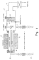
- the apparatus comprises a CVD reaction chamber 10 provided with a hydrogen gas supply pipe 12 and a discharge port 13.
- a tungsten filament 14 and a substrate heater 15 are arranged within the chamber 10.
- the filament 14 and the heater 15 are electrically energized.
- a substrate 16 such as a ceramic substrate, on which a thin copper film is to be formed, is positioned on the substrate heater 15.
- the apparatus also includes a quartz furnace 20 communicating with the reaction chamber 10.
- An outer heater 21 is disposed around the quartz furnace 20, and a copper pipe 22 is arranged in the furnace 20 such that one end portion of the pipe 22 is positioned outside the furnace 20.
- a HCl gas supply pipe 23 is connected to the end of the copper pipe 22 positioned outside the furnace 20, with the other end of the copper pipe 22 extending into the reaction chamber 10.
- a thin copper film was actually formed by using the apparatus described above.
- the substrate 16 was heated to 250°C.
- the copper pipe 22 and the W filament 14 were heated to 1000°C and 1400°C, respectively.
- the pressure within the chamber 10 was set at 133.3 Pa (1 Torr).
- HCl gas was allowed to flow through the copper pipe 22 at a flow rate of 10 sccm, while heating the quartz furnace 20 with the outer heater 21.
- the resultant gas stream containing copper chloride (CuCl and/or CuCl2) was introduced into the reaction chamber 10 through the copper halide supply pipe 11.
- hydrogen gas was also introduced into the chamber 10 at a flow rate of 10 sccm in order to be activated by the W filament 14.
- the copper chloride was reduced within the reaction chamber 10 by the activated hydrogen gas, with the result that copper was deposited on the surface of the substrate 16. The deposition was carried out for 120 minutes.
- a thin copper film was formed by the procedure described above on the surface of each of an alumina substrate (Example 1), an aluminum nitride substrate (Example 2) and a SUS 304 substrate (Example 3). A copper film about 1 ⁇ thick was formed in each of these examples.
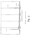
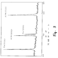
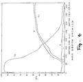
- the thin copper film formed on the surface of the aluminum nitride substrate in Example 2 was analyzed by EDAX spectrum analysis, X-ray analysis and Auger analysis. Figs. 2-4 show the results. These analytical results clearly indicate that the thin copper film formed by the method of the present invention can be fully used in various fields.
Landscapes
- Chemical & Material Sciences (AREA)
- General Chemical & Material Sciences (AREA)
- Chemical Kinetics & Catalysis (AREA)
- Engineering & Computer Science (AREA)
- Materials Engineering (AREA)
- Mechanical Engineering (AREA)
- Metallurgy (AREA)
- Organic Chemistry (AREA)
- Electrochemistry (AREA)
- Chemical Vapour Deposition (AREA)
- Internal Circuitry In Semiconductor Integrated Circuit Devices (AREA)
- Organic Low-Molecular-Weight Compounds And Preparation Thereof (AREA)
Description
- The present invention relates to a method of forming a thin copper film on the surface of a substrate by means of low temperature CVD.
- The technique of forming a thin copper film on the substrate surface is highly useful in various fields. For example, a thin copper film can be formed on the surface of a ceramic substrate by metallization. A ceramic substrate such as an alumina substrate is widely used as a packaging material of an IC or as a substrate for mounting an IC. When the ceramic substrate is used in such applications, it is necessary to form a wiring pattern on the substrate surface. For the wiring pattern formation, copper metallization is applied in general to the substrate surface so as to form a thin conductive film.
- An alumina (Al₂O₃) substrate is most widely used as a ceramic substrate. An alumina substrate exhibits excellent insulating properties, heat conductivity, resistance to chemicals, and mechanical strength, and is relatively cheap. On the other hand, marked progress is being made nowadays in the degree of integration, operating speed and output power of an IC, leading to a serious demand for a ceramic substrate with further improved heat-dissipating properties such as a substrate which is fully capable of acting as a heat sink. However, an alumina substrate normally has a heat conductivity of 10 to 35 W/mk and therefore fails to provide a sufficient heat sink function.
- Beryllia (BeO) substrates and aluminum nitride (AlN) substrates are known an ceramic substrates which function fully as heat sinks. However, beryllia substrates, which have high heat conductivities ranging from 150 to 250 W/kb, are costly. In addition, BeO powder is poisonous which gives rise to difficulties in the manufacturing of beryllia substrates. On the other hand, aluminum nitride substrates have high heat conductivities on the order of 140 to 260 W/kb and have low manufacturing costs. In addition, AlN substrates exhibit excellent properties such as a low heat expansion coefficient, a high electrical insulation and a high mechanical strength. Thus, AlN substrates are expected to become more important in this field.
- The technique of forming a thin copper film may also be applied to the coating of the surface of a stainless alloy plate with a thin copper film. Stainless alloys are already widely used. The application of a thin copper film coating is expected to further promote the use of stainless alloys. For example, the beautiful surface exhibited by a thin copper film coating makes stainless alloys suitable for use as a housing material, particularly, as an interior material and as an ornamental material. Stainless alloys exhibit poor solder wettability. However, solder wettability is markedly improved by the thin copper film coating, making it possible to use the stainless steel even in fields which require soldering. Further, the thin copper film coating eliminates the problem of stainless steel of having high electrical resistance. It follows that stainless steel coated with a thin copper film exhibits both the excellent spring properties of the stainless steel and the low electrical resistance of the copper film when the coated stainless steel is used in various applications such is in switches, terminals of a dry cell casing, and the like.
- For forming a thin copper film on a substrate surface, various methods are known to the art including, for example, vacuum evaporation, sputtering, electroless plating, CVD and plasma CVD. However, it is necessary to heat the substrate to a temperature of 400 to 1,300°C in each of these known methods except the electroless plating method and plasma CVD. Further, when it comes to the plasma CVD method, it is necessary to use a plasma generator which is very expensive. A need therefore continues to exist for an improved method of coating substrates with copper films.
- GB-A-574 737 discloses a process for producing metallic coatings on iron or steel, having in the iron or steel pores an adhesive layer containing a metal halide, by heating the impregnated iron or steel in a hydrogen environment.
- Accordingly, one object of the present invention is to provide a method of forming a thin copper film on a substrate surface by CVD in which the substrate is held at a relatively low temperature.
- Briefly, this object and other objects of the present invention as hereinafter will become more readily apparent and can be attained by a method of forming a thin copper film by CVD by (a) forming a gas stream containing a copper halide, following by introducing said gas beam into a CVD reaction chamber having a heated catalytic metal filament arranged therein, (b) introducing hydrogen gas into the CVD reaction chamber for activation of said hydrogen gas by the heated catalytic metal filament and (c) carrying out the reaction between the copper halide contained in the gas stream introduced in step (a) and the hydrogen activated in step (b) near the surface of a substrate having a temperature between 250°C and 1300°C arranged within the CVD reaction chamber so as to deposit a thin film of copper on the substrate surface.
- A more complete appreciation of the invention and many of the attendant advantages thereof will be readily obtained as the same becomes better understood by reference to the following detailed description when considered in connection with the accompanying drawings, wherein:
- Figure 1 shows the CVD apparatus used in the examples of the specification; and
- Figures 2 to 4 show the results of EDAX spectral analysis, X-ray analysis and Auger analysis, respectively, as obtained from a thin copper film formed by an embodiment of the present invention.
- For the first step of the present process, an especially preferred, but not limiting, way to form a gas stream containing a copper halide is to continuously supply a halogen gas (X₂) or a hydrogen halide gas (HX) into a copper tube heated to, for example, about 1000°C. It is desirable to use a quartz furnace provided with an outer heater for heating the copper tube. The halogen gas or the hydrogen halide gas reacts with copper while flowing through the heated copper tube so as to form a copper halide (CuX or CuX₂). Chlorine (Cl) is a desirable halogen. It is particularly desirable to pass HCl gas through the copper tube. When HCl is passed through the tube, CuCl or CuCl₂ is formed within the halide, as shown below:
Cu + HCl → CuCl + 1/2H₂
Cu + 2HCl → CuCl₂ + H₂
Note that CuCl₂ is converted into CuCl at about 993°C. - The gas stream thus prepared is passed through a feed gas supply pipe into a CVD reaction chamber. A conventional reaction chamber used for such purposes can be used, except that a catalytic metal filament, which is described in detail in conjunction with step (b), should be positioned within the reaction chamber.
- Another technique can be employed in step (a). In this method, a copper halide prepared in advance is evaporated, and the resultant copper halide gas is supplied to the reaction chamber through a suitable pipe or nozzle. It is also possible to use a carrier gas which does not adversely affect the CVD reaction, if necessary.
- In the second step of the process, the hydrogen gas introduced into the CVD reaction chamber in step (b) serves to reduce the copper halide introduced therein in step (a). Concerning the activation mechanism of the hydrogen gas introduced in step (b), molecular hydrogen H₂ is believed to decompose into atomic hydrogen H by the action of the heated catalytic metal filament, as shown below:
H₂ → 2H
The activation of the hydrogen gas makes it possible to deposit copper even on a substrate heated to a relatively low temperature, i.e., about 250°C to about 300°C. Naturally, the activation step is most important in the present invention. - It is possible to use W, Ta, Mo, W alloy or the like as the catalytic metal. Also, it is desirable to heat the catalytic metal filament to about 800°C to about 2000°C, preferably, to 1000°C or more.
- In the third step of the process, the copper halide introduced in step (a) is decomposed or reduced by the hydrogen gas activated in step (b), and the resultant copper is deposited on the substrate surface.
- For example, the cuprous chloride and cupric chloride are reduced by activated hydrogen, as shown below:
CuCl + H → Cu + HCl
CuCl₂ + 2H → Cu + 2HCl
As described previously, cupric chloride is likely to decompose into cuprous chloride. Thus, it may be reasonable to understand that copper film formation occurs substantially by the reduction of cupric chloride. - Step (c) is equivalent to the similar step in the conventional CVD reaction, except that the reducing agent of hydrogen gas is activated in the present invention. Since the hydrogen gas is activated, it is possible to deposit copper on the substrate surface so as to form a thin copper film, even if the substrate temperature is markedly lower than in conventional CVD. To be more specific, a thin copper film can be formed satisfactorily in the present invention, if the substrate is heated to 250°C to 1300°C in contrast to about 400°C to 1300°C required in the conventional CVD method. The thin copper film formation in the present invention under the substrate temperature of 250 to 300°C is of great significance in view of the fact that it has been impossible to form a thin copper film in the prior art at a substrate temperature of 300°C or less unless plasma CVD is employed.
- The pressure within the CVD reaction chamber should generally be 13.3 to 1.333 Pa (0.1 to 10.0 Torr) during the CVD reaction. Under a high pressure, a thick copper film can be obtained easily. However, large copper particles are deposited under a high pressure. For forming a thin film consisting of fine copper particles, it is desirable to set the pressure within the reaction chamber at 13.3 to 533.2 Pa (0.1 to 4.0 Torr), preferably, at 13.3 to 133.3 Pa (0.1 to 1.0 Torr).
- The substrate on which a thin copper film is to be formed is not particularly restricted in the present invention. As described previously, a ceramic substrate such as an alumina substrate or an aluminum nitride substrate and a metal substrate such as a stainless steel substrate can be suitably used in the present invention. It is also possible to use a thermosetting resin substrate such as a polyimide substrate because the heating temperature is relatively low in the present process.
- As described above in detail, the CVD method of the present invention makes it possible to form a thin copper film on the surface of a substrate while keeping the substrate temperature at a level which is markedly lower than the temperatures employed in the conventional method. It follows that the method of the present invention produces prominent effects in various fields, e.g., in the metallization of ceramic packages and ceramic substrates for mounting an IC, and in the copper coating of a stainless steel.
- The present invention is directed to the formation of a copper thin film. However, the CVD method employed in the present invention is expected to be applicable to the formation of thin films of other metals.
- Having generally described this invention, a further understanding can be obtained by reference to certain specific examples which are provided herein for purposes of illustration only and are not intended to be limiting unless otherwise specified.
- The apparatus shown in Figure 1 was used in the following examples. As shown in the drawing, the apparatus comprises a
CVD reaction chamber 10 provided with a hydrogengas supply pipe 12 and adischarge port 13. Atungsten filament 14 and asubstrate heater 15 are arranged within thechamber 10. Thefilament 14 and theheater 15 are electrically energized. Further, asubstrate 16 such as a ceramic substrate, on which a thin copper film is to be formed, is positioned on thesubstrate heater 15. - The apparatus also includes a
quartz furnace 20 communicating with thereaction chamber 10. Anouter heater 21 is disposed around thequartz furnace 20, and acopper pipe 22 is arranged in thefurnace 20 such that one end portion of thepipe 22 is positioned outside thefurnace 20. A HCl gas supply pipe 23 is connected to the end of thecopper pipe 22 positioned outside thefurnace 20, with the other end of thecopper pipe 22 extending into thereaction chamber 10. - A thin copper film was actually formed by using the apparatus described above. In this experiment, the
substrate 16 was heated to 250°C. Likewise, thecopper pipe 22 and theW filament 14 were heated to 1000°C and 1400°C, respectively. The pressure within thechamber 10 was set at 133.3 Pa (1 Torr). - To be more specific, HCl gas was allowed to flow through the
copper pipe 22 at a flow rate of 10 sccm, while heating thequartz furnace 20 with theouter heater 21. The resultant gas stream containing copper chloride (CuCl and/or CuCl₂) was introduced into thereaction chamber 10 through the copper halide supply pipe 11. On the other hand, hydrogen gas was also introduced into thechamber 10 at a flow rate of 10 sccm in order to be activated by theW filament 14. The copper chloride was reduced within thereaction chamber 10 by the activated hydrogen gas, with the result that copper was deposited on the surface of thesubstrate 16. The deposition was carried out for 120 minutes. - A thin copper film was formed by the procedure described above on the surface of each of an alumina substrate (Example 1), an aluminum nitride substrate (Example 2) and a SUS 304 substrate (Example 3). A copper film about 1 µ thick was formed in each of these examples.
- For comparison, a similar experiment was conducted in an attempt to form a thin copper film on the surface of each of an alumina substrate (Control 1), an aluminum nitride substrate (Control 2) and a SUS 304 substrate (Control 3), except that the
W filament 14 was not used in these Control cases. A thin copper film was not formed on the substrate in these Control cases. - Then, the thin copper film formed on the surface of the aluminum nitride substrate in Example 2 was analyzed by EDAX spectrum analysis, X-ray analysis and Auger analysis. Figs. 2-4 show the results. These analytical results clearly indicate that the thin copper film formed by the method of the present invention can be fully used in various fields.
Claims (4)
- A method of forming a thin copper film by CVD, comprising the steps of:(a) forming a gas stream containing a copper halide, followed by introducing said gas stream into a CVD reaction chamber having a heated catalytic metal filament arranged therein;(b) introducing hydrogen gas into the CVD reaction chamber for activation of said hydrogen gas by the heated catalytic metal filament; and(c) carrying out the reaction between the copper halide contained in the gas stream introduced in step (a) and the hydrogen activated in step (b) near the surface of a substrate having a temperature between 250°C and 1300°C, arranged within the CVD reaction chamber so as to deposit a thin copper film of copper on the substrate surface.
- The method according to Claim 1 or 2, wherein the substrate is selected from the group consisting of a ceramic substrate, a metal substrate, a glass substrate and a resin substrate.
- The method according to Claim 1, wherein the catalytic metal filament is formed of a metal selected from the group consisting of W, Ta, Mo and W alloy.
- The method according to claim 1, wherein the gas stream containing a copper halide is prepared by continuously supplying a halogen gas or a hydrogen halide gas to a heated copper tube.
Priority Applications (2)
| Application Number | Priority Date | Filing Date | Title |
|---|---|---|---|
| DE1990615820 DE69015820T2 (en) | 1990-10-18 | 1990-10-18 | Process for producing a copper thin layer by chemical vapor deposition at low temperature. |
| AT90402924T ATE116691T1 (en) | 1990-10-18 | 1990-10-18 | METHOD FOR PRODUCING A COPPER THIN FILM USING LOW TEMPERATURE CHEMICAL VAPOR DEPOSITION. |
Applications Claiming Priority (1)
| Application Number | Priority Date | Filing Date | Title |
|---|---|---|---|
| JP1264101A JP2856782B2 (en) | 1989-10-12 | 1989-10-12 | Method of forming copper thin film by low temperature CVD |
Publications (2)
| Publication Number | Publication Date |
|---|---|
| EP0482265A1 EP0482265A1 (en) | 1992-04-29 |
| EP0482265B1 true EP0482265B1 (en) | 1995-01-04 |
Family
ID=17398527
Family Applications (1)
| Application Number | Title | Priority Date | Filing Date |
|---|---|---|---|
| EP90402924A Expired - Lifetime EP0482265B1 (en) | 1989-10-12 | 1990-10-18 | Method of forming a thin copper film by low temperature CVD |
Country Status (5)
| Country | Link |
|---|---|
| US (1) | US5091209A (en) |
| EP (1) | EP0482265B1 (en) |
| JP (1) | JP2856782B2 (en) |
| KR (1) | KR910008164A (en) |
| CA (1) | CA2027285A1 (en) |
Families Citing this family (18)
| Publication number | Priority date | Publication date | Assignee | Title |
|---|---|---|---|---|
| FR2691984B1 (en) * | 1992-06-03 | 1995-03-24 | France Telecom | Method of depositing metal on a substrate and device for its implementation. |
| WO1998044164A1 (en) * | 1997-04-03 | 1998-10-08 | U.S. Department Of Commerce National Institute Of Standards And Technology | Method of forming metallic and ceramic thin film structures using metal halides and alkali metals |
| KR100313935B1 (en) * | 1998-06-30 | 2002-01-17 | 김영환 | The method for deposition of Cu in semiconductor |
| US6010749A (en) * | 1998-10-28 | 2000-01-04 | Goldman; Mark A. | Process for the production of volatile metal |
| US6245435B1 (en) | 1999-03-01 | 2001-06-12 | Moen Incorporated | Decorative corrosion and abrasion resistant coating |
| KR100367106B1 (en) * | 1999-03-05 | 2003-01-09 | 박보서 | Seat belt fitting type air bag |
| US7105434B2 (en) * | 1999-10-02 | 2006-09-12 | Uri Cohen | Advanced seed layery for metallic interconnects |
| US6610151B1 (en) * | 1999-10-02 | 2003-08-26 | Uri Cohen | Seed layers for interconnects and methods and apparatus for their fabrication |
| KR100458779B1 (en) * | 2000-03-27 | 2004-12-03 | 미츠비시 쥬고교 가부시키가이샤 | Method for forming metallic film and apparatus for forming the same |
| GB0108782D0 (en) * | 2001-04-07 | 2001-05-30 | Trikon Holdings Ltd | Methods and apparatus for forming precursors |
| JP3680029B2 (en) * | 2001-08-08 | 2005-08-10 | 三菱重工業株式会社 | Vapor growth method and vapor growth apparatus for metal thin film |
| US20030091739A1 (en) * | 2001-11-14 | 2003-05-15 | Hitoshi Sakamoto | Barrier metal film production apparatus, barrier metal film production method, metal film production method, and metal film production apparatus |
| US7659209B2 (en) | 2001-11-14 | 2010-02-09 | Canon Anelva Corporation | Barrier metal film production method |
| US7026057B2 (en) | 2002-01-23 | 2006-04-11 | Moen Incorporated | Corrosion and abrasion resistant decorative coating |
| EP1512772A1 (en) * | 2002-03-08 | 2005-03-09 | Mitsubishi Heavy Industries, Ltd. | Method and apparatus for production of metal film |
| JP2003318361A (en) * | 2002-04-19 | 2003-11-07 | Fujitsu Ltd | Semiconductor device and method of manufacturing the same |
| JP2009149998A (en) * | 2009-04-01 | 2009-07-09 | Canon Anelva Corp | Vapor deposition equipment for copper thin film |
| CN121260818B (en) * | 2025-12-04 | 2026-02-13 | 山东海化集团有限公司 | Preparation method of modified zinc-bromine flow battery carbon felt negative electrode and carbon felt negative electrode prepared by method |
Family Cites Families (6)
| Publication number | Priority date | Publication date | Assignee | Title |
|---|---|---|---|---|
| GB574737A (en) * | 1942-03-20 | 1946-01-18 | Robert Lionel Samuel | Improvements in or relating to metallic coatings on iron and steel |
| US4873119A (en) * | 1987-01-28 | 1989-10-10 | Chronar Corp. | Catalytic deposition of semiconductors |
| JPS63203772A (en) * | 1987-02-20 | 1988-08-23 | Hitachi Ltd | Vapor growth method for thin copper film |
| US4948623A (en) * | 1987-06-30 | 1990-08-14 | International Business Machines Corporation | Method of chemical vapor deposition of copper, silver, and gold using a cyclopentadienyl/metal complex |
| US4960072A (en) * | 1987-08-05 | 1990-10-02 | Ricoh Company, Ltd. | Apparatus for forming a thin film |
| DE3905297A1 (en) * | 1989-02-21 | 1990-08-23 | Siemens Ag | METHOD FOR PRODUCING POLYCRYSTALLINE SEMICONDUCTOR MATERIAL LAYERS BY PLASMA-EXCITED GAS PHASE DEPOSITION |
-
1989
- 1989-10-12 JP JP1264101A patent/JP2856782B2/en not_active Expired - Lifetime
-
1990
- 1990-10-10 CA CA002027285A patent/CA2027285A1/en not_active Abandoned
- 1990-10-11 US US07/596,001 patent/US5091209A/en not_active Expired - Fee Related
- 1990-10-11 KR KR1019900016131A patent/KR910008164A/en not_active Withdrawn
- 1990-10-18 EP EP90402924A patent/EP0482265B1/en not_active Expired - Lifetime
Also Published As
| Publication number | Publication date |
|---|---|
| EP0482265A1 (en) | 1992-04-29 |
| CA2027285A1 (en) | 1991-04-13 |
| US5091209A (en) | 1992-02-25 |
| JPH03126870A (en) | 1991-05-30 |
| JP2856782B2 (en) | 1999-02-10 |
| KR910008164A (en) | 1991-05-30 |
Similar Documents
| Publication | Publication Date | Title |
|---|---|---|
| US5091209A (en) | Method of forming a thin copper film by low temperture CVD | |
| US5173327A (en) | LPCVD process for depositing titanium films for semiconductor devices | |
| EP0936284B1 (en) | Method and apparatus for producing thin films | |
| Mårtensson et al. | Atomic layer epitaxy of copper on tantalum | |
| KR100691870B1 (en) | Chemical vapor deposition method of copper base film and mobilization precursor for it | |
| US5648123A (en) | Process for producing a strong bond between copper layers and ceramic | |
| EP0554246B1 (en) | Cvd of metal films from beta-diketonate complexes | |
| US4761345A (en) | Aluminum nitride substrate | |
| WO1996028586A1 (en) | Plasma enhanced chemical vapor deposition of titanium nitride using ammonia | |
| EP2017369A1 (en) | Chemical fluid deposition for the formation of metal and metal alloy films on patterned and unpatterned substrates | |
| US20090095425A1 (en) | Apparatus for the formation of a metal film | |
| EP0243723A2 (en) | A method for bonding a layer containing a refractory metal to a substrate | |
| JP3645682B2 (en) | CVD equipment for Cu film formation | |
| EP0425090A1 (en) | Film deposition method and apparatus | |
| US5358743A (en) | Selective and blanket chemical vapor deposition of Cu from (β-diketonate)Cu(L)n by silica surface modification | |
| JPS63203772A (en) | Vapor growth method for thin copper film | |
| EP0282285B1 (en) | A method of metallization for a nitride ceramic member | |
| KR19990053234A (en) | Chemical vapor deposition apparatus and copper thin film formation method using the same | |
| US5145714A (en) | Metal-organic chemical vapor deposition for repairing broken lines in microelectronic packages | |
| JP3031719B2 (en) | Diamond film deposition method on electroless plated nickel layer | |
| US6337290B1 (en) | Semiconductor device having fluorine-added carbon dielectric film and method of fabricating the same | |
| US5139856A (en) | Plated ceramic or glass substrate having undercoat | |
| KR100624351B1 (en) | Chemical vapor deposition method of metal film | |
| JP3320336B2 (en) | Nickel or nickel alloy deposition by iodide CVD | |
| JP2980645B2 (en) | Metal thin film forming method |
Legal Events
| Date | Code | Title | Description |
|---|---|---|---|
| PUAI | Public reference made under article 153(3) epc to a published international application that has entered the european phase |
Free format text: ORIGINAL CODE: 0009012 |
|
| 17P | Request for examination filed |
Effective date: 19901023 |
|
| AK | Designated contracting states |
Kind code of ref document: A1 Designated state(s): AT BE CH DE DK ES FR GB GR IT LI LU NL SE |
|
| 17Q | First examination report despatched |
Effective date: 19931027 |
|
| GRAA | (expected) grant |
Free format text: ORIGINAL CODE: 0009210 |
|
| AK | Designated contracting states |
Kind code of ref document: B1 Designated state(s): AT BE CH DE DK ES FR GB GR IT LI LU NL SE |
|
| PG25 | Lapsed in a contracting state [announced via postgrant information from national office to epo] |
Ref country code: IT Free format text: LAPSE BECAUSE OF FAILURE TO SUBMIT A TRANSLATION OF THE DESCRIPTION OR TO PAY THE FEE WITHIN THE PRE;WARNING: LAPSES OF ITALIAN PATENTS WITH EFFECTIVE DATE BEFORE 2007 MAY HAVE OCCURRED AT ANY TIME BEFORE 2007. THE CORRECT EFFECTIVE DATE MAY BE DIFFERENT FROM THE ONE RECORDED.SCRIBED TIME-LIMIT Effective date: 19950104 Ref country code: CH Effective date: 19950104 Ref country code: BE Effective date: 19950104 Ref country code: AT Effective date: 19950104 Ref country code: LI Effective date: 19950104 Ref country code: GR Free format text: LAPSE BECAUSE OF FAILURE TO SUBMIT A TRANSLATION OF THE DESCRIPTION OR TO PAY THE FEE WITHIN THE PRESCRIBED TIME-LIMIT Effective date: 19950104 Ref country code: ES Free format text: THE PATENT HAS BEEN ANNULLED BY A DECISION OF A NATIONAL AUTHORITY Effective date: 19950104 Ref country code: DK Effective date: 19950104 Ref country code: NL Effective date: 19950104 |
|
| REF | Corresponds to: |
Ref document number: 116691 Country of ref document: AT Date of ref document: 19950115 Kind code of ref document: T |
|
| REF | Corresponds to: |
Ref document number: 69015820 Country of ref document: DE Date of ref document: 19950216 |
|
| ET | Fr: translation filed | ||
| PG25 | Lapsed in a contracting state [announced via postgrant information from national office to epo] |
Ref country code: SE Effective date: 19950404 |
|
| REG | Reference to a national code |
Ref country code: CH Ref legal event code: PL |
|
| NLV1 | Nl: lapsed or annulled due to failure to fulfill the requirements of art. 29p and 29m of the patents act | ||
| PG25 | Lapsed in a contracting state [announced via postgrant information from national office to epo] |
Ref country code: GB Effective date: 19951018 |
|
| PG25 | Lapsed in a contracting state [announced via postgrant information from national office to epo] |
Ref country code: LU Free format text: LAPSE BECAUSE OF NON-PAYMENT OF DUE FEES Effective date: 19951031 |
|
| PLBE | No opposition filed within time limit |
Free format text: ORIGINAL CODE: 0009261 |
|
| STAA | Information on the status of an ep patent application or granted ep patent |
Free format text: STATUS: NO OPPOSITION FILED WITHIN TIME LIMIT |
|
| 26N | No opposition filed | ||
| GBPC | Gb: european patent ceased through non-payment of renewal fee |
Effective date: 19951018 |
|
| PGFP | Annual fee paid to national office [announced via postgrant information from national office to epo] |
Ref country code: FR Payment date: 20000911 Year of fee payment: 11 |
|
| PGFP | Annual fee paid to national office [announced via postgrant information from national office to epo] |
Ref country code: DE Payment date: 20000925 Year of fee payment: 11 |
|
| PG25 | Lapsed in a contracting state [announced via postgrant information from national office to epo] |
Ref country code: FR Free format text: LAPSE BECAUSE OF NON-PAYMENT OF DUE FEES Effective date: 20020628 |
|
| PG25 | Lapsed in a contracting state [announced via postgrant information from national office to epo] |
Ref country code: DE Free format text: LAPSE BECAUSE OF NON-PAYMENT OF DUE FEES Effective date: 20020702 |
|
| REG | Reference to a national code |
Ref country code: FR Ref legal event code: ST |