EP0481752A1 - Error correction code encoder and decoder - Google Patents
Error correction code encoder and decoder Download PDFInfo
- Publication number
- EP0481752A1 EP0481752A1 EP91309522A EP91309522A EP0481752A1 EP 0481752 A1 EP0481752 A1 EP 0481752A1 EP 91309522 A EP91309522 A EP 91309522A EP 91309522 A EP91309522 A EP 91309522A EP 0481752 A1 EP0481752 A1 EP 0481752A1
- Authority
- EP
- European Patent Office
- Prior art keywords
- code
- error correction
- correction code
- information
- parity
- Prior art date
- Legal status (The legal status is an assumption and is not a legal conclusion. Google has not performed a legal analysis and makes no representation as to the accuracy of the status listed.)
- Granted
Links
- 238000000034 method Methods 0.000 claims description 22
- 208000011580 syndromic disease Diseases 0.000 claims description 16
- 239000011159 matrix material Substances 0.000 claims description 10
- 230000005540 biological transmission Effects 0.000 claims description 9
- 238000010586 diagram Methods 0.000 description 12
- 230000008569 process Effects 0.000 description 10
- 239000000872 buffer Substances 0.000 description 4
- 230000000694 effects Effects 0.000 description 3
- 230000008859 change Effects 0.000 description 2
- 230000015654 memory Effects 0.000 description 2
- 230000003247 decreasing effect Effects 0.000 description 1
- 230000006872 improvement Effects 0.000 description 1
- 230000008707 rearrangement Effects 0.000 description 1
Images


Classifications
-
- G—PHYSICS
- G11—INFORMATION STORAGE
- G11B—INFORMATION STORAGE BASED ON RELATIVE MOVEMENT BETWEEN RECORD CARRIER AND TRANSDUCER
- G11B20/00—Signal processing not specific to the method of recording or reproducing; Circuits therefor
- G11B20/10—Digital recording or reproducing
- G11B20/18—Error detection or correction; Testing, e.g. of drop-outs
- G11B20/1833—Error detection or correction; Testing, e.g. of drop-outs by adding special lists or symbols to the coded information
-
- H—ELECTRICITY
- H03—ELECTRONIC CIRCUITRY
- H03M—CODING; DECODING; CODE CONVERSION IN GENERAL
- H03M13/00—Coding, decoding or code conversion, for error detection or error correction; Coding theory basic assumptions; Coding bounds; Error probability evaluation methods; Channel models; Simulation or testing of codes
- H03M13/27—Coding, decoding or code conversion, for error detection or error correction; Coding theory basic assumptions; Coding bounds; Error probability evaluation methods; Channel models; Simulation or testing of codes using interleaving techniques
-
- H—ELECTRICITY
- H03—ELECTRONIC CIRCUITRY
- H03M—CODING; DECODING; CODE CONVERSION IN GENERAL
- H03M13/00—Coding, decoding or code conversion, for error detection or error correction; Coding theory basic assumptions; Coding bounds; Error probability evaluation methods; Channel models; Simulation or testing of codes
- H03M13/29—Coding, decoding or code conversion, for error detection or error correction; Coding theory basic assumptions; Coding bounds; Error probability evaluation methods; Channel models; Simulation or testing of codes combining two or more codes or code structures, e.g. product codes, generalised product codes, concatenated codes, inner and outer codes
-
- H—ELECTRICITY
- H04—ELECTRIC COMMUNICATION TECHNIQUE
- H04N—PICTORIAL COMMUNICATION, e.g. TELEVISION
- H04N9/00—Details of colour television systems
- H04N9/79—Processing of colour television signals in connection with recording
- H04N9/87—Regeneration of colour television signals
- H04N9/88—Signal drop-out compensation
- H04N9/888—Signal drop-out compensation for signals recorded by pulse code modulation
Definitions
- the present invention relates to an error correction code encoder and decoder, and more particulayly to an encoder and decoder using a so-called product code as an error correction code in a system which transmits a code train via a transmission path such as a magnetic recording/reproducing path which may sometimes generate burst errors.
- interleave method is used to improve an error correction capability of a system having a transmission path such as a magnetic recording/reproducing path which may sometimes generate burst errors.
- data after being subject to error correction code encoding and constituting the same encoded block or same error correction code is distributedly sent to a transmission line.
- Such an interleave method used by a video VTR will be described by way of example.
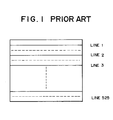
- Fig. 1 is a diagram used for explaining a video signal processed by a digital VTR.
- Fig. 1 there are shown horizontal scan lines including the first, second, ..., 525-th line.
- a video signal having 525 horizontal scan lines such as an NTSC signal is used.
- VTR digital video signals of one frame are divided into a predetermined number (P) of blocks.
- P predetermined number
- Each block is subject to error correction code encoding, and written in one track.
- P tracks are used for recording video signals of one frame.
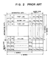
- Fig. 2 is a diagram illustrating error correction code encoded blocks.
- information data (information words) I11 to I ki is encoded by using such as Reed Solomon codes to provide inner codes in the horizontal direction and outer codes in the vertical direction, i.e., provide so-called product codes.
- inner and outer codes include three parity words (check bits) IP11 to 3m , and OP11 to OP 3k , respectively, and that each code can correct one word error.
- the order of recording data (order of data transmission) in a magnetic tape is the same as the direction of inner code encoding, i.e., in the order of I11, I12, I13, ..., I li , IP11, IP12, IP13, I21, I22, .... Therefore, burst errors caused by dropout by scratches or stains of a magnetic tape during a reproducing operation are consecutive in the inner code encoding direction.
- each outer or inner code can correct one word, burst errors of maximum one line or i words can be corrected by outer codes, but burst errors more than this cannot be corrected.
- data is encoded for each block.
- the encoded data is exchanged between blocks to record mixed data of a plurality of blocks in one track.
- data of two blocks is exchanged on the line unit basis.
- burst errors of maximum two lines can be corrected using outer codes because the reproducing process can be performed one line per each block.
- two tracks for the unit interleave process should not contain other burst errors or random errors. It can be said therefore that the above-described interleave method is very effective for improving the error correction capability without having a large redundancy if occurrence frequency of burst errors is low to a certain degree.
- Fig. 3 is a block diagram showing the brief arrangement of a conventional digital VTR which uses the interleave method.
- Information data inputted from an input terminal 300 is encoded on the block unit basis by an outer code encoding circuit 301 and inner code encoding circuit 302.
- the data is exchanged or interleaved in line unit or word unit at an interleave circuit 303 by using a memory.
- the interleave circuit 303 sequentially outputs data of a plurality of blocks to a recording circuit 304 which processes the data for magnetically recording it in a magnetic tape (recording medium) 310 serving as a transmission path.
- a signal picked up from the magnetic tape 310 is supplied to a reproducing circuit 305 to reproduce data.
- the reproduced data is processed by a de-inter-leave circuit 306 in the manner opposite to the interleave circuit 303, and sequentially outputted one line after another in units of block such as shown in Fig. 2.
- the outputted data is subject to error correction processes at an inner code decoding circuit 307 and outer code decoding circuit 308 using inner and outer codes.
- the error-corrected digital video signal is outputted from an output terminal 309.
- the above-described digital VTR requires address generators, memories, and the like, which are used for the interleave process only, resulting in an increase of hardware.
- the order of data before encoding is different from the order of data on a magnetic tape (on a transmission line). Therefore, a desired data order before error correction code encoding cannot be recorded (transmitted) as it is.
- a special reproducing mode of a digital VTR such as a high speed search which reproduces data while transporting a tape at a speed different from that when recording it, a particular data order is used for,allowing effective pixel reproduction.
- This particular data order of video signals changes if error correction code encoding is performed. It becomes therefore necessary to rearrange the data after error correction code encoding, or to determine a data order while considering such change in advance.
- an error correction code encoding device comprising:
- an error correction code decoding device comprising:
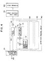
- Fig. 4 is a schematic diagram briefly showing the main part of a recording system of a digital VTR according to an embodiment of the present invention.
- reference numeral 100 represents an input terminal for a digital video signal. Like an ordinary television signal, data of each frame, each field, and each line is time sequentially inputted.
- Reference numeral 101 represents a special reproduction interleave circuit which changes a time sequential inputted digital video signal into a form suitable for a special reproduction such as high speed search.
- the structure of such a special reproduction interleave circuit can be realized using the teachings given in Japanese Patent Publication No. 63-55541 and U.S. Serial No. 317,430 filed on March 1, 1989.
- the structure of the circuit is not directly related to the present invention, so the detailed description thereof is omitted. It is assumed in this embodiment that the interleave circuit 101 interleaves data on the line unit basis.
- Reference numeral 140 represents an outer code encoding circuit which receives a data train from the special reproduction interleave circuit 101.
- the data train with outer code parities added by the outer code encoding circuit 140 is inputted to an inner code encoding circuit 150 which further adds inner code parities.
- Fig. 5 is a diagram showing encoded blocks used for explaining the error correction code encoding method used by VTR of this embodiment. Data on the first to 2k-th lines are sequentially inputted to the outer code encoding circuit 140 in this order. As shown in Fig. 5, it is assumed that three parity words are added as outer codes and as inner codes, respectively, and that each parity word can correct one word at the maximum.
- the data from the special reproduction interleave circuit 101 is inputted in parallel to a delay circuit 102, P0 parity calculation circuit 110, P1 parity calculation circuit 120, and P2 parity calculation circuit 130.
- parity calculation circuits 110, 120, and 130 are the same except that coefficients of generation matrix coefficient tables 112 are different.
- the three parity calculation circuits calculate three parity words.
- the operation of the parity calculation circuit will be described using the P0 parity calculation circuit 110 as an example.
- the information data supplied to the circuit 110 is inputted to a multiplier 111 on a Galois field.
- the generation matrix coefficient table 112 is constructed of a ROM and an address controller to sequentially output a coefficient of the generation matrix.
- the multiplier 111 multiplies the information data (word) by a coefficient outputted from the table 112, on a Galois field.
- An output of the multiplier 111 is supplied to an adder 113 constructed of an exclusive OR gate, and added to an addition result before two lines supplied from a two-line delay circuit 114.
- the adder 113 and two-line delay circuit 114 constitute an accumulator which accumulates the multiplication results between information words and coefficients at every second lines.
- outer codes different between odd lines and even lines are generated as shown in Fig. 5.
- outer code parity words P0 (OP11 to OP 1k shown in Fig. 5) are generated for odd line information codes
- outer code parity words P0 (OP′11 to OP′ 1k shown in Fig. 5) are generated for even line information codes.
- the generated parity words are stored in the delay circuit 114.
- Reference numeral 115 represents a buffer.
- the two-line delay circuits of the P1 and P2 parity calculation circuits 120 and 130 store therein outer code parity words P1 and P2 (OP21 to OP 2k , OP31 to OP 3k in Fig. 5) for odd line information codes and outer code parity words P1 and P2 (OP′21 to OP′ 2k , OP′31 to OP′31 in Fig. 5) for even line information codes.
- the delay circuit 102 provides the information data with a delay time corresponding to the time required for processing one word by the parity calculation circuit 110, 120, 130, and outputs the information data for the first to 2k-th lines in the order of having been inputted.
- the portion where inner code parity words are inserted is made undefined.
- the parity words stored in the two-line delay circuits of the parity calculation circuits 110, 120, and 130 are sequentially outputted via the buffers in the order of P0, P1, and P2 so that outer code parity words for six lines are outputted and added to respective 2k-lines information codes.
- An output of the outer code encoding circuit 140 is supplied to an inner code encoding circuit 150 and added with inner code parity words for each line, the inner code parity words being calculated in the well known manner.
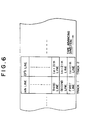
- the information words for 2k lines, 6k outer code parity words, and 6m inner code parity words are supplied to a recording circuit 160 sequentially for each line of the two sets of blocks shown in Fig. 5. These words are distributedly written on two tracks of a magnetic tape as shown in Fig. 6.
- each one word error can be corrected by using a corresponding one of outer codes.
- This improvement on error correction capability is the same as the conventional case wherein the dedicated interleave circuit 303 is additionally provided.
- the order of information codes is not-changed at all throughout the circuit path from the input stage of the outer code encoding circuit 140 to the input stage of the recording circuit 160, without influencing the order of information codes (video data) given by the specific reproduction interleave circuit 101.
- Various interleave rules can be considered for the specific reproduction interleave circuit 101.
- data is distributed in units of line to a plurality of tracks constituting one frame, and the data of one frame is thinned in units of line and uniformly distributed to each track.
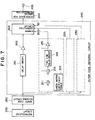
- Fig. 7 briefly shows an example of the arrangement of the main part of a reproducing recording system for code trains encoded as described above.
- Reference numeral 200 represents a reproducing circuit which reproduces code trains recorded on a magnetic tape shown in Fig. 6.
- the reproduced code train is supplied to an inner code decoding circuit 250 which calculates a syndrome of one line information words and three parity words so that an error is corrected by inner codes. Then, the code trains, i.e., information words with errors corrected by inner codes and outer code parity words, are supplied in parallel to a delay circuit 201, S0 syndrome calculation circuit 210, S1 syndrome calculation circuit 220, and S2 syndrome calculation circuit 230, one line after another.
- the structures of the syndrome calculation circuits 210, 220, and 230 are the same except that coefficients of check matrix coefficient tables 212 are different.
- the three syndrome calculation circuits calculate three syndromes S0, S1, and S2.
- the operation of the syndrome calculation circuit will be described using the S0 syndrome calculation circuit 210 as an example.
- the information data supplied to the syndrome calculation circuit 210 is inputted to a multiplier 111 on a Galois field.
- the check matrix coefficient table 212 is constructed of a ROM and an address controller to sequentially output a coefficient of the check matrix.
- the multiplier 211 multiplies the inputted word by a coefficient outputted from the table 212, on a Galois field.
- An output of the multiplier 211 is supplied to an adder 213 constructed of an exclusive OR gate, and added to an addition result before two lines supplied from a two-line delay circuit 214.
- the adder 213 and two-line delay circuit 214 constitute an accumulator which accumulates the multiplication results between information words, parity words and coefficients at every second lines.
- An error correction circuit 203 corrects errors of the information data supplied from the delay circuit 201 via a buffer 202, by using syndromes S0, S1, and S2 supplied from the syndrome calculation circuits 210, 220, and 230 via buffers 215, in the well known manner. If each outer code can correct one word, consecutive errors within two lines (2n words) generated by the reproducing circuit 200 can be corrected by the outer code decoding circuit 240.
- the first to 2k-th line information words are outputted from the outer code decoding circuit 240 in the order of having been reproduced, in the manner same as conventional.
- the order of the outputted information words is rearranged to recover the original order by a specific reproduction de-interleave circuit 204 which executes an rearrangement opposite to that of the specific reproduction interleave circuit 101, and outputted from an output terminal 205.
- a VTR having an encoder and decoder described above can improve the burst error correction capability of outer codes by using a different capacity of delay circuit's within the encoder and decoder.
- Error correction is performed within the processes of the encoder and decoder using error correction codes including outer and inner codes. Therefore, the hardware amounts of both the recording system (encoding system) and reproducing system (decoding system) will not become large while dispensing with a dedicated interleave circuit. Furthermore, such processes will not change the order of information code trains, without influencing a specific reproduction interleave.
- inner codes are disposed in the direction same as the direction of occurrence of burst errors. Namely, inner codes are added to consecutive information codes of i words (one line), and outer codes are obtained basing upon words derived at every second lines in the direction different from the first-mentioned direction. Instead, outer codes may be obtained basing upon words at each line, and inner codes may be obtained basing upon words derived at every second lines, with the similar advantageous effects being ensured. In other words, first and second error correction codes may be inner and outer codes, or vice versa.
- outer codes are obtained basing upon information words derived at every second lines, i.e., information words derived in the vertical direction of the data matrix shown in Fig. 5.
- Outer codes may be obtained basing upon information words derived in the oblique direction of the matrix, i.e., second codes (outer codes) may be obtained basing upon information words each derived from 2i consecutively transmitted information words, with the similar advantageous effects being ensured.
- outer code parity words are written concentrated on a magnetic tape at every second tracks. It is possible to distributedly allocate outer code parity words by increasing the capacity of the delay circuits 102 and 201 shown in Figs. 4 and 7. In this case, in addition to the above-described advantageous effects, errors at the reproducing circuit 200 can be reduced by decreasing the d.c. components of a code train.
Landscapes
- Engineering & Computer Science (AREA)
- Signal Processing (AREA)
- Physics & Mathematics (AREA)
- Probability & Statistics with Applications (AREA)
- Theoretical Computer Science (AREA)
- Multimedia (AREA)
- Error Detection And Correction (AREA)
Abstract
Description
- The present invention relates to an error correction code encoder and decoder, and more particulayly to an encoder and decoder using a so-called product code as an error correction code in a system which transmits a code train via a transmission path such as a magnetic recording/reproducing path which may sometimes generate burst errors.
- It is known that a so-called interleave method is used to improve an error correction capability of a system having a transmission path such as a magnetic recording/reproducing path which may sometimes generate burst errors. With this interleave method, data after being subject to error correction code encoding and constituting the same encoded block or same error correction code, is distributedly sent to a transmission line.
- Such an interleave method used by a video VTR will be described by way of example.
- Fig. 1 is a diagram used for explaining a video signal processed by a digital VTR. In Fig. 1, there are shown horizontal scan lines including the first, second, ..., 525-th line. In this example, a video signal having 525 horizontal scan lines such as an NTSC signal is used.
- In VTR, digital video signals of one frame are divided into a predetermined number (P) of blocks. Each block is subject to error correction code encoding, and written in one track. Namely, P tracks are used for recording video signals of one frame.
- Fig. 2 is a diagram illustrating error correction code encoded blocks. As shown in Fig. 2, information data (information words) I₁₁ to Iki is encoded by using such as Reed Solomon codes to provide inner codes in the horizontal direction and outer codes in the vertical direction, i.e., provide so-called product codes. In this example, it is assumed that inner and outer codes include three parity words (check bits) IP₁₁ to 3m, and OP₁₁ to OP3k, respectively, and that each code can correct one word error.
- The order of recording data (order of data transmission) in a magnetic tape is the same as the direction of inner code encoding, i.e., in the order of I₁₁, I₁₂, I₁₃, ..., Ili, IP₁₁, IP₁₂, IP₁₃, I₂₁, I₂₂, .... Therefore, burst errors caused by dropout by scratches or stains of a magnetic tape during a reproducing operation are consecutive in the inner code encoding direction.
- As described above, if each outer or inner code can correct one word, burst errors of maximum one line or i words can be corrected by outer codes, but burst errors more than this cannot be corrected.
- In order to improve the error correction capability, data is encoded for each block. The encoded data is exchanged between blocks to record mixed data of a plurality of blocks in one track. For example, in a simple case, data of two blocks is exchanged on the line unit basis. With such an arrangement, even if burst errors more than one line occur, burst errors of maximum two lines can be corrected using outer codes because the reproducing process can be performed one line per each block. However, in this case, two tracks for the unit interleave process should not contain other burst errors or random errors. It can be said therefore that the above-described interleave method is very effective for improving the error correction capability without having a large redundancy if occurrence frequency of burst errors is low to a certain degree.
- Fig. 3 is a block diagram showing the brief arrangement of a conventional digital VTR which uses the interleave method.
- Information data inputted from an
input terminal 300 is encoded on the block unit basis by an outercode encoding circuit 301 and innercode encoding circuit 302. The data is exchanged or interleaved in line unit or word unit at aninterleave circuit 303 by using a memory. Theinterleave circuit 303 sequentially outputs data of a plurality of blocks to arecording circuit 304 which processes the data for magnetically recording it in a magnetic tape (recording medium) 310 serving as a transmission path. - A signal picked up from the
magnetic tape 310 is supplied to a reproducingcircuit 305 to reproduce data. The reproduced data is processed by a de-inter-leave circuit 306 in the manner opposite to theinterleave circuit 303, and sequentially outputted one line after another in units of block such as shown in Fig. 2. The outputted data is subject to error correction processes at an innercode decoding circuit 307 and outercode decoding circuit 308 using inner and outer codes. The error-corrected digital video signal is outputted from anoutput terminal 309. - The above-described digital VTR requires address generators, memories, and the like, which are used for the interleave process only, resulting in an increase of hardware.
- Furthermore, the order of data before encoding is different from the order of data on a magnetic tape (on a transmission line). Therefore, a desired data order before error correction code encoding cannot be recorded (transmitted) as it is. In a special reproducing mode of a digital VTR, such as a high speed search which reproduces data while transporting a tape at a speed different from that when recording it, a particular data order is used for,allowing effective pixel reproduction. This particular data order of video signals changes if error correction code encoding is performed. It becomes therefore necessary to rearrange the data after error correction code encoding, or to determine a data order while considering such change in advance. In the former case, complicated processing is required, and moreover this processing is carried out with parity bits (words) being affixed so that data amount to be processed becomes bulky and the amount of hardware increases. Also in the latter case, complicated processing is required, a time required for data exchange may become longer, and the amount of hardware increases.
- In consideration of such circumstances, it is an object of the present invention to provide an error correction code encoder and decoder having a high error correction capability without increasing hardware so much.
- In order to achieve the above object of the present invention, there is presented an embodiment of an error correction code encoding device, comprising:
- (a) first encoding means for generating a first error correction code which is a first parity code added to a first code group having a predetermined number of consecutive information codes of a code sequence; and
- (b) second encoding means for generating a second error correction code which is a second parity code added to a second code group having information codes each derived from a first group among a plurality of consecutive code groups of the code sequence.
- There is also presented an embodiment of an error correction code decoding device, comprising:
- (a) first decoding means for decoding a first error correction code which is a first parity code added to a first code group having a predetermined number of consecutive information codes of a code sequence; and
- (b) second decoding means for decoding a second error correction code which is a second parity code added to a second code group having information codes each derived from a first group among a plurality of consecutive code groups of the code sequence.
- The other objects and advantages of the present invention will become more apparent from the following detailed description of the embodiments when read in connection with the accompanying drawings.
-
- Fig. 1 is a diagram used for explaining a video signal used in a digital VTR;
- Fig. 2 is a diagram showing error correction code encoded blocks of a conventional digital VTR;
- Fig. 3 is a block diagram showing the brief arrangement of a conventional digital VTR;
- Fig. 4 is a schematic diagram showing the main part of a recording system of a VTR according to an embodiment of the present invention;
- Fig. 5 is a diagram showing the structure of error correction code encoded blocks used for explaining an error correction code encoding method used by VTR shown in Fig. 4;
- Fig. 6 is a diagram showing a recording state of a tape used by VTR shown in Fig. 4; and
- Fig. 7 is a schematic diagram showing the main part of a reproducing system for VTR shown in Fig. 4.
- An embodiment of the present invention applied to a digital VTR will be described.
- Fig. 4 is a schematic diagram briefly showing the main part of a recording system of a digital VTR according to an embodiment of the present invention.
- In Fig. 4,
reference numeral 100 represents an input terminal for a digital video signal. Like an ordinary television signal, data of each frame, each field, and each line is time sequentially inputted. Reference numeral 101 represents a special reproduction interleave circuit which changes a time sequential inputted digital video signal into a form suitable for a special reproduction such as high speed search. The structure of such a special reproduction interleave circuit can be realized using the teachings given in Japanese Patent Publication No. 63-55541 and U.S. Serial No. 317,430 filed on March 1, 1989. The structure of the circuit is not directly related to the present invention, so the detailed description thereof is omitted. It is assumed in this embodiment that the interleave circuit 101 interleaves data on the line unit basis. -
Reference numeral 140 represents an outer code encoding circuit which receives a data train from the special reproduction interleave circuit 101. The data train with outer code parities added by the outercode encoding circuit 140 is inputted to an innercode encoding circuit 150 which further adds inner code parities. - Fig. 5 is a diagram showing encoded blocks used for explaining the error correction code encoding method used by VTR of this embodiment. Data on the first to 2k-th lines are sequentially inputted to the outer
code encoding circuit 140 in this order. As shown in Fig. 5, it is assumed that three parity words are added as outer codes and as inner codes, respectively, and that each parity word can correct one word at the maximum. - Referring to Fig. 4, the data from the special reproduction interleave circuit 101 is inputted in parallel to a
delay circuit 102, P0parity calculation circuit 110, P1parity calculation circuit 120, and P2parity calculation circuit 130. - The structures of the
parity calculation circuits - The operation of the parity calculation circuit will be described using the P0
parity calculation circuit 110 as an example. The information data supplied to thecircuit 110 is inputted to a multiplier 111 on a Galois field. The generation matrix coefficient table 112 is constructed of a ROM and an address controller to sequentially output a coefficient of the generation matrix. The multiplier 111 multiplies the information data (word) by a coefficient outputted from the table 112, on a Galois field. An output of the multiplier 111 is supplied to anadder 113 constructed of an exclusive OR gate, and added to an addition result before two lines supplied from a two-line delay circuit 114. Theadder 113 and two-line delay circuit 114 constitute an accumulator which accumulates the multiplication results between information words and coefficients at every second lines. - The above-described processes are executed for all information words I₁₁ to Iki and I′₁₁ to I′ki i.e., information words for 2k lines. Thus, outer codes different between odd lines and even lines are generated as shown in Fig. 5. outer code parity words P0 (OP₁₁ to OP1k shown in Fig. 5) are generated for odd line information codes, and outer code parity words P0 (OP′₁₁ to OP′1k shown in Fig. 5) are generated for even line information codes. The generated parity words are stored in the
delay circuit 114.Reference numeral 115 represents a buffer. - Similarly, the two-line delay circuits of the P1 and P2
parity calculation circuits - The
delay circuit 102 provides the information data with a delay time corresponding to the time required for processing one word by theparity calculation circuit - After the information data (2k x i words) of the two sets of blocks shown in Fig. 5 has been outputted, the parity words stored in the two-line delay circuits of the
parity calculation circuits - An output of the outer
code encoding circuit 140 is supplied to an innercode encoding circuit 150 and added with inner code parity words for each line, the inner code parity words being calculated in the well known manner. The information words for 2k lines, 6k outer code parity words, and 6m inner code parity words are supplied to arecording circuit 160 sequentially for each line of the two sets of blocks shown in Fig. 5. These words are distributedly written on two tracks of a magnetic tape as shown in Fig. 6. - With the error correction code encoding described above, even if burst errors of maximum two lines are present, each one word error can be corrected by using a corresponding one of outer codes. This improvement on error correction capability is the same as the conventional case wherein the
dedicated interleave circuit 303 is additionally provided. The order of information codes is not-changed at all throughout the circuit path from the input stage of the outercode encoding circuit 140 to the input stage of therecording circuit 160, without influencing the order of information codes (video data) given by the specific reproduction interleave circuit 101. Thus, it is not necessary to rearrange the order of k information codes after the error correction code encoding, making small the hardware amount of the specific reproduction interleave circuit 101. Various interleave rules can be considered for the specific reproduction interleave circuit 101. In general, data is distributed in units of line to a plurality of tracks constituting one frame, and the data of one frame is thinned in units of line and uniformly distributed to each track. - Fig. 7 briefly shows an example of the arrangement of the main part of a reproducing recording system for code trains encoded as described above.
Reference numeral 200 represents a reproducing circuit which reproduces code trains recorded on a magnetic tape shown in Fig. 6. - The reproduced code train is supplied to an inner
code decoding circuit 250 which calculates a syndrome of one line information words and three parity words so that an error is corrected by inner codes. Then, the code trains, i.e., information words with errors corrected by inner codes and outer code parity words, are supplied in parallel to adelay circuit 201, S0 syndrome calculation circuit 210, S1syndrome calculation circuit 220, and S2 syndrome calculation circuit 230, one line after another. - The structures of the
syndrome calculation circuits 210, 220, and 230 are the same except that coefficients of check matrix coefficient tables 212 are different. The three syndrome calculation circuits calculate three syndromes S0, S1, and S2. - The operation of the syndrome calculation circuit will be described using the S0 syndrome calculation circuit 210 as an example.
- The information data supplied to the syndrome calculation circuit 210 is inputted to a multiplier 111 on a Galois field. The check matrix coefficient table 212 is constructed of a ROM and an address controller to sequentially output a coefficient of the check matrix. The
multiplier 211 multiplies the inputted word by a coefficient outputted from the table 212, on a Galois field. An output of themultiplier 211 is supplied to anadder 213 constructed of an exclusive OR gate, and added to an addition result before two lines supplied from a two-line delay circuit 214. Theadder 213 and two-line delay circuit 214 constitute an accumulator which accumulates the multiplication results between information words, parity words and coefficients at every second lines. - The above-described processes are executed for all information words I₁₁ to Iki and I′₁₁ to I′ki and parity words OP₁₁ to OP′3k , OP₁₁ to OP′3k, for two lines. Thus, different syndromes S0 are calculated for odd lines and even lines.
- The above-described processes are carried out by the
syndrome calculation circuits 210, 220, and 230, so that syndromes S0, S1, and S2 for all outer codes are calculated, which are stored in two-line delay circuits within thecircuits 210, 220, and 230. - An
error correction circuit 203 corrects errors of the information data supplied from thedelay circuit 201 via abuffer 202, by using syndromes S0, S1, and S2 supplied from thesyndrome calculation circuits 210, 220, and 230 viabuffers 215, in the well known manner. If each outer code can correct one word, consecutive errors within two lines (2n words) generated by the reproducingcircuit 200 can be corrected by the outercode decoding circuit 240. - The first to 2k-th line information words are outputted from the outer
code decoding circuit 240 in the order of having been reproduced, in the manner same as conventional. The order of the outputted information words is rearranged to recover the original order by a specific reproductionde-interleave circuit 204 which executes an rearrangement opposite to that of the specific reproduction interleave circuit 101, and outputted from anoutput terminal 205. - A VTR having an encoder and decoder described above can improve the burst error correction capability of outer codes by using a different capacity of delay circuit's within the encoder and decoder. Error correction is performed within the processes of the encoder and decoder using error correction codes including outer and inner codes. Therefore, the hardware amounts of both the recording system (encoding system) and reproducing system (decoding system) will not become large while dispensing with a dedicated interleave circuit. Furthermore, such processes will not change the order of information code trains, without influencing a specific reproduction interleave.
- In the above embodiment, inner codes are disposed in the direction same as the direction of occurrence of burst errors. Namely, inner codes are added to consecutive information codes of i words (one line), and outer codes are obtained basing upon words derived at every second lines in the direction different from the first-mentioned direction. Instead, outer codes may be obtained basing upon words at each line, and inner codes may be obtained basing upon words derived at every second lines, with the similar advantageous effects being ensured. In other words, first and second error correction codes may be inner and outer codes, or vice versa.
- In the above embodiment, outer codes (second error correction codes) are obtained basing upon information words derived at every second lines, i.e., information words derived in the vertical direction of the data matrix shown in Fig. 5. Outer codes may be obtained basing upon information words derived in the oblique direction of the matrix, i.e., second codes (outer codes) may be obtained basing upon information words each derived from 2i consecutively transmitted information words, with the similar advantageous effects being ensured.
- Furthermore, in the above embodiment, as shown in Fig. 6, 3k outer code parity words are written concentrated on a magnetic tape at every second tracks. It is possible to distributedly allocate outer code parity words by increasing the capacity of the
delay circuits circuit 200 can be reduced by decreasing the d.c. components of a code train. - As described so far, according to the present invention, it is possible to realize an error correction code encoder and decoder having a high burst error correction capability without increasing the hardware amount to much extent.
Claims (16)
- An error correction code encoding device, comprising:(a) first encoding means for generating a first error correction code which is a first parity code added to a first code group having a predetermined number of consecutive information codes of a code sequence; and(b) second encoding means for generating a second error correction code which is a second parity code added to a second code group having information codes each derived from a first group among a plurality of consecutive code groups of said code sequence.
- A device according to claim 1, further comprising transmission means for transmitting said code sequence added with said first and second parity codes to a transmission path, without changing the order of information codes of said code sequence.
- A device according to claim 1, wherein said information code is video information, and the information amount of said first code group correpsonds to said video information of one horizontal scan line.
- A device according to claim 1, wherein said first error correction code is an inner code, and said second error correction code is an outer code.
- An error correction code encoding device, comprising:(a) first encoding means for generating a first error correction code which is a first parity word added to a first word group having i consecutive information words of a code sequence, where i is an integer 2 or larger; and(b) second encoding means for generating a second error correction code which is a second parity word added to a second word group having k information words each derived from (j x i) consecutive information word trains of said code sequence, where j and k are integers greater or equal to 2.
- A device according to claim 5, wherein said second encoding means includes a multiplier for multiplication of said information word by a generation matrix, and an accumulator including a delay circuit having a delay time longer than a period corresponding to (j - 1) x i words and an adder.
- An error correction code decoding device, comprising:(a) first decoding means for decoding a first error correction code which is a first parity code added to a first word group having i consecutive information words of a code sequence, where i is an integer greater or equal to 2; and(b) second decoding means for decoding a second error correction code which is a second parity code added to a second word group having k information words each derived from (j x i) consecutive information word trains of said code sequence, where j and k are integers greater or equal to 2.
- A device according to claim 7, further comprising reception means for receiving said code sequence having said information words added with said first and second parity words from a transmission line, and supplying said code sequence to said first or second decoding means without changing the order of said information words of said code sequence.
- A device according to claim 7, wherein said information word is video information, and the information amount of said first word group corresponds to said video information of one horizontal scan line.
- A device according to claim 5, wherein said first error correction code is an inner code, and said second error correction code is an outer code.
- A device according to claim 7, wherein said second decoding means includes a multiplier for multiplication of said information word and said parity word constituting said second error correction code by a generation matrix, and an accumulator including a delay circuit having a delay time longer than a period corresponding to (j - 1) x i words and an adder, and said second decoding means corrects an error using a syndrome outputted from said accumulator.
- An error correction code decoding device, comprising:(a) first decoding means for decoding a first error correction code which is a first parity code added to a first code group having a predetermined number of consecutive information codes of a code sequence; and(b) second decoding means for decoding a second error correction code which is a second parity code added to a second code group having information codes each derived from a first group among a plurality of consecutive code groups of said code sequence.
- An error correction code encoding device or method in which a first correction code and a second correction code are added to incoming data,
characterised in that
if the incoming data is arranged as an array the first correction code is based on consecutive data items in a line through the array in a first direction, and the second correction code is based on non-consecutive data items in a line through the array in a second direction. - A device or method according to claim 13 in which the second correction code is based on every n-th data item in a line through the array in the second direction, where n is an integer.
- An error correction code decoding device or method suitable for decoding data which has been error correction code encoded by a device or a method according to claim 13 or claim 14.
- An error correction code encoding and/or decoding device or method in which data is correction code encoded or decoded and re-ordered,
characterised in that
data is re-ordered before correction code encoding and after correction code decoding.
Applications Claiming Priority (2)
| Application Number | Priority Date | Filing Date | Title |
|---|---|---|---|
| JP279714/90 | 1990-10-17 | ||
| JP27971490A JPH04154222A (en) | 1990-10-17 | 1990-10-17 | Encoding and decoding equipment |
Publications (2)
| Publication Number | Publication Date |
|---|---|
| EP0481752A1 true EP0481752A1 (en) | 1992-04-22 |
| EP0481752B1 EP0481752B1 (en) | 1998-01-14 |
Family
ID=17614859
Family Applications (1)
| Application Number | Title | Priority Date | Filing Date |
|---|---|---|---|
| EP19910309522 Expired - Lifetime EP0481752B1 (en) | 1990-10-17 | 1991-10-16 | Error correction code encoder and decoder |
Country Status (3)
| Country | Link |
|---|---|
| EP (1) | EP0481752B1 (en) |
| JP (1) | JPH04154222A (en) |
| DE (1) | DE69128686T2 (en) |
Cited By (13)
| Publication number | Priority date | Publication date | Assignee | Title |
|---|---|---|---|---|
| EP0654910A1 (en) * | 1993-11-19 | 1995-05-24 | France Telecom | Method for detecting information bits processed by concatenated block codes |
| EP0817481A3 (en) * | 1996-07-03 | 1999-05-19 | Matsushita Electric Industrial Co., Ltd. | Reproducing method, reproducing apparatus and recording and reproducing apparatus using the same reproducing method, and recording medium having the same method recorded therein |
| US6065147A (en) * | 1996-08-28 | 2000-05-16 | France Telecom | Process for transmitting information bits with error correction coding, coder and decoder for the implementation of this process |
| EP0696799A4 (en) * | 1994-03-01 | 2000-06-28 | Sony Corp | METHOD AND APPARATUS FOR CODING DIGITAL SIGNALS, MEDIUM FOR RECORDING DIGITAL SIGNALS AND METHOD AND APPARATUS FOR DECODING DIGITAL SIGNALS |
| EP0673034A3 (en) * | 1994-03-19 | 2000-09-06 | Sony Corporation | Optical disk and method and apparatus for recording and then playing information back from that disk |
| US6122763A (en) * | 1996-08-28 | 2000-09-19 | France Telecom | Process for transmitting information bits with error correction coding and decoder for the implementation of this process |
| EP1067695A3 (en) * | 1999-07-08 | 2003-08-06 | Samsung Electronics Co., Ltd. | Error correction method for high density disc |
| EP1206041A3 (en) * | 2000-11-08 | 2003-11-26 | Kabushiki Kaisha Toshiba | Data processing method and apparatus, recording medium, reproducing method and apparatus |
| EP1182785A3 (en) * | 2000-08-25 | 2004-05-12 | Kabushiki Kaisha Toshiba | Data processing method and apparatus, recording medium, reproducing method and apparatus using the same method |
| US6903887B2 (en) * | 2002-01-03 | 2005-06-07 | International Business Machines Corporation | Multiple level (ML), integrated sector format (ISF), error correction code (ECC) encoding and decoding processes for data storage or communication devices and systems |
| USRE38802E1 (en) | 1994-03-19 | 2005-09-27 | Sony Corporation | Method for reproducing compressed information data from a disk using a spatial frequency less than the track pitch |
| KR101297060B1 (en) * | 2004-04-09 | 2013-08-19 | 에이저 시스템즈 엘엘시 | Multidimensional block encoder with sub-block interleaver and de-interleaver |
| CN113647516A (en) * | 2021-07-26 | 2021-11-16 | 中农科生物工程技术(苏州)有限公司 | Preparation method and application of streptozochytrium induced resistance protein LiiP1 |
Families Citing this family (2)
| Publication number | Priority date | Publication date | Assignee | Title |
|---|---|---|---|---|
| AU757231B2 (en) * | 1998-04-29 | 2003-02-06 | Koninklijke Philips Electronics N.V. | A method, device and carrier for encoding multiword information |
| CN114915380B (en) * | 2022-07-19 | 2022-09-30 | 中国科学院宁波材料技术与工程研究所 | CAN bus-based low-cost high-real-time automatic error correction communication system and method |
Citations (4)
| Publication number | Priority date | Publication date | Assignee | Title |
|---|---|---|---|---|
| GB2065416A (en) * | 1979-11-28 | 1981-06-24 | Sony Corp | Apparatus for recording digital video signals |
| EP0042121A1 (en) * | 1980-06-16 | 1981-12-23 | TELEFUNKEN Fernseh und Rundfunk GmbH | System for processing and transmitting PCM signals |
| EP0191410A2 (en) * | 1985-02-08 | 1986-08-20 | Hitachi, Ltd. | Method of transmitting digital data |
| EP0341851A2 (en) * | 1988-05-12 | 1989-11-15 | Digital Equipment Corporation | Method and apparatus for interleaved encoding |
-
1990
- 1990-10-17 JP JP27971490A patent/JPH04154222A/en active Pending
-
1991
- 1991-10-16 EP EP19910309522 patent/EP0481752B1/en not_active Expired - Lifetime
- 1991-10-16 DE DE1991628686 patent/DE69128686T2/en not_active Expired - Fee Related
Patent Citations (4)
| Publication number | Priority date | Publication date | Assignee | Title |
|---|---|---|---|---|
| GB2065416A (en) * | 1979-11-28 | 1981-06-24 | Sony Corp | Apparatus for recording digital video signals |
| EP0042121A1 (en) * | 1980-06-16 | 1981-12-23 | TELEFUNKEN Fernseh und Rundfunk GmbH | System for processing and transmitting PCM signals |
| EP0191410A2 (en) * | 1985-02-08 | 1986-08-20 | Hitachi, Ltd. | Method of transmitting digital data |
| EP0341851A2 (en) * | 1988-05-12 | 1989-11-15 | Digital Equipment Corporation | Method and apparatus for interleaved encoding |
Cited By (36)
| Publication number | Priority date | Publication date | Assignee | Title |
|---|---|---|---|---|
| FR2712760A1 (en) * | 1993-11-19 | 1995-05-24 | France Telecom | A method for transmitting information bits by applying concatenated block codes. |
| US5563897A (en) * | 1993-11-19 | 1996-10-08 | France Telecom | Method for detecting information bits processed by concatenated block codes |
| EP0654910A1 (en) * | 1993-11-19 | 1995-05-24 | France Telecom | Method for detecting information bits processed by concatenated block codes |
| EP0696799A4 (en) * | 1994-03-01 | 2000-06-28 | Sony Corp | METHOD AND APPARATUS FOR CODING DIGITAL SIGNALS, MEDIUM FOR RECORDING DIGITAL SIGNALS AND METHOD AND APPARATUS FOR DECODING DIGITAL SIGNALS |
| USRE38481E1 (en) | 1994-03-19 | 2004-03-30 | Sony Corporation | Method and apparatus for recording MPEG-compressed video data and compressed audio data on a disk |
| EP0673034A3 (en) * | 1994-03-19 | 2000-09-06 | Sony Corporation | Optical disk and method and apparatus for recording and then playing information back from that disk |
| USRE38802E1 (en) | 1994-03-19 | 2005-09-27 | Sony Corporation | Method for reproducing compressed information data from a disk using a spatial frequency less than the track pitch |
| EP0817481A3 (en) * | 1996-07-03 | 1999-05-19 | Matsushita Electric Industrial Co., Ltd. | Reproducing method, reproducing apparatus and recording and reproducing apparatus using the same reproducing method, and recording medium having the same method recorded therein |
| US6047398A (en) * | 1996-07-03 | 2000-04-04 | Matsushita Electric Industrial Co., Ltd. | Reproducing method, reproducing apparatus and recording and reproducing apparatus using the same reproducing method, and recording medium having the same method recorded therein |
| US6065147A (en) * | 1996-08-28 | 2000-05-16 | France Telecom | Process for transmitting information bits with error correction coding, coder and decoder for the implementation of this process |
| US6122763A (en) * | 1996-08-28 | 2000-09-19 | France Telecom | Process for transmitting information bits with error correction coding and decoder for the implementation of this process |
| US7370267B2 (en) | 1999-07-08 | 2008-05-06 | Samsung Electronics Co., Ltd. | Error correction method for high density disc |
| EP1067695A3 (en) * | 1999-07-08 | 2003-08-06 | Samsung Electronics Co., Ltd. | Error correction method for high density disc |
| US7739582B2 (en) | 1999-07-08 | 2010-06-15 | Samsung Electronics, Co., Ltd. | Error correction method for high density disc |
| US7401285B2 (en) | 1999-07-08 | 2008-07-15 | Samsung Electronics Co., Ltd. | Error correction method for high density disc |
| EP1555758A1 (en) * | 1999-07-08 | 2005-07-20 | Samsung Electronics Co., Ltd. | Error correction method for high density disc |
| US6931586B1 (en) | 1999-07-08 | 2005-08-16 | Samsung Electronics Co., Ltd. | Error correction method for high density disc |
| US7383491B2 (en) | 1999-07-08 | 2008-06-03 | Samsung Electronics Co., Ltd. | Error correction method for high density disc |
| US7350129B2 (en) | 2000-08-25 | 2008-03-25 | Kabushiki Kaisha Toshiba | Data processing method and apparatus, recording medium, reproducing method and apparatus using the same method |
| US7124345B2 (en) | 2000-08-25 | 2006-10-17 | Kabushiki Kaisha Toshiba | Data processing method and apparatus, recording medium, reproducing method and apparatus using the same method |
| US7302630B2 (en) | 2000-08-25 | 2007-11-27 | Kabushiki Kaisha Toshiba | Data processing method and apparatus, recording medium, reproducing method and apparatus using the same method |
| US7310763B2 (en) | 2000-08-25 | 2007-12-18 | Kabushiki Kaisha Toshiba | Data processing method and apparatus, recording medium, reproducing method and apparatus using the same method |
| US7346828B2 (en) | 2000-08-25 | 2008-03-18 | Kabushiki Kaisha Toshiba | Data processing method and apparatus, recording medium, reproducing method and apparatus using the same method |
| US7350128B2 (en) | 2000-08-25 | 2008-03-25 | Kabushiki Kaisha Toshiba | Data processing method and apparatus, recording medium, reproducing method and apparatus using the same method |
| EP1182785A3 (en) * | 2000-08-25 | 2004-05-12 | Kabushiki Kaisha Toshiba | Data processing method and apparatus, recording medium, reproducing method and apparatus using the same method |
| US7356754B2 (en) | 2000-08-25 | 2008-04-08 | Kabushiki Kaisha Toshiba | Data processing method and apparatus, recording medium, reproducing method and apparatus using the same method |
| US7363571B2 (en) | 2000-08-25 | 2008-04-22 | Kabushiki Kaisha Toshiba | Data processing method and apparatus, recording medium, reproducing method and apparatus using the same method |
| US7293218B2 (en) | 2000-08-25 | 2007-11-06 | Kabushiki Kaisha Toshiba | Data processing method and apparatus, recording medium, reproducing method and apparatus using the same method |
| US7370259B2 (en) | 2000-08-25 | 2008-05-06 | Kabushiki Kaisha Toshiba | Data processing method and apparatus, recording medium, reproducing method and apparatus using the same method |
| US7380196B2 (en) | 2000-08-25 | 2008-05-27 | Kabushiki Kaisha Toshiba | Data processing method and apparatus, recording medium, reproducing method and apparatus using the same method |
| US7380194B2 (en) | 2000-11-08 | 2008-05-27 | Kabushiki Kaisha Toshiba | Data processing method and apparatus, recording medium, reproducing method and apparatus |
| EP1206041A3 (en) * | 2000-11-08 | 2003-11-26 | Kabushiki Kaisha Toshiba | Data processing method and apparatus, recording medium, reproducing method and apparatus |
| US6907561B2 (en) | 2000-11-08 | 2005-06-14 | Kabushiki Kaisha Toshiba | Data processing method and apparatus, recording medium, reproducing method and apparatus |
| US6903887B2 (en) * | 2002-01-03 | 2005-06-07 | International Business Machines Corporation | Multiple level (ML), integrated sector format (ISF), error correction code (ECC) encoding and decoding processes for data storage or communication devices and systems |
| KR101297060B1 (en) * | 2004-04-09 | 2013-08-19 | 에이저 시스템즈 엘엘시 | Multidimensional block encoder with sub-block interleaver and de-interleaver |
| CN113647516A (en) * | 2021-07-26 | 2021-11-16 | 中农科生物工程技术(苏州)有限公司 | Preparation method and application of streptozochytrium induced resistance protein LiiP1 |
Also Published As
| Publication number | Publication date |
|---|---|
| JPH04154222A (en) | 1992-05-27 |
| DE69128686T2 (en) | 1998-05-07 |
| EP0481752B1 (en) | 1998-01-14 |
| DE69128686D1 (en) | 1998-02-19 |
Similar Documents
| Publication | Publication Date | Title |
|---|---|---|
| EP0061288B1 (en) | Digital television signal processing | |
| US5546409A (en) | Error correction encoding and decoding system | |
| EP0481752B1 (en) | Error correction code encoder and decoder | |
| US4393502A (en) | Method and apparatus for communicating digital information words by error-correction encoding | |
| US5636316A (en) | Picture signal digital processing unit | |
| US4791643A (en) | Single track orthogonal error correction system | |
| KR100250590B1 (en) | Encoding / Decoding Circuits and Digital Video Systems | |
| US4356564A (en) | Digital signal transmission system with encoding and decoding sections for correcting errors by parity signals transmitted with digital information signals | |
| JPS6342888B2 (en) | ||
| US5309450A (en) | Error correction coding method and apparatus for digital image information | |
| US6085348A (en) | Error correction code encoder and decoder | |
| JPH0520105A (en) | Digital data error correction device | |
| JPS61281722A (en) | Block transmission of digital information word | |
| EP0817481B1 (en) | Reproducing apparatus and recording and reproducing apparatus | |
| KR19990012450A (en) | 3D error correction method and device | |
| EP0405885A1 (en) | Recording device and reproducing device | |
| JPH07106983A (en) | Code generating method | |
| US6453439B1 (en) | Pseudo product code encoding and decoding apparatus and method | |
| JP3992443B2 (en) | Encoding method, decoding method, encoding circuit, decoding circuit, storage device, storage medium, and communication device | |
| JP2738659B2 (en) | Encoding method, encoding device, and decoding device | |
| KR200151025Y1 (en) | Digital Video Recorder | |
| JPH01159874A (en) | Pcm sound signal recording and reproducing device | |
| JPS592214A (en) | Digital recording/playback equipment | |
| JPH08212711A (en) | Data forming method, data reproducing method, data forming and reproducing method, data forming apparatus, data reproducing apparatus and disc | |
| JPH0628343B2 (en) | Product code decoding method |
Legal Events
| Date | Code | Title | Description |
|---|---|---|---|
| PUAI | Public reference made under article 153(3) epc to a published international application that has entered the european phase |
Free format text: ORIGINAL CODE: 0009012 |
|
| AK | Designated contracting states |
Kind code of ref document: A1 Designated state(s): DE ES FR GB IT NL |
|
| 17P | Request for examination filed |
Effective date: 19920909 |
|
| 17Q | First examination report despatched |
Effective date: 19950411 |
|
| GRAG | Despatch of communication of intention to grant |
Free format text: ORIGINAL CODE: EPIDOS AGRA |
|
| GRAH | Despatch of communication of intention to grant a patent |
Free format text: ORIGINAL CODE: EPIDOS IGRA |
|
| GRAH | Despatch of communication of intention to grant a patent |
Free format text: ORIGINAL CODE: EPIDOS IGRA |
|
| GRAA | (expected) grant |
Free format text: ORIGINAL CODE: 0009210 |
|
| AK | Designated contracting states |
Kind code of ref document: B1 Designated state(s): DE ES FR GB IT NL |
|
| PG25 | Lapsed in a contracting state [announced via postgrant information from national office to epo] |
Ref country code: IT Free format text: LAPSE BECAUSE OF FAILURE TO SUBMIT A TRANSLATION OF THE DESCRIPTION OR TO PAY THE FEE WITHIN THE PRESCRIBED TIME-LIMIT;WARNING: LAPSES OF ITALIAN PATENTS WITH EFFECTIVE DATE BEFORE 2007 MAY HAVE OCCURRED AT ANY TIME BEFORE 2007. THE CORRECT EFFECTIVE DATE MAY BE DIFFERENT FROM THE ONE RECORDED. Effective date: 19980114 Ref country code: NL Free format text: LAPSE BECAUSE OF FAILURE TO SUBMIT A TRANSLATION OF THE DESCRIPTION OR TO PAY THE FEE WITHIN THE PRESCRIBED TIME-LIMIT Effective date: 19980114 Ref country code: ES Free format text: THE PATENT HAS BEEN ANNULLED BY A DECISION OF A NATIONAL AUTHORITY Effective date: 19980114 |
|
| REF | Corresponds to: |
Ref document number: 69128686 Country of ref document: DE Date of ref document: 19980219 |
|
| ET | Fr: translation filed | ||
| NLV1 | Nl: lapsed or annulled due to failure to fulfill the requirements of art. 29p and 29m of the patents act | ||
| PLBE | No opposition filed within time limit |
Free format text: ORIGINAL CODE: 0009261 |
|
| STAA | Information on the status of an ep patent application or granted ep patent |
Free format text: STATUS: NO OPPOSITION FILED WITHIN TIME LIMIT |
|
| 26N | No opposition filed | ||
| REG | Reference to a national code |
Ref country code: GB Ref legal event code: IF02 |
|
| PGFP | Annual fee paid to national office [announced via postgrant information from national office to epo] |
Ref country code: DE Payment date: 20071031 Year of fee payment: 17 |
|
| PGFP | Annual fee paid to national office [announced via postgrant information from national office to epo] |
Ref country code: GB Payment date: 20071005 Year of fee payment: 17 Ref country code: FR Payment date: 20071022 Year of fee payment: 17 |
|
| GBPC | Gb: european patent ceased through non-payment of renewal fee |
Effective date: 20081016 |
|
| REG | Reference to a national code |
Ref country code: FR Ref legal event code: ST Effective date: 20090630 |
|
| PG25 | Lapsed in a contracting state [announced via postgrant information from national office to epo] |
Ref country code: DE Free format text: LAPSE BECAUSE OF NON-PAYMENT OF DUE FEES Effective date: 20090501 |
|
| PG25 | Lapsed in a contracting state [announced via postgrant information from national office to epo] |
Ref country code: FR Free format text: LAPSE BECAUSE OF NON-PAYMENT OF DUE FEES Effective date: 20081031 |
|
| PG25 | Lapsed in a contracting state [announced via postgrant information from national office to epo] |
Ref country code: GB Free format text: LAPSE BECAUSE OF NON-PAYMENT OF DUE FEES Effective date: 20081016 |