EP0480509A1 - Arrangement for supplying energy to a load, as well as a drive system and a sound reproduction system comprising such an arrangement - Google Patents
Arrangement for supplying energy to a load, as well as a drive system and a sound reproduction system comprising such an arrangement Download PDFInfo
- Publication number
- EP0480509A1 EP0480509A1 EP91202566A EP91202566A EP0480509A1 EP 0480509 A1 EP0480509 A1 EP 0480509A1 EP 91202566 A EP91202566 A EP 91202566A EP 91202566 A EP91202566 A EP 91202566A EP 0480509 A1 EP0480509 A1 EP 0480509A1
- Authority
- EP
- European Patent Office
- Prior art keywords
- signal
- arrangement
- load
- energy supply
- frequency
- Prior art date
- Legal status (The legal status is an assumption and is not a legal conclusion. Google has not performed a legal analysis and makes no representation as to the accuracy of the status listed.)
- Granted
Links
Images


Classifications
-
- H—ELECTRICITY
- H04—ELECTRIC COMMUNICATION TECHNIQUE
- H04R—LOUDSPEAKERS, MICROPHONES, GRAMOPHONE PICK-UPS OR LIKE ACOUSTIC ELECTROMECHANICAL TRANSDUCERS; DEAF-AID SETS; PUBLIC ADDRESS SYSTEMS
- H04R3/00—Circuits for transducers, loudspeakers or microphones
-
- H—ELECTRICITY
- H02—GENERATION; CONVERSION OR DISTRIBUTION OF ELECTRIC POWER
- H02P—CONTROL OR REGULATION OF ELECTRIC MOTORS, ELECTRIC GENERATORS OR DYNAMO-ELECTRIC CONVERTERS; CONTROLLING TRANSFORMERS, REACTORS OR CHOKE COILS
- H02P7/00—Arrangements for regulating or controlling the speed or torque of electric DC motors
- H02P7/03—Arrangements for regulating or controlling the speed or torque of electric DC motors for controlling the direction of rotation of DC motors
- H02P7/04—Arrangements for regulating or controlling the speed or torque of electric DC motors for controlling the direction of rotation of DC motors by means of a H-bridge circuit
Definitions
- the invention relates to an arrangement for supplying energy to a load in dependence on a binary signal comprising a low-frequency component and a strong high-frequency component having a predetermined frequency which load has a low-pass frequency characteristic, in a first energy supply state the arrangement being devised for supplying energy to the load by means of an electric quantity with a specific polarity, in a second energy supply state for supplying energy to the load by means of an electric quantity with a polarity opposite to the specific polarity and, in a third energy supply state for interrupting the energy supply to the load, the arrangement comprising a control circuit for alternately causing the arrangement to adopt different energy supply states according to a switching pattern determined by the binary signal.
- the invention likewise relates to a drive system comprising such an arrangement to energize an exciter coil of a motor of the drive system.
- the invention further relates to a sound reproduction system comprising the above arrangement to energize an electroacoustic converter.
- a drive system of the type mentioned above is known, for example, from DE-OS 25 58 571.
- a dc motor is supplied with energy by means of a so-called H-bridge in which, in a first energy supply state, the motor is energized by a dc voltage source through two diagonally opposite switches in the H-bridge. In the second energy supply state the motor is energized by the same dc voltage source through two different diagonally opposite switches of the H-bridge. In the third energy supply state the motor is short-circuited by means of two switches of the H-bridge.
- the control circuit receives two pulse-width modulated binary signals which are each other's inverse value apart from a mutual phase shift. The phase shift is such that the ascending edge of one binary signal coincides with the descending edge of the other binary signal.
- the switch control signals for causing the H-bridge to adopt one of the three energy supply states are derived from these two binary signals.
- the H-bridge is brought to the first or the second energy supply state depending on the sign of the difference between these signals. If the signal values of the two binary signals are equal, the H-bridge is made to adopt the third energy supply state in which the supply is interrupted.
- the motor is energized with a current largely determined by the dc voltage component of the binary signal, so that the power dissipation caused in the motor and switches by the high-frequency component of the binary signal is reduced considerably relative to energy supply with pulse-width modulated operating voltages, while no use is made of the third energy supply state.
- the drawback of the prior-art arrangement is, however, that deriving the control signals which denote this third energy supply state is extremely complex.
- control circuit comprises a rejection filter having a ternary output signal which filter is adjusted to the frequency of the strong signal component, and in that the three different output signal values determine the three energy supply states.
- the invention is also based on the recognition that the dissipation is largely caused by a strong high-frequency component in the supply pattern which component corresponds at least to a single high-frequency component in the binary signal. This component can easily be removed with the aid of the rejection filter.
- rejection filter is a first order filter, comprising a delay circuit for delaying the binary signal and a signal processing circuit for deriving from the two binary signals an output signal which is indicative of the sum of the two binary signals.
- rejection filters of this type produce a ternary output signal so that the control signals can be derived from the output signals in an extremely simple manner.
- the arrangement according to the invention is suitable for control circuits deriving energy supply states from a binary pulse-width modulated signal and also for control circuits deriving the three energy supply states from a pulse-density modulated signal while the positions of successive pulses are mutually shifted an integer number of uniform time intervals.
- the distance between the low-frequency component of the frequency spectrum and the strong high-frequency component is considerably larger than for the former type of control circuit. This is advantageous in that the high-frequency component in the energy supply of the load is strongly suppressed.
- the arrangement according to the invention is highly suitable for energizing exciter coils of motors in control systems. If the control system relates to a feedback digital control system, the energy supply arrangement in combination with the exciter coil operates as a digital-to-analog converter, which highly simplifies controlling the exciting motor from the digital control circuit.
- the arrangement according to the invention is also suitable for energizing an electroacoustic converter in a sound reproduction system wherein the audio information is available in digital form, for example, for reading a so-called compact disc or a so-called digital audio tape cassette.
- the load When a load having a low-pass frequency characteristic is supplied with energy, the load is often supplied with a high-frequency binary supply voltage having a low-frequency component and a high-frequency component. Due to the low-pass nature of the frequency characteristic, the current to flow through the load will mainly be determined by the low-frequency component of the supply voltage.
- Suitable binary values for supplying energy to the load are, for example, a binary pulse-density modulated signal Vd as is represented in Figure 2a, or a pulse-width modulated signal Vb as is represented in Figure 3a.
- the frequency spectrums of the respective signals Vd and Vb are given as illustrative examples in Figures 4 and 5.
- the signals Vd and Vb have two signal levels, that is to say, + E and -E.
- the signal Vd comprises a number of constant-width pulses, while successive pulses p are mutually shifted an integer number of uniform time intervals 7 .
- the dc voltage component of the signal Vd is determined by the number of pulses per unit of time.
- the signal comprises a strong high-frequency component having a frequency I/2 7 .
- Figure 4d shows the low-frequency component Hld and the strong high-frequency component Hhd plotted against frequency. It should be observed that in Figure 4d the frequency component Hld has only a single frequency. In reality the low-frequency component Hld has a spectrum of frequencies.
- the pulse-width modulated signal represented in Figure 5a has a pulse repetition rate of 1/8 7 .
- the width 7P of the pulse p' may assume a number of different values. In the represented example the pulses may assume eight different discrete widths, that is to say, 1 7 , 2 7 , ..., 8 7 .
- the dc voltage component of the signal Vlb is determined by the ratio of pulse-width T p to the duration of the time interval 8 7 . This ratio is often denoted by the English term of duty cycle.
- the signal Vlb includes a strong high-frequency component having a frequency I/8 7 .
- the low-frequency component Hlb of the signal Vlb and the high-frequency component Hhb are plotted against frequency f in Figure 5d.
- the high-frequency component has only a very limited effect on the strength of the current through a load when the load is supplied with energy with the above binary signals.
- This high-frequency component results in a high-frequency current component having a relatively low amplitude which current component, however, does cause unnecessary dissipation in the load. This dissipation may be reduced considerably by supplying the load with a ternary signal in which the high-frequency component is strongly suppressed.
- FIG. 3 An arrangement according to the invention with which a load 1 is supplied with energy with a ternary signal, is represented in Figure 3.
- the arrangement comprises a signal generation circuit 2 generating a pulse-width or pulse-density modulated logic signal having two distinguishable logic levels 0 and 1.
- a suitable pulse-density modulated logic signal Vld is represented in Figure 4a and a suitable pulse-width modulated logic signal Vlb is represented in Figure 5a.
- the signals Vld and Vlb are similar to Vd and Vb respectively.
- the logic signal generated by the signal generation circuit 2 is applied to a rejection filter 3 adjusted to the strong high-frequency signal component in the logic signal.
- the rejection filter 3 produces a ternary signal.
- a high signal level is then represented by an output signal Vh
- an intermediate level is represented by an output signal Vm
- a low level is represented by an output signal VI.
- the output signals Vh, Vm and VI are applied as control signals to a control circuit 4 to which the load 1 is connected.
- the control circuit 4 is of a type made to adopt an energy supply state in response to the current signal Vh in which state the load 1 is supplied with energy by means of an electric quantity with a first polarity.
- the load 1 is energized by means of an electric quantity with a polarity opposite to the first polarity.
- the control signal Vm the energy supply to the load is interrupted.
- FIG. 6 shows a first embodiment of the control circuit 4 for supplying energy to an inductive load 1', for example, an exciter coil of a motor or electroacoustic converter.
- the load 1' is connected to a voltage source 60 by means of a switch 61 responsive to the signal Vh.
- the load 1' is connected to a voltage source 62 by means of a switch 63 responsive to the control signal VI.
- the voltage of the voltage source 60 is such that when the switch 61 is closed, the load is energized with a voltage + E.
- the voltage of the voltage source 62 is opposite to that of a voltage source 60, so that the load is energized with a voltage -E when switch 63 is closed.
- control circuit shown in Figure 6 comprises another switch 64 controlled by the control signal Vm, for short-circuiting the load 1'.
- the load will be supplied with a voltage + E, a voltage -E or short-circuited respectively.
- the load 1' is supplied with a ternary signal in accordance with the output signals of the filter 3.
- FIG. 7 A second embodiment of the control circuit for supplying energy to the inductive load 1' is shown in Figure 7.
- This control circuit comprises a so-called H-bridge formed by a first circuit of a series combination of two switches 70 and 72, connected to a voltage source 74, and a second circuit of a series combination of switches 71 and 73 likewise connected to the voltage source 74.
- the switches 70, ..., 73 are responsive to four control signals Vs1, ..., Vs4 derived from the control signals Vh, Vm and VI by a suitable logic circuit 75.
- the logic circuit 75 is of a customary type which generates, in response to the control signals Vh, the control signals Vs1 and Vs3 for closing the switches 70 and 73, generates, in response to the control signal VI, the control signals Vs2 and Vs4 for closing the switches 71 and 72 and generates, in response to the control signal Vm the control signals Vs3 and Vs4 for closing the switches 72 and 73.
- the load 1' is again supplied with a ternary voltage having the voltage levels + E, -E and 0 which levels correspond to the ternary output signal of the rejection filter 3.
- Figure 8 shows an embodiment of the control circuit 4 for supplying energy to a capacitive load 1" from two controllable current sources 80 and 81 having a strength I.
- the current sources 80 and 81 are connected in parallel across the load 1", while the polarities of the current sources are each other's opposite.
- the current sources 80 and 81 are controlled by the respective output signals Vh and VI. In this fashion the load 1" is supplied with a ternary supply current having the current values + I, -I and 0, which supply current corresponds to the ternary output signal of the rejection filter 3.
- the rejection filter used may basically be any rejection filter. In the case where the number of signal levels at the output exceeds three, this output signal can be converted into a ternary signal by implementing customary quantization techniques.
- a rejection filter is used consisting of a delay element for delaying the input signal and a signal processing circuit, for example, an adder, which derives from the input signal and the delayed input signal signals denoting that the two input signals have a logic value 1, a logic value 0 or that the logic values of the two input signals are unequal.
- FIG 9 shows an embodiment of the rejection filter 3 for eliminating the strong high-frequency component Hhd in the pulse-density modulated signal Vld.
- the filter comprises a delay element 90 for delaying the input signal Vld over the time interval 7 .
- the delay element 90 is preferably to comprise a flip-flop which is controlled in synchronism with the input signal Vld by means of a clock signal at a rate of I/ 7 .
- the delay element 90 applies a delayed signal Vld' to an adder circuit 91 where the delayed signal Vld' is added to the signal Vld.
- the result of the addition performed by the adder circuit 91 is a ternary signal represented by a 2-bit output signal Vop.
- Figures 4b and 4c show the delayed signal Vld' and the result Res of the addition represented by the signal Vop, plotted against time.
- the high, intermediate and low signal levels are to be distinguished by the respective levels 0,1 and 2 respectively.
- the 4-out-of-2 decoder 92 the 2-bit signal is converted into the signals Vh, Vm and VI.
- the control circuits shown in Figures 6 and 7 are used for the energy supply, the three levels 0, 1 , 2 correspond to the supply voltages -E, 0, + E.
- the three levels 0, 1, 2 correspond to the supply currents -I, 0, + I.
- the binary pulse-density signal Vld is converted into a ternary supply signal from which the high-frequency component having a frequency I/ 7 is eliminated. This avoids unnecessary dissipation due to this frequency component, both in the control circuit 4 and in the load 1.
- the three control signals VI, Vm and Vh are derived from the signals Vld and Vld' by means of a combination of the adder circuit 91 and a 4-out-of-2 decoder 92.
- this derivation can also be performed with different logic circuits, for example, with gate circuits generating the signals Vh, Vm and VI for the different combinations of logic values of the signals Vld and Vld'.
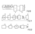
- Figure 10 shows an embodiment of the rejection filter for elimination of the frequency component Hhb having a frequency 1/8 7 in the pulse-width modulated signal Vhb.
- This embodiment comprises a delay element 100 for delaying the signal Vlb over a time interval 4 7 .
- the delay element 100 preferably comprises a shift register controlled in synchronism with the signal Vlb by means of a clock signal having a frequency I/ 7 .
- control signals Vh, Vm and VI are derived with the aid of the adder circuit 91 and the 4-out-of-2 decoder 92 in a similar fashion to that of the embodiment 9.
- FIGS 5b and 5c show the delayed signal Vlb' and the result Res' of the addition of Vlb and Vlb', plotted against time t.
- the result Res' again corresponds to the ternary supply signal obtained by means of the control circuit 4 in response to the signals Vh, Vm and VI. From this ternary signal the frequency component having the frequency 1/8 7 is eliminated so that the dissipation in the load 1 and the control circuit 4 induced by the frequency component Hhb in the binary pulse-width modulated signal Vlt is avoided.
- the energy supply arrangement according to the invention is pre-eminently suitable for energizing exciter coils of motors in position-servo systems such as, for example, a track-following servo system to be used in optical record and detection devices.
- position-servo systems such as, for example, a track-following servo system to be used in optical record and detection devices.
- the motor is disposed around a central position which means that the motor is supplied with relatively low supply voltages. Without the strong high-frequency component being filtered, the contribution of this component to the overall energy dissipated in the motor is large.
- FIG 11 shows an embodiment of a servo system comprising an energy supply arrangement according to the invention.
- a digital control circuit 110 generates the pulse-width or pulse-density modulated signals Vhb or Vld respectively.
- the rejection filter 3 and the control circuit 4 produce a ternary supply signal for the load in the form of a motor 111.
- a measuring device 112 determines the motor position. The determined position is digitized with the aid of an analog-to-digital converter 113 and applied to the digital control circuit 110.
- the control circuit 110 derives therefrom in a customary fashion the binary signal Vlb or Vld for the motor energy supply control.
- the use of the supply arrangement in a digital servo control has the additional advantage that the supply circuit operates as a digital-to-analog converter so that a 1-bit digital output signal of the control circuit 110 can immediately be used for controlling the energy supply arrangement.
- the energy supply arrangement is also pre-eminently suitable for energizing an electroacoustic converter in a sound reproduction system.
- An embodiment of a sound reproduction system comprising an energy supply arrangement according to the invention is represented in Figure 12.
- the depicted sound reproduction system comprises a reading device 120 for reading a record carrier, for example, a so-called Compact Disc or Digital Audio Tape on which audio information is recorded in digital form.
- the information read is applied to a signal processing unit 121 for the digital information signal read to be converted into a binary pulse-width or pulse-density modulated signal, whose low-frequency component represents the audio information.
- the signal processing unit may be one of a customary type producing a stream of 1-bit digital signal samples.
- the combination of rejection filter 3 and control circuit 4 may generate a corresponding ternary supply signal for an electroacoustic converter 123, for example, of a customary type which is used in a headphone.
- the elimination of the high-frequency component of the supplied signal additionally presents the advantage of minimum high-frequency disturbances in the reproduced audio signal, which results in a high reproduction quality of the audio information.
- the invention has been described for applications in which the ternary supply signal is derived from a pulse-density or pulse-width modulated binary signal.
- the disturbing high-frequency components in the pulse-density modulated signals are considerably lower than those in the pulse-width modulated signals, which implies that the effect of the non- eliminated frequency components, for example, the frequency component having twice the frequency of the eliminated component, is reduced more strongly and therefore results in smaller disturbances.
Abstract
Description
- The invention relates to an arrangement for supplying energy to a load in dependence on a binary signal comprising a low-frequency component and a strong high-frequency component having a predetermined frequency which load has a low-pass frequency characteristic, in a first energy supply state the arrangement being devised for supplying energy to the load by means of an electric quantity with a specific polarity, in a second energy supply state for supplying energy to the load by means of an electric quantity with a polarity opposite to the specific polarity and, in a third energy supply state for interrupting the energy supply to the load, the arrangement comprising a control circuit for alternately causing the arrangement to adopt different energy supply states according to a switching pattern determined by the binary signal.
- The invention likewise relates to a drive system comprising such an arrangement to energize an exciter coil of a motor of the drive system.
- The invention further relates to a sound reproduction system comprising the above arrangement to energize an electroacoustic converter.
- A drive system of the type mentioned above is known, for example, from DE-OS 25 58 571.
- In the prior art drive system a dc motor is supplied with energy by means of a so-called H-bridge in which, in a first energy supply state, the motor is energized by a dc voltage source through two diagonally opposite switches in the H-bridge. In the second energy supply state the motor is energized by the same dc voltage source through two different diagonally opposite switches of the H-bridge. In the third energy supply state the motor is short-circuited by means of two switches of the H-bridge. The control circuit receives two pulse-width modulated binary signals which are each other's inverse value apart from a mutual phase shift. The phase shift is such that the ascending edge of one binary signal coincides with the descending edge of the other binary signal. The switch control signals for causing the H-bridge to adopt one of the three energy supply states are derived from these two binary signals. In the case where the two binary signals exhibit different signal values, the H-bridge is brought to the first or the second energy supply state depending on the sign of the difference between these signals. If the signal values of the two binary signals are equal, the H-bridge is made to adopt the third energy supply state in which the supply is interrupted. In this manner the motor is energized with a current largely determined by the dc voltage component of the binary signal, so that the power dissipation caused in the motor and switches by the high-frequency component of the binary signal is reduced considerably relative to energy supply with pulse-width modulated operating voltages, while no use is made of the third energy supply state. The drawback of the prior-art arrangement is, however, that deriving the control signals which denote this third energy supply state is extremely complex.
- It is an object of the invention to provide an arrangement of the type mentioned in the preamble in which control signals for a reduced-dissipation drive are derived with simple means.
- This object is achieved according to the invention in that the control circuit comprises a rejection filter having a ternary output signal which filter is adjusted to the frequency of the strong signal component, and in that the three different output signal values determine the three energy supply states.
- The invention is also based on the recognition that the dissipation is largely caused by a strong high-frequency component in the supply pattern which component corresponds at least to a single high-frequency component in the binary signal. This component can easily be removed with the aid of the rejection filter.
- An embodiment of the invention highly attractive in its simplicity is characterized in that the rejection filter is a first order filter, comprising a delay circuit for delaying the binary signal and a signal processing circuit for deriving from the two binary signals an output signal which is indicative of the sum of the two binary signals.
- This embodiment uses the fact to advantage that rejection filters of this type produce a ternary output signal so that the control signals can be derived from the output signals in an extremely simple manner.
- The arrangement according to the invention is suitable for control circuits deriving energy supply states from a binary pulse-width modulated signal and also for control circuits deriving the three energy supply states from a pulse-density modulated signal while the positions of successive pulses are mutually shifted an integer number of uniform time intervals.
- In the latter type of control circuit the distance between the low-frequency component of the frequency spectrum and the strong high-frequency component is considerably larger than for the former type of control circuit. This is advantageous in that the high-frequency component in the energy supply of the load is strongly suppressed.
- The arrangement according to the invention is highly suitable for energizing exciter coils of motors in control systems. If the control system relates to a feedback digital control system, the energy supply arrangement in combination with the exciter coil operates as a digital-to-analog converter, which highly simplifies controlling the exciting motor from the digital control circuit.
- The arrangement according to the invention is also suitable for energizing an electroacoustic converter in a sound reproduction system wherein the audio information is available in digital form, for example, for reading a so-called compact disc or a so-called digital audio tape cassette.
- Further embodiments as well as advantages thereof will be described hereinbelow with reference to the drawing Figures 1 to 12, in which:
- Figures 1 and 2 show examples of binary signals having a low-frequency component and a strong high-frequency component having a predetermined frequency value;
- Figure 3 shows an embodiment of the arrangement according to the invention;
- Figures 4 and 5 show a plurality of signals and associated frequency spectrums in explanation of the invention;
- Figures 6, 7 and 8 show a plurality of different embodiments of the control circuit to be used in the arrangement according to the invention;
- Figures 9 and 10 show two different embodiments of the rejection filters to be used in the arrangement according to the invention;
- Figure 11 shows a servo system with a motor drive system comprising an arrangement according to the invention, and
- Figure 12 shows a sound reproduction system comprising the arrangement according to the invention.
- When a load having a low-pass frequency characteristic is supplied with energy, the load is often supplied with a high-frequency binary supply voltage having a low-frequency component and a high-frequency component. Due to the low-pass nature of the frequency characteristic, the current to flow through the load will mainly be determined by the low-frequency component of the supply voltage.
- Suitable binary values for supplying energy to the load are, for example, a binary pulse-density modulated signal Vd as is represented in Figure 2a, or a pulse-width modulated signal Vb as is represented in Figure 3a. The frequency spectrums of the respective signals Vd and Vb are given as illustrative examples in Figures 4 and 5. The signals Vd and Vb have two signal levels, that is to say, + E and -E. The signal Vd comprises a number of constant-width pulses, while successive pulses p are mutually shifted an integer number of uniform time intervals 7. The dc voltage component of the signal Vd is determined by the number of pulses per unit of time. In addition to a low-frequency component the signal comprises a strong high-frequency component having a frequency I/2 7. By way of illustration Figure 4d shows the low-frequency component Hld and the strong high-frequency component Hhd plotted against frequency. It should be observed that in Figure 4d the frequency component Hld has only a single frequency. In reality the low-frequency component Hld has a spectrum of frequencies. The pulse-width modulated signal represented in Figure 5a has a pulse repetition rate of 1/8 7. The width 7P of the pulse p' may assume a number of different values. In the represented example the pulses may assume eight different discrete widths, that is to say, 17, 27, ..., 87. The dc voltage component of the signal Vlb is determined by the ratio of pulse-width Tp to the duration of the time interval 87. This ratio is often denoted by the English term of duty cycle. In addition to the low-frequency component, the signal Vlb includes a strong high-frequency component having a frequency I/87. By way of illustration the low-frequency component Hlb of the signal Vlb and the high-frequency component Hhb are plotted against frequency f in Figure 5d.
- It should be observed that in Figure 5d the frequency component Hlb has only one frequency. In reality the low-frequency component has a spectrum of frequencies.
- As observed above, the high-frequency component has only a very limited effect on the strength of the current through a load when the load is supplied with energy with the above binary signals. This high-frequency component results in a high-frequency current component having a relatively low amplitude which current component, however, does cause unnecessary dissipation in the load. This dissipation may be reduced considerably by supplying the load with a ternary signal in which the high-frequency component is strongly suppressed.
- An arrangement according to the invention with which a
load 1 is supplied with energy with a ternary signal, is represented in Figure 3. The arrangement comprises asignal generation circuit 2 generating a pulse-width or pulse-density modulated logic signal having twodistinguishable logic levels signal generation circuit 2 is applied to arejection filter 3 adjusted to the strong high-frequency signal component in the logic signal. Therejection filter 3 produces a ternary signal. A high signal level is then represented by an output signal Vh, an intermediate level is represented by an output signal Vm and a low level is represented by an output signal VI. The output signals Vh, Vm and VI are applied as control signals to acontrol circuit 4 to which theload 1 is connected. Thecontrol circuit 4 is of a type made to adopt an energy supply state in response to the current signal Vh in which state theload 1 is supplied with energy by means of an electric quantity with a first polarity. In response to the control signal VI theload 1 is energized by means of an electric quantity with a polarity opposite to the first polarity. In response to the control signal Vm the energy supply to the load is interrupted. - Figure 6 shows a first embodiment of the
control circuit 4 for supplying energy to an inductive load 1', for example, an exciter coil of a motor or electroacoustic converter. The load 1' is connected to avoltage source 60 by means of aswitch 61 responsive to the signal Vh. The load 1' is connected to avoltage source 62 by means of aswitch 63 responsive to the control signal VI. The voltage of thevoltage source 60 is such that when theswitch 61 is closed, the load is energized with a voltage + E. The voltage of thevoltage source 62 is opposite to that of avoltage source 60, so that the load is energized with a voltage -E whenswitch 63 is closed. - Furthermore, the control circuit shown in Figure 6 comprises another
switch 64 controlled by the control signal Vm, for short-circuiting the load 1'. - Contingent on which of the signals Vh, VI or Vm is produced by the rejection filter, the load will be supplied with a voltage + E, a voltage -E or short-circuited respectively. Thus, the load 1' is supplied with a ternary signal in accordance with the output signals of the
filter 3. - A second embodiment of the control circuit for supplying energy to the inductive load 1' is shown in Figure 7. This control circuit comprises a so-called H-bridge formed by a first circuit of a series combination of two
switches voltage source 74, and a second circuit of a series combination ofswitches voltage source 74. Theswitches 70, ..., 73 are responsive to four control signals Vs1, ..., Vs4 derived from the control signals Vh, Vm and VI by asuitable logic circuit 75. Thelogic circuit 75 is of a customary type which generates, in response to the control signals Vh, the control signals Vs1 and Vs3 for closing theswitches switches switches rejection filter 3. - Figure 8 shows an embodiment of the
control circuit 4 for supplying energy to acapacitive load 1" from two controllablecurrent sources current sources load 1", while the polarities of the current sources are each other's opposite. - The
current sources load 1" is supplied with a ternary supply current having the current values + I, -I and 0, which supply current corresponds to the ternary output signal of therejection filter 3. - The rejection filter used may basically be any rejection filter. In the case where the number of signal levels at the output exceeds three, this output signal can be converted into a ternary signal by implementing customary quantization techniques. Preferably, however, a rejection filter is used consisting of a delay element for delaying the input signal and a signal processing circuit, for example, an adder, which derives from the input signal and the delayed input signal signals denoting that the two input signals have a
logic value 1, alogic value 0 or that the logic values of the two input signals are unequal. - Figure 9 shows an embodiment of the
rejection filter 3 for eliminating the strong high-frequency component Hhd in the pulse-density modulated signal Vld. The filter comprises adelay element 90 for delaying the input signal Vld over the time interval 7. Although basically any delay element having a delay 7 may be used, thedelay element 90 is preferably to comprise a flip-flop which is controlled in synchronism with the input signal Vld by means of a clock signal at a rate of I/7. Thedelay element 90 applies a delayed signal Vld' to anadder circuit 91 where the delayed signal Vld' is added to the signal Vld. The result of the addition performed by theadder circuit 91 is a ternary signal represented by a 2-bit output signal Vop. - By way of illustration, Figures 4b and 4c show the delayed signal Vld' and the result Res of the addition represented by the signal Vop, plotted against time. In the result Res, the high, intermediate and low signal levels are to be distinguished by the
respective levels decoder 92 the 2-bit signal is converted into the signals Vh, Vm and VI. When the control circuits shown in Figures 6 and 7 are used for the energy supply, the threelevels levels control circuit 3, the binary pulse-density signal Vld is converted into a ternary supply signal from which the high-frequency component having a frequency I/7 is eliminated. This avoids unnecessary dissipation due to this frequency component, both in thecontrol circuit 4 and in theload 1. - In the rejection filter shown in Figure 9 the three control signals VI, Vm and Vh are derived from the signals Vld and Vld' by means of a combination of the
adder circuit 91 and a 4-out-of-2decoder 92. However, it will be obvious to the man skilled in the art that this derivation can also be performed with different logic circuits, for example, with gate circuits generating the signals Vh, Vm and VI for the different combinations of logic values of the signals Vld and Vld'. - Figure 10 shows an embodiment of the rejection filter for elimination of the frequency component Hhb having a
frequency 1/87 in the pulse-width modulated signal Vhb. This embodiment comprises adelay element 100 for delaying the signal Vlb over atime interval 47. Thedelay element 100 preferably comprises a shift register controlled in synchronism with the signal Vlb by means of a clock signal having a frequency I/7. - From the signals Vlb' and Vlb delayed by
element 100, the control signals Vh, Vm and VI are derived with the aid of theadder circuit 91 and the 4-out-of-2decoder 92 in a similar fashion to that of the embodiment 9. - By way of illustration Figures 5b and 5c show the delayed signal Vlb' and the result Res' of the addition of Vlb and Vlb', plotted against time t. The result Res' again corresponds to the ternary supply signal obtained by means of the
control circuit 4 in response to the signals Vh, Vm and VI. From this ternary signal the frequency component having thefrequency 1/87 is eliminated so that the dissipation in theload 1 and thecontrol circuit 4 induced by the frequency component Hhb in the binary pulse-width modulated signal Vlt is avoided. - The energy supply arrangement according to the invention is pre-eminently suitable for energizing exciter coils of motors in position-servo systems such as, for example, a track-following servo system to be used in optical record and detection devices. In such systems the motor is disposed around a central position which means that the motor is supplied with relatively low supply voltages. Without the strong high-frequency component being filtered, the contribution of this component to the overall energy dissipated in the motor is large.
- Figure 11 shows an embodiment of a servo system comprising an energy supply arrangement according to the invention. In this system a
digital control circuit 110 generates the pulse-width or pulse-density modulated signals Vhb or Vld respectively. In response thereto therejection filter 3 and thecontrol circuit 4 produce a ternary supply signal for the load in the form of amotor 111. A measuringdevice 112 determines the motor position. The determined position is digitized with the aid of an analog-to-digital converter 113 and applied to thedigital control circuit 110. Thecontrol circuit 110 derives therefrom in a customary fashion the binary signal Vlb or Vld for the motor energy supply control. The use of the supply arrangement in a digital servo control has the additional advantage that the supply circuit operates as a digital-to-analog converter so that a 1-bit digital output signal of thecontrol circuit 110 can immediately be used for controlling the energy supply arrangement. - The energy supply arrangement is also pre-eminently suitable for energizing an electroacoustic converter in a sound reproduction system. An embodiment of a sound reproduction system comprising an energy supply arrangement according to the invention is represented in Figure 12. The depicted sound reproduction system comprises a
reading device 120 for reading a record carrier, for example, a so-called Compact Disc or Digital Audio Tape on which audio information is recorded in digital form. The information read is applied to asignal processing unit 121 for the digital information signal read to be converted into a binary pulse-width or pulse-density modulated signal, whose low-frequency component represents the audio information. If the binary signal produced by thesignal processing unit 121 is pulse-density modulated, the signal processing unit may be one of a customary type producing a stream of 1-bit digital signal samples. On the basis of the binary signal produced by thesignal processing unit 121 the combination ofrejection filter 3 andcontrol circuit 4 may generate a corresponding ternary supply signal for anelectroacoustic converter 123, for example, of a customary type which is used in a headphone. - In this application the elimination of the high-frequency component of the supplied signal additionally presents the advantage of minimum high-frequency disturbances in the reproduced audio signal, which results in a high reproduction quality of the audio information. In the foregoing the invention has been described for applications in which the ternary supply signal is derived from a pulse-density or pulse-width modulated binary signal.
- However, it should be observed in this context that the application in which the ternary supply signal is obtained in response to this pulse-density modulated signal is to be preferred. For that matter, the disturbing high-frequency components in the pulse-density modulated signals are considerably lower than those in the pulse-width modulated signals, which implies that the effect of the non- eliminated frequency components, for example, the frequency component having twice the frequency of the eliminated component, is reduced more strongly and therefore results in smaller disturbances.
Claims (6)
Applications Claiming Priority (2)
| Application Number | Priority Date | Filing Date | Title |
|---|---|---|---|
| NL9002212 | 1990-10-11 | ||
| NL9002212A NL9002212A (en) | 1990-10-11 | 1990-10-11 | Apparatus for supplying a load, as well as a drive system and a sound reproduction system provided with such a device. |
Publications (2)
| Publication Number | Publication Date |
|---|---|
| EP0480509A1 true EP0480509A1 (en) | 1992-04-15 |
| EP0480509B1 EP0480509B1 (en) | 1996-08-21 |
Family
ID=19857804
Family Applications (1)
| Application Number | Title | Priority Date | Filing Date |
|---|---|---|---|
| EP91202566A Expired - Lifetime EP0480509B1 (en) | 1990-10-11 | 1991-10-02 | Arrangement for supplying energy to a load, as well as a drive system and a sound reproduction system comprising such an arrangement |
Country Status (6)
| Country | Link |
|---|---|
| US (1) | US5270633A (en) |
| EP (1) | EP0480509B1 (en) |
| JP (1) | JPH04255473A (en) |
| DE (1) | DE69121507T2 (en) |
| NL (1) | NL9002212A (en) |
| TW (1) | TW200625B (en) |
Cited By (1)
| Publication number | Priority date | Publication date | Assignee | Title |
|---|---|---|---|---|
| EP0720301A1 (en) * | 1994-12-28 | 1996-07-03 | AT&T Corp. | Three-level digital-to-analog converter for low-power consumption |
Families Citing this family (5)
| Publication number | Priority date | Publication date | Assignee | Title |
|---|---|---|---|---|
| JPH09230945A (en) * | 1996-02-28 | 1997-09-05 | Fuji Electric Co Ltd | Output voltage controller |
| US6087863A (en) * | 1998-03-16 | 2000-07-11 | Supertex, Inc. | Method for improving the efficiency of discharging capacitive loads in H-bridge switching networks |
| US7142132B2 (en) * | 2004-11-09 | 2006-11-28 | General Motors Corporation | Methods and systems for multi-state switching using at least one ternary input and at least one discrete input |
| WO2012133241A1 (en) * | 2011-03-31 | 2012-10-04 | 株式会社 Trigence Semiconductor | Inverter for driving motor |
| EP2873968B1 (en) | 2013-11-14 | 2016-08-10 | Nxp B.V. | Capacitive sensing system and method |
Citations (3)
| Publication number | Priority date | Publication date | Assignee | Title |
|---|---|---|---|---|
| US3649922A (en) * | 1965-12-09 | 1972-03-14 | Int Standard Electric Corp | Digital waveform generator |
| DE2558571A1 (en) * | 1975-12-24 | 1977-07-07 | Licentia Gmbh | Control for DC motor in bridge circuit - has digital logic circuits coupled to divider outputs giving zero motor current at zero speed |
| US4544869A (en) * | 1983-10-05 | 1985-10-01 | Unisen, Inc. | Electronic control circuit for bi-directional motion |
Family Cites Families (3)
| Publication number | Priority date | Publication date | Assignee | Title |
|---|---|---|---|---|
| JPS60244190A (en) * | 1984-05-17 | 1985-12-04 | Matsushita Electric Ind Co Ltd | Rectangular flat speaker |
| JPS60244189A (en) * | 1984-05-18 | 1985-12-04 | Mitsubishi Electric Corp | Acoustic transducer |
| JPS60244191A (en) * | 1984-05-18 | 1985-12-04 | Mitsubishi Electric Corp | Electroacoustic transducer |
-
1990
- 1990-10-11 NL NL9002212A patent/NL9002212A/en not_active Application Discontinuation
-
1991
- 1991-10-02 EP EP91202566A patent/EP0480509B1/en not_active Expired - Lifetime
- 1991-10-02 DE DE69121507T patent/DE69121507T2/en not_active Expired - Fee Related
- 1991-10-05 TW TW080107844A patent/TW200625B/zh active
- 1991-10-08 JP JP3260679A patent/JPH04255473A/en active Pending
- 1991-10-08 US US07/774,025 patent/US5270633A/en not_active Expired - Fee Related
Patent Citations (3)
| Publication number | Priority date | Publication date | Assignee | Title |
|---|---|---|---|---|
| US3649922A (en) * | 1965-12-09 | 1972-03-14 | Int Standard Electric Corp | Digital waveform generator |
| DE2558571A1 (en) * | 1975-12-24 | 1977-07-07 | Licentia Gmbh | Control for DC motor in bridge circuit - has digital logic circuits coupled to divider outputs giving zero motor current at zero speed |
| US4544869A (en) * | 1983-10-05 | 1985-10-01 | Unisen, Inc. | Electronic control circuit for bi-directional motion |
Non-Patent Citations (2)
| Title |
|---|
| PATENT ABSTRACTS OF JAPAN vol. 10, no. 104 (E-397)(2161) 19 April 1986 & JP-60 244 189 ( MITSUBISHI ) 4 December 1985 * |
| PATENT ABSTRACTS OF JAPAN vol. 7, no. 174 (E-190)(1319) 2 August 1983 & JP-58 079 330 ( FUJITSI ) 13 May 1983 * |
Cited By (2)
| Publication number | Priority date | Publication date | Assignee | Title |
|---|---|---|---|---|
| EP0720301A1 (en) * | 1994-12-28 | 1996-07-03 | AT&T Corp. | Three-level digital-to-analog converter for low-power consumption |
| US5608401A (en) * | 1994-12-28 | 1997-03-04 | Lucent Technologies Inc. | Three-level digital-to-analog converter for low-power consumption |
Also Published As
| Publication number | Publication date |
|---|---|
| EP0480509B1 (en) | 1996-08-21 |
| DE69121507T2 (en) | 1997-03-06 |
| DE69121507D1 (en) | 1996-09-26 |
| US5270633A (en) | 1993-12-14 |
| TW200625B (en) | 1993-02-21 |
| NL9002212A (en) | 1992-05-06 |
| JPH04255473A (en) | 1992-09-10 |
Similar Documents
| Publication | Publication Date | Title |
|---|---|---|
| US6252362B1 (en) | Method and apparatus for synchronizing PWM sinusoidal drive to a DC motor | |
| EP1122973B1 (en) | Digital pulse-width-modulation generator | |
| EP0897213A1 (en) | Monitoring of current in an inductive load, PWM driven through a bridge stage | |
| US5663647A (en) | Switching gradient amplifier with adjustable DC bus voltage | |
| US5760359A (en) | Motor control apparatus equipped with a controller for controlling rotational position of motor | |
| EP0304298A2 (en) | Magnetic head drive circuit | |
| KR100372960B1 (en) | Control circuit having a plurality of sensors | |
| US5081409A (en) | Pulse-width modulated circuit for driving a load | |
| JPS62236381A (en) | Controller of brushless dc motor | |
| US4625156A (en) | Control device | |
| US4137504A (en) | Digital filter | |
| US4306181A (en) | Drive circuitry for electric motor | |
| EP0480509B1 (en) | Arrangement for supplying energy to a load, as well as a drive system and a sound reproduction system comprising such an arrangement | |
| KR19990044515A (en) | Pulse-Width Modulated Digital-to-Analog Converter with High and Low Gain Modes | |
| US3128434A (en) | Transfluxor with amplitude modulated driving pulse input converted to alternating sine wave output | |
| KR950029169A (en) | How to maintain open loop current drive to linear induction motors | |
| US20060066279A1 (en) | Increased digital spindle motor control resolution through dither | |
| EP0224960B1 (en) | Brushless d.c. motor | |
| NL8003646A (en) | METHOD AND DIGITAL MAGNETIC REGISTRATION DEVICE WITH HIGH-FREQUENCY POLARIZATION. | |
| US4760319A (en) | Circuit for removing unwanted slope transitions from an incoming signal | |
| US4862051A (en) | Stepping motor's negative-phase braking control device | |
| JPH0782023B2 (en) | Motor speed detector | |
| US6043619A (en) | Method and circuit arrangement for commutation of a multiple winding electric motor | |
| SU1064298A1 (en) | Process for magnetic recording of digital information | |
| WO1997032389A1 (en) | Switch-mode power driver |
Legal Events
| Date | Code | Title | Description |
|---|---|---|---|
| PUAI | Public reference made under article 153(3) epc to a published international application that has entered the european phase |
Free format text: ORIGINAL CODE: 0009012 |
|
| AK | Designated contracting states |
Kind code of ref document: A1 Designated state(s): DE FR GB |
|
| 17P | Request for examination filed |
Effective date: 19920924 |
|
| 17Q | First examination report despatched |
Effective date: 19950503 |
|
| GRAH | Despatch of communication of intention to grant a patent |
Free format text: ORIGINAL CODE: EPIDOS IGRA |
|
| GRAH | Despatch of communication of intention to grant a patent |
Free format text: ORIGINAL CODE: EPIDOS IGRA |
|
| GRAA | (expected) grant |
Free format text: ORIGINAL CODE: 0009210 |
|
| AK | Designated contracting states |
Kind code of ref document: B1 Designated state(s): DE FR GB |
|
| REF | Corresponds to: |
Ref document number: 69121507 Country of ref document: DE Date of ref document: 19960926 |
|
| ET | Fr: translation filed |
Free format text: CORRECTIONS |
|
| PLBE | No opposition filed within time limit |
Free format text: ORIGINAL CODE: 0009261 |
|
| STAA | Information on the status of an ep patent application or granted ep patent |
Free format text: STATUS: NO OPPOSITION FILED WITHIN TIME LIMIT |
|
| 26N | No opposition filed | ||
| REG | Reference to a national code |
Ref country code: FR Ref legal event code: CD |
|
| PGFP | Annual fee paid to national office [announced via postgrant information from national office to epo] |
Ref country code: FR Payment date: 20011026 Year of fee payment: 11 |
|
| PGFP | Annual fee paid to national office [announced via postgrant information from national office to epo] |
Ref country code: GB Payment date: 20011031 Year of fee payment: 11 |
|
| PGFP | Annual fee paid to national office [announced via postgrant information from national office to epo] |
Ref country code: DE Payment date: 20011215 Year of fee payment: 11 |
|
| REG | Reference to a national code |
Ref country code: GB Ref legal event code: IF02 |
|
| PG25 | Lapsed in a contracting state [announced via postgrant information from national office to epo] |
Ref country code: GB Free format text: LAPSE BECAUSE OF NON-PAYMENT OF DUE FEES Effective date: 20021002 |
|
| PG25 | Lapsed in a contracting state [announced via postgrant information from national office to epo] |
Ref country code: DE Free format text: LAPSE BECAUSE OF NON-PAYMENT OF DUE FEES Effective date: 20030501 |
|
| GBPC | Gb: european patent ceased through non-payment of renewal fee |
Effective date: 20021002 |
|
| PG25 | Lapsed in a contracting state [announced via postgrant information from national office to epo] |
Ref country code: FR Free format text: LAPSE BECAUSE OF NON-PAYMENT OF DUE FEES Effective date: 20030630 |
|
| REG | Reference to a national code |
Ref country code: FR Ref legal event code: ST |