EP0480231B1 - Optical emitter-receiver module - Google Patents
Optical emitter-receiver module Download PDFInfo
- Publication number
- EP0480231B1 EP0480231B1 EP91116202A EP91116202A EP0480231B1 EP 0480231 B1 EP0480231 B1 EP 0480231B1 EP 91116202 A EP91116202 A EP 91116202A EP 91116202 A EP91116202 A EP 91116202A EP 0480231 B1 EP0480231 B1 EP 0480231B1
- Authority
- EP
- European Patent Office
- Prior art keywords
- optical
- resonator
- modulation
- transceiver module
- optical transceiver
- Prior art date
- Legal status (The legal status is an assumption and is not a legal conclusion. Google has not performed a legal analysis and makes no representation as to the accuracy of the status listed.)
- Expired - Lifetime
Links
Images

Classifications
-
- G—PHYSICS
- G02—OPTICS
- G02F—OPTICAL DEVICES OR ARRANGEMENTS FOR THE CONTROL OF LIGHT BY MODIFICATION OF THE OPTICAL PROPERTIES OF THE MEDIA OF THE ELEMENTS INVOLVED THEREIN; NON-LINEAR OPTICS; FREQUENCY-CHANGING OF LIGHT; OPTICAL LOGIC ELEMENTS; OPTICAL ANALOGUE/DIGITAL CONVERTERS
- G02F1/00—Devices or arrangements for the control of the intensity, colour, phase, polarisation or direction of light arriving from an independent light source, e.g. switching, gating or modulating; Non-linear optics
- G02F1/01—Devices or arrangements for the control of the intensity, colour, phase, polarisation or direction of light arriving from an independent light source, e.g. switching, gating or modulating; Non-linear optics for the control of the intensity, phase, polarisation or colour
- G02F1/21—Devices or arrangements for the control of the intensity, colour, phase, polarisation or direction of light arriving from an independent light source, e.g. switching, gating or modulating; Non-linear optics for the control of the intensity, phase, polarisation or colour by interference
-
- H—ELECTRICITY
- H01—ELECTRIC ELEMENTS
- H01S—DEVICES USING THE PROCESS OF LIGHT AMPLIFICATION BY STIMULATED EMISSION OF RADIATION [LASER] TO AMPLIFY OR GENERATE LIGHT; DEVICES USING STIMULATED EMISSION OF ELECTROMAGNETIC RADIATION IN WAVE RANGES OTHER THAN OPTICAL
- H01S3/00—Lasers, i.e. devices using stimulated emission of electromagnetic radiation in the infrared, visible or ultraviolet wave range
- H01S3/10—Controlling the intensity, frequency, phase, polarisation or direction of the emitted radiation, e.g. switching, gating, modulating or demodulating
- H01S3/105—Controlling the intensity, frequency, phase, polarisation or direction of the emitted radiation, e.g. switching, gating, modulating or demodulating by controlling the mutual position or the reflecting properties of the reflectors of the cavity, e.g. by controlling the cavity length
-
- H—ELECTRICITY
- H04—ELECTRIC COMMUNICATION TECHNIQUE
- H04B—TRANSMISSION
- H04B10/00—Transmission systems employing electromagnetic waves other than radio-waves, e.g. infrared, visible or ultraviolet light, or employing corpuscular radiation, e.g. quantum communication
- H04B10/25—Arrangements specific to fibre transmission
- H04B10/2589—Bidirectional transmission
- H04B10/25891—Transmission components
-
- G—PHYSICS
- G02—OPTICS
- G02F—OPTICAL DEVICES OR ARRANGEMENTS FOR THE CONTROL OF LIGHT BY MODIFICATION OF THE OPTICAL PROPERTIES OF THE MEDIA OF THE ELEMENTS INVOLVED THEREIN; NON-LINEAR OPTICS; FREQUENCY-CHANGING OF LIGHT; OPTICAL LOGIC ELEMENTS; OPTICAL ANALOGUE/DIGITAL CONVERTERS
- G02F1/00—Devices or arrangements for the control of the intensity, colour, phase, polarisation or direction of light arriving from an independent light source, e.g. switching, gating or modulating; Non-linear optics
- G02F1/01—Devices or arrangements for the control of the intensity, colour, phase, polarisation or direction of light arriving from an independent light source, e.g. switching, gating or modulating; Non-linear optics for the control of the intensity, phase, polarisation or colour
- G02F1/21—Devices or arrangements for the control of the intensity, colour, phase, polarisation or direction of light arriving from an independent light source, e.g. switching, gating or modulating; Non-linear optics for the control of the intensity, phase, polarisation or colour by interference
- G02F1/213—Fabry-Perot type
-
- G—PHYSICS
- G02—OPTICS
- G02F—OPTICAL DEVICES OR ARRANGEMENTS FOR THE CONTROL OF LIGHT BY MODIFICATION OF THE OPTICAL PROPERTIES OF THE MEDIA OF THE ELEMENTS INVOLVED THEREIN; NON-LINEAR OPTICS; FREQUENCY-CHANGING OF LIGHT; OPTICAL LOGIC ELEMENTS; OPTICAL ANALOGUE/DIGITAL CONVERTERS
- G02F2203/00—Function characteristic
- G02F2203/02—Function characteristic reflective
Definitions
- the invention relates to an optical transmission and reception module, a method for modulating the module and an optical transmission system with such modules.
- Such modulators are used in optical communication systems in which a line terminal device, without containing a light source, generates the signal to be transmitted.
- the optical carrier for such a transmission signal is generated in a center and fed to the line end device via an optical waveguide, modulated there, and the resulting transmission signal is preferably transmitted via the same optical waveguide.
- the described reflection modulator consists of an electro-optically active waveguide coupler which can be operated as a switch and is contained in an integrated optical circuit.
- the optical waveguide for message transmission is on a first one Connection of the first branch and the mirror surface arranged on a first connection of the second branch.
- light entering the modulator from the optical waveguide can be reflected back into the optical waveguide via the mirror surface. If one considers the light entering the modulator as an optical carrier and the switching as modulation, it can be said that an optical transmission signal is generated by modulating the carrier.
- the disadvantage of the known optical reflection modulator is that the adjustment between the optical waveguide and the integrated optical circuit in which the reflection modulator is located must be very precise and is technologically correspondingly complex.
- the invention has for its object to provide an optical reflection waveguide in which this disadvantage is eliminated.
- a particular advantage of the invention lies in the use of the reflection modulator in a transmission and reception module. It is advantageous that no coupler for dividing the carrier power is partly necessary for the photodiode and partly for the mirror surface, and that in the transmitting and receiving module, in the mode of operation as a transmitting module, no disturbing reflections from the surface of the photodiode are added to the transmitted signal become.
- Another advantage of the invention is that the required components are available on the market as series products.
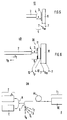
- the basic principle of the optical reflection modulator is shown in FIG. In the following, the optical reflection modulator is simply called the modulator for the sake of simplicity.
- the modulator 1 has the following parts: an end face of a optical waveguide 2 through which light emerges. This end surface is called second mirror surface 4 below.
- a first mirror surface 3 is arranged opposite it.
- the mirror surfaces 3 and 4 lie parallel to one another and thus form a Fabry-Perot resonator 5 with a resonator length x between the two mirror surfaces 3 and 4.
- the resonator length x is an optical length, ie the refractive index of a medium contained in the Fabry-Perot resonator 5 is taken into account.
- the variation of the resonator length x only represents a special type of detuning of the Fabry-Perot resonator 5.
- the resonator 5 can also be tilted out by one of the two Mirror surfaces 3, 4 out of their plane, or by deforming one of the two mirror surfaces 3, 4, or in another way or in combination of the above-mentioned possibilities.
- the implementation of a modulator using some of the aforementioned detuning options is shown below in the exemplary embodiments.
- the resonator 5 can contain imaging optics in the beam path between the two mirror surfaces 3 and 4.
- a glass fiber optical waveguide is advantageously used as the optical waveguide 2.
- the second mirror surface 4 is an end surface of the glass fiber optical waveguide, which is preferably at right angles to the glass fiber cladding.
- the quality of the resonator 5 can be adjusted by changing the reflectance of the mirror surfaces 3, 4 in a known manner, for example by applying selected layers.
- the modulator 20 has a thickness oscillator 8 in the form of a piezoelectric transducer with electrical connections 7, to which a modulation voltage U m , ie the modulation signal, can be applied.
- the first mirror surface 3 is connected to the piezoelectric transducer 8 in such a way that the resonator length x changes when the modulation voltage U m is applied .
- FIG. 4 shows the second exemplary embodiment of a modular gate 30, in which the detuning is likewise carried out by varying the resonator length x.
- a birefringent medium 9 is arranged between two electrodes E, to which the modulation voltage U m is applied, the refractive index n of which can be changed by applying the modulation voltage U m .
- the resonator length x changes due to the change in the refractive index of the medium 9.
- the first mirror surface 3 lies on a surface of the medium 9 which is at right angles to the surfaces on which the electrodes E bear.
- the second mirror surface 4 is located on the side of the medium 9 that lies opposite the first mirror surface 3.
- the third exemplary embodiment of a modular gate 10 is shown in FIG. 5.
- this modulator 10 only the thickness transducer 8 is replaced by a flexural transducer 6, preferably a quartz oscillator, compared to the modulator 20 from FIG. 3.
- the Fabry-Perot resonator 5 is detuned by a combination of the variation in the resonator length x and the tilting of the first mirror surface 3 out of its rest plane.
- FIG. 6 shows a transmission and reception module 40, which is provided with a modulator according to the invention, here the modulator 20 of the second exemplary embodiment.
- a modulator according to the invention, here the modulator 20 of the second exemplary embodiment.
- a signal diode for example a PIN photodiode, is arranged on the thickness transducer 8 for message signals.
- the first mirror surface 3 forms the entry surface of the light into the photodiode 11.
- the generated photocurrent I P flows through the connections 12.
- the photodiode 11 detects the incident light with the power P T minus the reflected portion. Since the generated photocurrent I P depends only slightly on the resonator length x, there is no disturbing modulation of the photocurrent I P by varying the resonator length x. A typical value of the disturbance is less than 1 dB.
- a particular advantage of the modulator 10, 20, 30 over the known modulator lies in the uncomplicated coupling between the optical waveguide 2 and the Fabry-Perot resonator 5.
- the modulators 10, 20, 30 only require coupling with the quality of an average waveguide -Photodiode coupling, whereas for the known modulator, due to its "integrated optical waveguide", a coupling with the higher quality of a waveguide-laser coupling is necessary.
- the arrangement of a bending oscillator 6 in a transmitting and receiving module 40 reduces the coupling problem compared to the known transmitting and receiving module at least in the direction of adjustment, which lies in the direction of movement of the bending oscillator 6.
- the complete mode of operation of the transmitting and receiving module is explained using an exemplary embodiment of an optical message transmission system ON.
- the reflected and modulated with the frequency f 1 signal is now transmitted via the same optical waveguide AL and the star distributor S to the central station Z and is fed there via an 3dB power coupler K to an optical receiver module E. This is followed by an electrical receiver that filters and demodulates the desired band, for example with the modulation frequency f 1.
- the operating point is preferably from one of the antinodes of the standing wave by the distance ⁇ 0 / 8.
- NRZ Network Return to Zero
- These signals can be amplitude, phase or frequency modulated.
- the optical message transmission system ON enables a single laser module L located in the center Z to supply a plurality of subscribers T i via the star distributor S, which in turn can transmit signals directed to the center Z by modulating the received carrier.
- the identification of the individual subscriber signals in the central Z is carried out by using different frequencies f 1 of the subcarrier.
- the transmission in the downward direction is broadband in the exemplary embodiment, e.g. for cable television and telephony; the transmission in the upward direction is narrowband, e.g. for telephony only.
- symmetrical broadband transmission is also possible, in particular when using the modulator 30 of the second exemplary embodiment.
Description
Die Erfindung betrifft ein optisches Sende- und Empfangsmodul, ein Verfahren zur Modulation des Moduls und ein optisches Übertragungssystem mit solchen Modulen.The invention relates to an optical transmission and reception module, a method for modulating the module and an optical transmission system with such modules.
Derartige Modulatoren finden ihre Anwendung in optischen Nachrichtenübertragungssystemen, bei denen eine Leitungsendeinrichtung, ohne eine Lichtquelle zu enthalten, das zu sendende Signal erzeugt. Der optische Träger für ein solches Sendesignal wird bei diesen Systemen in einer Zentrale erzeugt und über einen optischen Wellenleiter der Leitungsendeinrichtung zugeführt, dort moduliert, und das entstehende Sendesignal wird vorzugsweise über denselben optischen Wellenleiter übertragen.Such modulators are used in optical communication systems in which a line terminal device, without containing a light source, generates the signal to be transmitted. In these systems, the optical carrier for such a transmission signal is generated in a center and fed to the line end device via an optical waveguide, modulated there, and the resulting transmission signal is preferably transmitted via the same optical waveguide.
Aus der Druckschrift Electronics Letters 8th May, Vol. 22, No. 10, Seiten 517 bis 518 ist ein System mit einem Reflexionsmodulator beschrieben. Der beschriebene Reflexionsmodulator besteht aus einem elektrooptisch aktiven Wellenleiterkoppler, der als Schalter betreibbar und in einer integrierten optischen Schaltung enthalten ist.From the publication Electronics Letters 8th May, Vol. 22, No. 10, pages 517 to 518, a system with a reflection modulator is described. The described reflection modulator consists of an electro-optically active waveguide coupler which can be operated as a switch and is contained in an integrated optical circuit.
Er hat zwei Zweige mit je zwei Anschlüssen. Der optische Wellenleiter zur Nachrichtenübertragung ist an einem ersten Anschluß des ersten Zweiges und die Spiegelfläche an einem ersten Anschluß des zweiten Zweiges angeordnet. Durch geeignetes Schalten kann aus dem optischen Wellenleiter in den Modulator eintretendes Licht über die Spiegelfläche in den optischen Wellenleiter zurückreflektiert werden. Betrachtet man das in den Modulator eintretende Licht als einen optischen Träger und das Schalten als Modulation, so läßt sich sagen, daß durch Modulation des Trägers ein optisches Sendesignal erzeugt wird.It has two branches with two connections each. The optical waveguide for message transmission is on a first one Connection of the first branch and the mirror surface arranged on a first connection of the second branch. By suitable switching, light entering the modulator from the optical waveguide can be reflected back into the optical waveguide via the mirror surface. If one considers the light entering the modulator as an optical carrier and the switching as modulation, it can be said that an optical transmission signal is generated by modulating the carrier.
Der Nachteil des bekannten optischen Reflexionsmodulators liegt nun darin, daß die Justierung zwischen optischen Wellenleiter und der integrierten optischen Schaltung, in der sich der Reflexionsmodulator befindet, sehr genau sein muß und technologisch entsprechend aufwendig ist.The disadvantage of the known optical reflection modulator is that the adjustment between the optical waveguide and the integrated optical circuit in which the reflection modulator is located must be very precise and is technologically correspondingly complex.
Der Erfindung liegt die Aufgabe zugrunde, einen optischen Reflexionswellenleiter zu schaffen, bei dem dieser Nachteil beseitigt ist.The invention has for its object to provide an optical reflection waveguide in which this disadvantage is eliminated.
Die Aufgabe wird durch die Merkmale des Anspruches 1 gelöst.The object is achieved by the features of
Weitere Ausgestaltungen der Erfindung sind den übrigen Ansprüchen und dem Rest der Beschreibung zu entnehmen.Further refinements of the invention can be found in the remaining claims and the rest of the description.
Ein besonderer Vorteil der Erfindung liegt in der Verwendung des Reflexionsmodulators in einem Sende- und Empfangsmodul. Vorteilhaft ist, daß kein Koppler zur Aufteilung der Trägerleistung zum Teil für die Photodiode und zum Teil für die Spiegelfläche notwendig ist, und daß in dem Sende- und Empfangsmodul, in der Betriebsweise als Sendemodul, dem Sendesignal keine störenden Reflexe von der Oberfläche der Photodiode zugemischt werden.A particular advantage of the invention lies in the use of the reflection modulator in a transmission and reception module. It is advantageous that no coupler for dividing the carrier power is partly necessary for the photodiode and partly for the mirror surface, and that in the transmitting and receiving module, in the mode of operation as a transmitting module, no disturbing reflections from the surface of the photodiode are added to the transmitted signal become.
Ein weiterer Vorteil der Erfindung liegt darin, daß die benötigten Komponenten als Serienprodukte auf dem Markt erhältlich sind.Another advantage of the invention is that the required components are available on the market as series products.
Fünf Ausführungsbeispiele der Erfindung werden anhand von sieben Figuren beschrieben. Es zeigen:
- Fig. 1
- das Grundprinzip des optischen Reflexionsmodulators,
- Fig. 2
- den relativen Pegel der in die Faser zurückreflektierten Leistung über der Resonatorlänge x aufgetragen,
- Fig. 3
- ein erstes Ausführungsbeispiel eines optischen Reflexionsmodulators mit einem Dickenschwinger als Schwingelement,
- Fig. 4
- ein zweites Ausführungsbeispiel eines optischen Reflexionsmodulators mit einem elektrooptisch aktiven Medium zur Variation der Resonatorlänge x,
- Fig. 5
- ein drittes Ausführungsbeispiel eines optischen Reflexionsmodulators mit einem Biegeschwinger als Schwingelement,
- Fig. 6
- ein Ausführungsbeispiel eines erfindungsgemäße Sende- und Empfangsmoduls, und
- Fig. 7
- ein Ausführungsbeispiel eines erfindungsgemäße optischen Übertragungssystems.
- Fig. 1
- the basic principle of the optical reflection modulator,
- Fig. 2
- plotted the relative level of the power reflected back into the fiber over the resonator length x,
- Fig. 3
- a first embodiment of an optical reflection modulator with a thickness transducer as a vibrating element,
- Fig. 4
- a second embodiment of an optical reflection modulator with an electro-optically active medium for varying the resonator length x,
- Fig. 5
- A third embodiment of an optical reflection modulator with a bending oscillator as a vibrating element,
- Fig. 6
- an embodiment of a transmission and reception module according to the invention, and
- Fig. 7
- an embodiment of an optical transmission system according to the invention.
In Fig. 1 ist das Grundprinzip des optischen Reflexionsmodulators abgebildet. Im folgenden wird der optische Reflexionsmodulator einfachheitshalber nur Modulator genannt. Der Modulator 1 weist folgende Teile auf: Eine Endfläche eines optischen Wellenleiters 2, durch die Licht austritt. Diese Endfläche wird im folgenden zweite Spiegelfläche 4 genannt. Ihr gegenüberliegend ist eine erste Spiegelfläche 3 angeordnet. Die Spiegelflächen 3 und 4 liegen parallel zueinander und bilden so einen Fabry-Perot Resonator 5 mit einer Resonatorlänge x zwischen den beiden Spiegelflächen 3 und 4. Die Resonatorlänge x ist eine optische Länge, d.h. der Brechungsindex eines im Fabry-Perot-Resonator 5 enthaltenen Mediums ist berücksichtigt.The basic principle of the optical reflection modulator is shown in FIG. In the following, the optical reflection modulator is simply called the modulator for the sake of simplicity. The
Durch die zweite Spiegelfläche 4 wird Licht mit dem Leistungspegel PT in den Fabry-Perot Resonator 5 eingekoppelt und an der ersten Spiegelfläche 3 wenigstens teilweise reflektiert und somit teilweise wieder über die zweite Spiegelfläche 4 in den optischen Wellenleiter 2 zurückgekoppelt. Im Fabry-Perot Resonator 5 bildet sich dabei eine stehende Welle. Der typische Verlauf des in den optischen Wellenleiter 2 reflektierten Anteils des Lichts mit dem Leistungspegel PR, bezogen auf den Leistungspegel PT des eintretenden Lichts, ist in Fig. 2 über der Resonatorlänge x aufgetragen. Es ist zu erkennen, daß der relative Leistungspegel PR/PT zwischen einem minimalen Leistungspegel P₁, der kleiner als -40 dB ist, und einem maximalen Leistungspegel P₂ bei -8 dB periodisch schwankt. Der periodische Abstand x₀ ist die halbe Wellenlänge des Lichts, was bei einer Wellenlänge von z.B. λ₀ = 1300 nm einem Wert x₀ = 650 nm entspricht. Durch Variation der Resonatorlänge x kann somit der Leistungspegel PR des in den optischen Wellenleiter 2 zurückreflektierten Lichtanteils verändert und somit der optische Träger amplitudenmoduliert werden. Diese Variation wird im folgenden als Modulationshub bezeichnet.Through the
Die Variation der Resonatorlänge x stellt dabei lediglich eine spezielle Art einer Verstimmung des Fabry-Perot Resonators 5 dar. Der Resonator 5 kann auch durch Herauskippen einer der beiden Spiegelflächen 3, 4 aus ihrer Ebene, oder durch Verformen einer der beiden Spiegelflächen 3, 4, oder auf andere Weise oder in Kombination der oben genannten Möglichkeiten verstimmt werden. Die Realisierung eines Modulators unter Ausnützung einiger genannter Verstimmöglichkeiten wird nachstehend in den Ausführungsbeispielen gezeigt.The variation of the resonator length x only represents a special type of detuning of the Fabry-Perot
Um Divergenzverluste der Lichtleistung beim Austreten des Lichtes aus dem optischen Wellenleiter 2 zu reduzieren, kann der Resonator 5 im Strahlengang zwischen den beiden Spiegelflächen 3 und 4 eine Abbildungsoptik enthalten.In order to reduce divergence losses in the light output when the light emerges from the
Aufgrund der Divergenz des aus dem optischen Wellenleiter 2 austretenden Lichts ist es nicht zwangsläufig notwendig, als Resonator einen Fabry-Perot Resonator 5 mit zwei parallel liegenden Spiegelflächen 3 und 4 anzuordnen. Wenn die Flächennormalen der beiden Spiegelflächen 3 und 4 einen Winkel einschließen, der sich von null Grad unterscheidet, wird auf diese Weise aus dem optischen Wellenleiter 2 gebeugt austretendes Licht über die erste Spiegelfläche 3 zum optischen Wellenleiter 2 zurückreflektiert. Wird der, von den Flächennormalen der beiden Spiegelflächen 3 und 4, eingeschlossene Winkel in Ruhestellung ungleich null Grad gewählt, empfiehlt es sich, den Reflexionsgrad der ersten Spiegelfläche 3 mit zunehmendem Winkel kleiner zu wählen.Because of the divergence of the light emerging from the
Als optischer Wellenleiter 2 wird vorteilhafterweise ein Glasfaser-Lichtwellenleiter verwendet. Die zweite Spiegelfläche 4 ist dabei eine Endfläche des Glasfaser-Lichtwellenleiters, die vorzugsweise im rechten Winkel zum Glasfasermantel steht.A glass fiber optical waveguide is advantageously used as the
Die Güte des Resonators 5 kann dadurch eingestellt werden, daß der Reflexionsgrad der Spiegelflächen 3, 4 in bekannter Weise verändert wird, z.B. indem ausgewählte Schichten aufgebracht werden.The quality of the
In Fig. 3 ist ein erstes Ausführungsbeispiel eines Modulators 20 abgebildet. Der Modulator 20 weist zusätzlich zu den schon in Fig. 1 abgebildeten und oben beschrieben Merkmalen als mechanische Schwingvorrichtung einen Dickenschwinger 8 in Form eines piezoelektrischen Wandlers mit elektrischen Anschlüssen 7 auf, an denen eine Modulationsspannung Um, d.h. das Modulationssignal angelegt werden kann. Die erste Spiegelfläche 3 ist derart mit dem piezoelektrischen Wandler 8 verbunden, daß sich die Resonatorlänge x durch Anlegen der Modualtionsspannung Um verändert.3 shows a first exemplary embodiment of a
In Fig. 4 ist das zweite Ausführungsbeispiel eines Modualtors 30 abgebildet, bei dem die Verstimmung ebenfalls durch Variation der Resonatorlänge x erfolgt. Hierzu ist zwischen zwei Elektroden E, an denen die Modulationsspannung Um angelegt wird, ein doppelbrechendes Medium 9 angeordnet, dessen Brechungsindex n durch Anlegen der Modulationsspannung Um veränderbar ist. Durch die Veränderung des Brechungsindexes des Mediums 9 ändert sich die Resonatorlänge x. Die erste Spiegelfläche 3 liegt auf einer Fläche des Mediums 9, die zu den Flächen, an denen die Elektroden E anliegen, rechtwinklig steht. Die zweite Spiegelfläche 4 befindet sich auf der Seite des Mediums 9, die der ersten Spiegelfläche 3 gegenüberliegt.4 shows the second exemplary embodiment of a
Das dritte Ausführungsbeispiel eines Modualtors 10 ist in Fig. 5 abgebildet. Bei diesem Modulator 10 ist gegenüber dem Modulator 20 aus Fig. 3 lediglich der Dickenschwinger 8 durch einen Biegeschwinger 6, vorzugsweise durch einen Schwingquarz, ersetzt. Die Verstimmung des Fabry-Perot Resonators 5 erfolgt bei diesem Modulator 10 durch eine Kombination der Variation der Resonatorlänge x und des Herauskippens der ersten Spiegelfläche 3 aus ihrer Ruheebene.The third exemplary embodiment of a
In Fig. 6 ist ein Sende- und Empfangsmodul 40 abgebildet, das mit einem erfindungsgemäßen Modulator, hier dem Modulator 20 des zweiten Ausführungsbeispiels, versehen ist. Zum Empfang von Nachrichtensignalen ist eine Photodiode 11, z.B. eine PIN-Photodiode, auf dem Dickenschwinger 8 angeordnet. Die erste Spiegelfläche 3 bildet dabei die Eintrittsfläche des Lichts in die Photodiode 11. Der erzeugte Photostrom IP fließt über die Anschlüsse 12.6 shows a transmission and
Die Photodiode 11 detektiert das mit der Leistung PT einfallende Licht abzüglich des reflektierten Anteils. Da der erzeugte Photostrom IP nur geringfügig von der Resonatorlänge x abhängt, erfolgt keine störende Modulation des Photostroms IP durch die Variation der Resonatorlänge x. Ein typischer Wert der Störung liegt unter 1 dB.The photodiode 11 detects the incident light with the power P T minus the reflected portion. Since the generated photocurrent I P depends only slightly on the resonator length x, there is no disturbing modulation of the photocurrent I P by varying the resonator length x. A typical value of the disturbance is less than 1 dB.
Ein besonderer Vorteil des Modulators 10, 20, 30 gegenüber dem bekannten Modulator liegt in der unkomplizierten Ankopplung zwischen dem optischen Wellenleiter 2 und dem Fabry-Perot-Resonator 5. Die Modulatoren 10, 20, 30 erfordern lediglich eine Ankopplung mit der Qualität einer durchschnittlichen Wellenleiter-Photodioden-Kopplung, wohingegen für den bekannten Modulator, aufgrund seiner "integrierten optischen Wellenleiter", eine Ankopplung mit der höheren Qualität einer Wellenleiter-Laser-Kopplung notwendig ist.A particular advantage of the
Die Anordnung eines Biegeschwingers 6 in einem Sende- und Empfangsmodul 40 reduziert das Ankopplungsproblem gegenüber dem bekannten Sende- und Empfangsmodul wenigstens in der Justierrichtung, die in der Bewegungsrichtung des Biegeschwingers 6 liegt.The arrangement of a bending
Die vollständige Funktionsweise des Sende- und Empfangsmoduls wird an einem Ausführungsbeispiel eines optischen Nachrichtenübertragungssystems ON erläutert. Zu dem Nachrichtenübertragungssystem ON gehört eine Zentrale Z und mehrere Teilnehmer Ti mit i = 1, 2, ..., N. Beispielhaft wird nur die Übertragung von der Zentrale Z zu einem Teilnehmer T₁ und zurück beschrieben. Die Zentrale Z enthält ein Lasermodul L, das einen mit einer Frequenz f₀ = 5 MHz modulierten Träger mit einer Wellenlänge von λ₀ = 1300 nm erzeugt. Dieser modulierte Träger wird über einen Sternverteiler S und einen optischen Wellenleiter AL zu einem Sende- und Empfangsmodul SE beim Teilnehmer T₁ übertragen und dort empfangen. Im Sende- und Empfangsmodul SE wird das Licht durch den optischen Reflexionsmodulator mit einer Modulationsfrequenz f₁ = 600 kHz moduliert. Es ist dabei zu beachten, daß sich die Modulationsbänder einschließlich der Seitenbänder und der Harmonischen nicht überlagern. Das reflektierte und mit der Frequenz f₁ modulierte Signal wird nun über denselben optischen Wellenleiter AL und den Sternverteiler S zur Zentrale Z übertragen und dort über einen 3dB-Leistungskoppler K einem optischen Empfängermodul E zugeführt. Diesem ist ein elektrischer Empfänger nachgeschaltet, der das gewünschte Band, z.B. mit der Modulationsfrequenz f₁, ausfiltert und demoduliert.The complete mode of operation of the transmitting and receiving module is explained using an exemplary embodiment of an optical message transmission system ON. A center Z and belongs to the message transmission system ON several subscribers T i with i = 1, 2, ..., N. As an example, only the transmission from the central station Z to a
Erfolgt die Modulation im Sende- und Empfangsmodul SE durch eine Schwingung der ersten Spiegelfläche 3 über mehrere Schwingungsknoten der stehenden Welle im Fabry-Perot-Resonator 5, werden aufgrund von Nichtlinearitäten auch Störmodulationen mit einem Bandabstand von jeweils der Modulationsfrequenz f₁ = 600 kHz erzeugt. Diese Störmodulationen können im Empfangsmodul E in oben beschriebener Weise elektrisch ausgefiltert werden.If the modulation in the transmission and reception module SE is carried out by an oscillation of the
Zur Übertragung vom Sende- und Empfangsmodul SE des Trägers 1 E₁ zur Zentrale Z im Basisband ist es notwendig, den Modualtionshub im optischen Reflexionsmodulator auf einen Wert von etwa λ₀/4 zu begrenzen. Der Arbeitspunkt liegt vorzugsweise von einem der Schwingungsbäuche der stehenden Welle um die Strecke λ₀/8 entfernt.To transmit from the transmission and reception module SE of the carrier 1
Die Übertragung von der Zentrale Z zu den Teilnehmern, wie auch in entgegengesetzter Richtung erfolgt über Signale, die mit einem NRZ (None Return to Zero)-Code codiert sind. Diese Signale können amplituden-, phasen- oder frequenzmoduliert sein.The transmission from the central office Z to the subscribers, as well as in the opposite direction, takes place via signals which are coded with an NRZ (None Return to Zero) code. These signals can be amplitude, phase or frequency modulated.
Das optische Nachrichtenübertragungssystem ON ermöglicht es, daß mit einem einzigen, sich in der Zentrale Z befindlichen Lasermodul L über den Sternverteiler S mehrere Teilnehmer Ti versorgt werden können, die ihrerseits an die Zentrale Z gerichtete Signale durch Modulation des empfangenen Trägers übertragen können. Die Identifikation der einzelnen Teilnehmersignale in der Zentrale Z erfolgt durch die Verwendung unterschiedlicher Frequenzen f₁ des Unterträgers.The optical message transmission system ON enables a single laser module L located in the center Z to supply a plurality of subscribers T i via the star distributor S, which in turn can transmit signals directed to the center Z by modulating the received carrier. The identification of the individual subscriber signals in the central Z is carried out by using
Die Übertragung in Abwärtsrichtung erfolgt im Ausführungsbeispiel breitbandig, z.B. für Kabelfernsehen und Fernsprechen; die Übertragung in Aufwärtsrichtung erfolgt schmalbandig, z.B. nur für Fernsprechen. Es ist aber insbesondere bei der Verwendung des Modulators 30 des zweiten Ausführungsbeispiels auch eine symmetrische Breitbandübertragung möglich.The transmission in the downward direction is broadband in the exemplary embodiment, e.g. for cable television and telephony; the transmission in the upward direction is narrowband, e.g. for telephony only. However, symmetrical broadband transmission is also possible, in particular when using the
Claims (11)
- Optical transceiver module including an optical waveguide (2), a modulation device and a photodiode (11),- wherein the modulation device comprises a detunable optical resonator (5) having a first and a second reflective surface (3, 4) arranged opposite one another and the second reflective surface (4) represents the end face of the optical waveguide (2),- wherein, following the pass through the resonator (5), light exiting from the end face of the optical waveguide (2) is detectable as a received signal in a photodiode (11) arranged behind the first reflective surface (3), and- wherein the light disposed in the resonator (5) can be coupled back via the second reflective surface (4) into the optical waveguide (2) and can be modulated as a carrier with a modulation signal by detuning the resonator (5).
- Optical transceiver module according to claim 1, characterized in that, in the quiescent state, the normals of the first and second reflective surfaces (3, 4) are parallel, that is, the resonator (5) is a Fabry-Perot resonator (5).
- Optical transceiver module according to claim 1, characterized in that the normals of the first and second reflective surfaces (3, 4) are not parallel in the quiescent state.
- Optical transceiver module according to one of claims 1 to 3, characterized in that the optical length of the resonator can be varied in a controlled manner by the modulation signal.
- Optical transceiver module according to claim 4, characterized in that a birefringent medium (9) having a variable refractive index is disposed between the reflective surfaces (3, 4) in order to vary the optical length.
- Optical transceiver module according to one of claims 1 to 5, characterized in that at least one of the two reflective surfaces (3, 4) is arranged to be movable through an angle under control of the modulation signal.
- Optical transceiver module according to one of claims 1 to 6, characterized in that, in order to detune the resonator, the first reflective surface (3) is disposed on a mechanical vibrator device (6, 8) which can be actuated by the modulation signal.
- Optical transceiver module according to claim 1, characterized in that the first reflective surface (3) is the surface through which the light enters the photodiode (11).
- Method for the modulation of an optical transceiver module according to one of claims 1 to 8, characterized in that the modulation of the carrier is effected with a modulation deviation of the resonator length (x), the deviation being larger than half of the wavelength (λ₀) of the carrier.
- Method for the modulation of light by means of an optical transceiver module according to one of claims 1 to 7, characterized in that the modulation is effected by varying the resonator length (x) with a modulation deviation which is smaller than one quarter of the wavelength λ₀ of the light and the operating point is removed from one of the oscillation antinodes of the standing wave of a distance λ₀/8.
- Optical transmission system having a central station and several subscribers, wherein the subscribers are provided with optical transceiver modules according to one of claims 1 to 8 for the generation of a transmission signal, wherein the carrier of the optical transmission signal of several subscribers can be generated in a laser module of the central station and this carrier can be modulated at the individual subscribers, with it being possible to provide the carrier at the individual subscribers (Ti, i = 1, 2, ... N) with a subcarrier and the frequency of the subcarriers of the individual subscribers (Ti, i = 1, 2, ... N) being different.
Applications Claiming Priority (2)
| Application Number | Priority Date | Filing Date | Title |
|---|---|---|---|
| DE4031970 | 1990-10-09 | ||
| DE4031970A DE4031970A1 (en) | 1990-10-09 | 1990-10-09 | OPTICAL REFLECTION MODULATOR |
Publications (3)
| Publication Number | Publication Date |
|---|---|
| EP0480231A2 EP0480231A2 (en) | 1992-04-15 |
| EP0480231A3 EP0480231A3 (en) | 1992-06-10 |
| EP0480231B1 true EP0480231B1 (en) | 1995-12-27 |
Family
ID=6415910
Family Applications (1)
| Application Number | Title | Priority Date | Filing Date |
|---|---|---|---|
| EP91116202A Expired - Lifetime EP0480231B1 (en) | 1990-10-09 | 1991-09-24 | Optical emitter-receiver module |
Country Status (6)
| Country | Link |
|---|---|
| US (1) | US5253099A (en) |
| EP (1) | EP0480231B1 (en) |
| JP (1) | JPH04263212A (en) |
| CA (1) | CA2053022C (en) |
| DE (2) | DE4031970A1 (en) |
| ES (1) | ES2084077T3 (en) |
Families Citing this family (18)
| Publication number | Priority date | Publication date | Assignee | Title |
|---|---|---|---|---|
| US6693736B1 (en) | 1992-09-10 | 2004-02-17 | Fujitsu Limited | Optical circuit system and components of same |
| EP0617314A4 (en) | 1992-09-10 | 1995-10-18 | Fujitsu Ltd | Optical circuit system and its constituents. |
| DE59309409D1 (en) * | 1992-11-20 | 1999-04-08 | Ascom Tech Ag | Light modulator |
| EP0599154A1 (en) * | 1992-11-20 | 1994-06-01 | Ascom Tech Ag | Lightbeam-modulator |
| EP0729051A3 (en) * | 1995-02-21 | 1998-06-17 | Ascom Tech Ag | Optical reflection modulator |
| US5796880A (en) * | 1996-11-18 | 1998-08-18 | Lucent Technologies Inc. | Technique for modulating optical signals in optical communications |
| WO2004066460A1 (en) * | 2003-01-23 | 2004-08-05 | Nlg - New Laser Generation Gmbh | Laser resonator and frequency-converted laser |
| GB2399921B (en) * | 2003-03-26 | 2005-12-28 | Schlumberger Holdings | Borehole telemetry system |
| GB2418028B (en) * | 2003-05-07 | 2007-08-01 | Qinetiq Ltd | Dynamic optical reflector and interrogation system |
| US7606537B2 (en) * | 2004-02-10 | 2009-10-20 | Colin Dugald Brodhead | System and method for transmitting data via wave reflection |
| JP5017765B2 (en) * | 2004-03-30 | 2012-09-05 | 日本電気株式会社 | OPTICAL MODULATOR, MANUFACTURING METHOD THEREOF, MODULATION OPTICAL SYSTEM, OPTICAL INTERCONNECT DEVICE USING SAME, AND OPTICAL COMMUNICATION DEVICE |
| US7348893B2 (en) * | 2004-12-22 | 2008-03-25 | Schlumberger Technology Corporation | Borehole communication and measurement system |
| GB0515523D0 (en) * | 2005-07-28 | 2005-12-07 | Bae Systems Plc | Transponder |
| GB0521253D0 (en) * | 2005-10-19 | 2005-11-30 | Qinetiq Ltd | Optical angle detection |
| US8224189B1 (en) | 2007-02-02 | 2012-07-17 | Sunlight Photonics Inc. | Retro-directive target for free-space optical communication and method of producing the same |
| US8204384B2 (en) * | 2008-11-21 | 2012-06-19 | Cubic Corporation | Phase-modulating communication device |
| US8498502B2 (en) | 2010-12-17 | 2013-07-30 | Fujitsu Limited | Device for phase modulation |
| US11018778B1 (en) * | 2020-05-20 | 2021-05-25 | Verizon Patent And Licensing Inc. | System and method to prevent unauthorized voice detection via fiber links |
Family Cites Families (11)
| Publication number | Priority date | Publication date | Assignee | Title |
|---|---|---|---|---|
| US4209689A (en) * | 1969-06-04 | 1980-06-24 | Hughes Aircraft Company | Laser secure communications system |
| US3863064A (en) * | 1972-01-03 | 1975-01-28 | Philco Ford Corp | Differential retrocommunicator |
| US4446543A (en) * | 1979-07-02 | 1984-05-01 | The United States Of America As Represented By The Secretary Of The Navy | Optical resonator single-mode fiber hydrophone |
| US4268116A (en) * | 1979-10-26 | 1981-05-19 | Optelecom Incorporated | Method and apparatus for radiant energy modulation in optical fibers |
| US4358851A (en) * | 1980-02-28 | 1982-11-09 | Xerox Corporation | Fiber optic laser device and light emitter utilizing the device |
| US4577924A (en) * | 1982-06-03 | 1986-03-25 | General Dynamics Electronics Division | Optical recursive filter |
| US4744625A (en) * | 1982-09-30 | 1988-05-17 | Gte Laboratories Incorporated | Methods of and apparatus for providing frequency modulated light |
| US4533829A (en) * | 1983-07-07 | 1985-08-06 | The United States Of America As Represented By The Secretary Of The Air Force | Optical electromagnetic radiation detector |
| US4937833A (en) * | 1985-03-25 | 1990-06-26 | The United States Of America As Represented By The Secretary Of The Navy | Analog frequency modulated laser using magnetostriction |
| FR2585849B1 (en) * | 1985-07-30 | 1988-12-30 | Suisse Electro Microtech Centr | FIBER OPTIC SENSING SYSTEM INCORPORATING AN INTENSITY MODULATED SENSOR |
| GB2190789B (en) * | 1986-04-17 | 1990-05-09 | Plessey Co Plc | System for optically coupling components of integrated circuits |
-
1990
- 1990-10-09 DE DE4031970A patent/DE4031970A1/en not_active Withdrawn
-
1991
- 1991-09-16 US US07/760,469 patent/US5253099A/en not_active Expired - Fee Related
- 1991-09-24 EP EP91116202A patent/EP0480231B1/en not_active Expired - Lifetime
- 1991-09-24 ES ES91116202T patent/ES2084077T3/en not_active Expired - Lifetime
- 1991-09-24 DE DE59107145T patent/DE59107145D1/en not_active Expired - Fee Related
- 1991-09-30 JP JP3278668A patent/JPH04263212A/en active Pending
- 1991-10-08 CA CA002053022A patent/CA2053022C/en not_active Expired - Fee Related
Also Published As
| Publication number | Publication date |
|---|---|
| EP0480231A2 (en) | 1992-04-15 |
| CA2053022C (en) | 1998-11-24 |
| JPH04263212A (en) | 1992-09-18 |
| EP0480231A3 (en) | 1992-06-10 |
| US5253099A (en) | 1993-10-12 |
| DE59107145D1 (en) | 1996-02-08 |
| ES2084077T3 (en) | 1996-05-01 |
| CA2053022A1 (en) | 1992-04-10 |
| DE4031970A1 (en) | 1992-04-16 |
Similar Documents
| Publication | Publication Date | Title |
|---|---|---|
| EP0480231B1 (en) | Optical emitter-receiver module | |
| DE3232430C2 (en) | Optical communication system | |
| DE60222889T2 (en) | WAVE LENGTH CONTROL WITH DITHER MODULATION AND FEEDBACK | |
| DE3501967C2 (en) | Optical data connection | |
| EP0383138A2 (en) | Device for the direct optical reception of a plurality of wave lengths | |
| DE4415176A1 (en) | Device and method for dispersion compensation in a fiber optic transmission system | |
| EP0096327A1 (en) | Distribution network | |
| EP0354567A2 (en) | Sending and receiving part for a bidirectional coherent optical communication system | |
| EP0883259A2 (en) | CDMA receiver for an optical transmission system and a method of operating this receiver | |
| DE3637809A1 (en) | TRANSMITTER FOR COHERENT WAVES | |
| EP0644668B1 (en) | Transmitting and receiving module for bidirectional optical multichannel transmission | |
| DE60308244T2 (en) | Method and device for producing a suppressed carrier optical pulse train and grating device | |
| EP0361151A2 (en) | Device for generating an FSK-modulated optical signal with two different polarisation states for an optical transmission system with an optical heterodyne FSK receiver having two filters | |
| EP0320688B1 (en) | Retroreflective transceiver for a bidirectional fibre-optical communication system | |
| US5526159A (en) | Method and circuit arrangement for electric compensation of signal distortion caused by laser chirp and fiber dispersion | |
| EP1378074B1 (en) | Device and system for the optical transmission of data between satellites | |
| DE60200221T2 (en) | Optical transmitter, system and method for transmitting signals with high data rates | |
| EP0359967A2 (en) | External optical resonator for a semiconductor laser | |
| DE60201200T2 (en) | Optical Pulse Source for Remote Optical Transmission Systems | |
| DE60030446T2 (en) | System and device for sending optical data | |
| EP0717514A2 (en) | Optical transmission device for an optical telecommunication system in combination with a radio system | |
| EP0301388B1 (en) | Reflective transmitter for a fibre-optical bidirectional communication system | |
| DE4223175A1 (en) | Integrated optical bidirectional Y=shaped injection laser termination for data communication - has photodetector and reflection modulator in respective branches of Y, and couples to external optical path at opposite end of Y | |
| EP0142020A2 (en) | Optical transmission line | |
| EP0509500A2 (en) | Device for bidirectional simultaneous transmission of digital information |
Legal Events
| Date | Code | Title | Description |
|---|---|---|---|
| PUAI | Public reference made under article 153(3) epc to a published international application that has entered the european phase |
Free format text: ORIGINAL CODE: 0009012 |
|
| AK | Designated contracting states |
Kind code of ref document: A2 Designated state(s): BE CH DE ES FR GB IT LI NL |
|
| PUAL | Search report despatched |
Free format text: ORIGINAL CODE: 0009013 |
|
| AK | Designated contracting states |
Kind code of ref document: A3 Designated state(s): BE CH DE ES FR GB IT LI NL |
|
| 17P | Request for examination filed |
Effective date: 19920520 |
|
| RAP3 | Party data changed (applicant data changed or rights of an application transferred) |
Owner name: ALCATEL N.V. Owner name: ALCATEL SEL AKTIENGESELLSCHAFT |
|
| 17Q | First examination report despatched |
Effective date: 19931130 |
|
| GRAA | (expected) grant |
Free format text: ORIGINAL CODE: 0009210 |
|
| AK | Designated contracting states |
Kind code of ref document: B1 Designated state(s): BE CH DE ES FR GB IT LI NL |
|
| REF | Corresponds to: |
Ref document number: 59107145 Country of ref document: DE Date of ref document: 19960208 |
|
| REG | Reference to a national code |
Ref country code: CH Ref legal event code: NV Representative=s name: JUERG ULRICH C/O ALCATEL STR AG |
|
| ITF | It: translation for a ep patent filed |
Owner name: DOTT. ANTONIO SERGI |
|
| GBT | Gb: translation of ep patent filed (gb section 77(6)(a)/1977) |
Effective date: 19960222 |
|
| ET | Fr: translation filed | ||
| REG | Reference to a national code |
Ref country code: ES Ref legal event code: FG2A Ref document number: 2084077 Country of ref document: ES Kind code of ref document: T3 |
|
| PLBE | No opposition filed within time limit |
Free format text: ORIGINAL CODE: 0009261 |
|
| STAA | Information on the status of an ep patent application or granted ep patent |
Free format text: STATUS: NO OPPOSITION FILED WITHIN TIME LIMIT |
|
| 26N | No opposition filed | ||
| PGFP | Annual fee paid to national office [announced via postgrant information from national office to epo] |
Ref country code: GB Payment date: 20000814 Year of fee payment: 10 |
|
| PGFP | Annual fee paid to national office [announced via postgrant information from national office to epo] |
Ref country code: CH Payment date: 20000816 Year of fee payment: 10 |
|
| PGFP | Annual fee paid to national office [announced via postgrant information from national office to epo] |
Ref country code: NL Payment date: 20000824 Year of fee payment: 10 |
|
| PGFP | Annual fee paid to national office [announced via postgrant information from national office to epo] |
Ref country code: DE Payment date: 20000830 Year of fee payment: 10 |
|
| PGFP | Annual fee paid to national office [announced via postgrant information from national office to epo] |
Ref country code: FR Payment date: 20000831 Year of fee payment: 10 |
|
| PGFP | Annual fee paid to national office [announced via postgrant information from national office to epo] |
Ref country code: BE Payment date: 20000911 Year of fee payment: 10 |
|
| PGFP | Annual fee paid to national office [announced via postgrant information from national office to epo] |
Ref country code: ES Payment date: 20000922 Year of fee payment: 10 |
|
| PG25 | Lapsed in a contracting state [announced via postgrant information from national office to epo] |
Ref country code: GB Free format text: LAPSE BECAUSE OF NON-PAYMENT OF DUE FEES Effective date: 20010924 |
|
| PG25 | Lapsed in a contracting state [announced via postgrant information from national office to epo] |
Ref country code: ES Free format text: LAPSE BECAUSE OF NON-PAYMENT OF DUE FEES Effective date: 20010925 |
|
| PG25 | Lapsed in a contracting state [announced via postgrant information from national office to epo] |
Ref country code: LI Free format text: LAPSE BECAUSE OF NON-PAYMENT OF DUE FEES Effective date: 20010930 Ref country code: CH Free format text: LAPSE BECAUSE OF NON-PAYMENT OF DUE FEES Effective date: 20010930 Ref country code: BE Free format text: LAPSE BECAUSE OF NON-PAYMENT OF DUE FEES Effective date: 20010930 |
|
| REG | Reference to a national code |
Ref country code: GB Ref legal event code: IF02 |
|
| BERE | Be: lapsed |
Owner name: ALCATEL N.V. Effective date: 20010930 |
|
| PG25 | Lapsed in a contracting state [announced via postgrant information from national office to epo] |
Ref country code: NL Free format text: LAPSE BECAUSE OF NON-PAYMENT OF DUE FEES Effective date: 20020401 |
|
| PG25 | Lapsed in a contracting state [announced via postgrant information from national office to epo] |
Ref country code: DE Free format text: LAPSE BECAUSE OF NON-PAYMENT OF DUE FEES Effective date: 20020501 |
|
| GBPC | Gb: european patent ceased through non-payment of renewal fee |
Effective date: 20010924 |
|
| REG | Reference to a national code |
Ref country code: CH Ref legal event code: PL |
|
| PG25 | Lapsed in a contracting state [announced via postgrant information from national office to epo] |
Ref country code: FR Free format text: LAPSE BECAUSE OF NON-PAYMENT OF DUE FEES Effective date: 20020531 |
|
| NLV4 | Nl: lapsed or anulled due to non-payment of the annual fee |
Effective date: 20020401 |
|
| REG | Reference to a national code |
Ref country code: FR Ref legal event code: ST |
|
| NLV4 | Nl: lapsed or anulled due to non-payment of the annual fee |
Effective date: 20020401 |
|
| REG | Reference to a national code |
Ref country code: ES Ref legal event code: FD2A Effective date: 20021011 |
|
| PG25 | Lapsed in a contracting state [announced via postgrant information from national office to epo] |
Ref country code: IT Free format text: LAPSE BECAUSE OF NON-PAYMENT OF DUE FEES;WARNING: LAPSES OF ITALIAN PATENTS WITH EFFECTIVE DATE BEFORE 2007 MAY HAVE OCCURRED AT ANY TIME BEFORE 2007. THE CORRECT EFFECTIVE DATE MAY BE DIFFERENT FROM THE ONE RECORDED. Effective date: 20050924 |