EP0478222B1 - Optical pickup using a holographic optical element - Google Patents
Optical pickup using a holographic optical element Download PDFInfo
- Publication number
- EP0478222B1 EP0478222B1 EP91308539A EP91308539A EP0478222B1 EP 0478222 B1 EP0478222 B1 EP 0478222B1 EP 91308539 A EP91308539 A EP 91308539A EP 91308539 A EP91308539 A EP 91308539A EP 0478222 B1 EP0478222 B1 EP 0478222B1
- Authority
- EP
- European Patent Office
- Prior art keywords
- optical pickup
- detecting means
- circuitry
- photoelectric detecting
- optical
- Prior art date
- Legal status (The legal status is an assumption and is not a legal conclusion. Google has not performed a legal analysis and makes no representation as to the accuracy of the status listed.)
- Expired - Lifetime
Links
- 230000003287 optical effect Effects 0.000 title claims description 40
- 230000003321 amplification Effects 0.000 claims description 5
- 238000003199 nucleic acid amplification method Methods 0.000 claims description 5
- 239000004065 semiconductor Substances 0.000 claims description 5
- 239000000758 substrate Substances 0.000 claims description 4
- 238000006243 chemical reaction Methods 0.000 claims description 2
- 230000008878 coupling Effects 0.000 claims 1
- 238000010168 coupling process Methods 0.000 claims 1
- 238000005859 coupling reaction Methods 0.000 claims 1
- 238000010586 diagram Methods 0.000 description 4
- 238000000034 method Methods 0.000 description 4
- 239000011521 glass Substances 0.000 description 3
- 239000003990 capacitor Substances 0.000 description 2
- 238000004519 manufacturing process Methods 0.000 description 2
- 230000015556 catabolic process Effects 0.000 description 1
- 238000006731 degradation reaction Methods 0.000 description 1
- 230000006866 deterioration Effects 0.000 description 1
- 238000012986 modification Methods 0.000 description 1
- 230000004048 modification Effects 0.000 description 1
- 230000035945 sensitivity Effects 0.000 description 1
Images


Classifications
-
- G—PHYSICS
- G11—INFORMATION STORAGE
- G11B—INFORMATION STORAGE BASED ON RELATIVE MOVEMENT BETWEEN RECORD CARRIER AND TRANSDUCER
- G11B7/00—Recording or reproducing by optical means, e.g. recording using a thermal beam of optical radiation by modifying optical properties or the physical structure, reproducing using an optical beam at lower power by sensing optical properties; Record carriers therefor
- G11B7/12—Heads, e.g. forming of the optical beam spot or modulation of the optical beam
- G11B7/13—Optical detectors therefor
- G11B7/131—Arrangement of detectors in a multiple array
-
- G—PHYSICS
- G11—INFORMATION STORAGE
- G11B—INFORMATION STORAGE BASED ON RELATIVE MOVEMENT BETWEEN RECORD CARRIER AND TRANSDUCER
- G11B7/00—Recording or reproducing by optical means, e.g. recording using a thermal beam of optical radiation by modifying optical properties or the physical structure, reproducing using an optical beam at lower power by sensing optical properties; Record carriers therefor
- G11B7/12—Heads, e.g. forming of the optical beam spot or modulation of the optical beam
- G11B7/123—Integrated head arrangements, e.g. with source and detectors mounted on the same substrate
-
- G—PHYSICS
- G11—INFORMATION STORAGE
- G11B—INFORMATION STORAGE BASED ON RELATIVE MOVEMENT BETWEEN RECORD CARRIER AND TRANSDUCER
- G11B7/00—Recording or reproducing by optical means, e.g. recording using a thermal beam of optical radiation by modifying optical properties or the physical structure, reproducing using an optical beam at lower power by sensing optical properties; Record carriers therefor
- G11B7/12—Heads, e.g. forming of the optical beam spot or modulation of the optical beam
- G11B7/135—Means for guiding the beam from the source to the record carrier or from the record carrier to the detector
- G11B7/1353—Diffractive elements, e.g. holograms or gratings
Definitions
- the present invention relates to an optical pickup used in an apparatus for recording and reproducing an optical memory such as a compact disc player or a video disc player and, more particularly, to an optical pickup using a holographic optical element in an optical system in order to reduce size and weight.
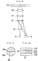
- Fig. 8 is a view showing a structure of a conventional optical pickup using a diffraction grating.
- light output from a semiconductor laser (laser diode) 34 is input to a first diffraction grating (referred to as a grating hereinafter) 35 and then separated to zero-order diffracted light (referred to as a main beam hereinafter) for reading an information signal and a pair of ⁇ 1-order diffracted light (referred to as a sub-beam hereinafter) for tracking which separates in a direction almost vertical to a paper surface.
- a semiconductor laser laser diode
- a second diffraction grating (referred to as a hologram hereinafter) 36, a collimator lens 37 and an objective lens 38 and then converge at a recording carrier (disc) 39. Then, the reflected light from the recording carrier 39 passes through the objective lens 38 and the collimator lens 37 and is then diffracted by the hologram 36 and its primary diffracted light is introduced to a photodetector 31.
- Figs. 9 and 10 are views showing a grating pattern of the hologram 36 viewed from the recording carrier 39 and a pattern at a light receiving part of the photodetector 31, respectively.
- the hologram 36 comprises two regions 36a and 36b and the receiving part of the receiving element 31 comprises five regions 31a to 31e.
- the main beam diffracted in the region 36a of the hologram converges on a line between the light receiving parts 31a and 31b and the main beam diffracted in the region 36b converges in the light receiving part 31c.
- two sub-beams converge in the light receiving parts 31d and 31e, respectively.
- received light is converted to a current signal corresponding to a light intensity by the photodetector 31.
- a current corresponding to each quantity of received light is generated from the light receiving parts 31a to 31e in the photodetector 31.
- the current is introduced into a current-voltage converting circuit positioned outside the optical pickup and converted to a voltage signal. Thereafter, a focus error signal (FES), a radial error signal (RES) and an information signal (RF) are generated by a signal operation circuit connected to the output of the current-voltage converting circuit.
- FES focus error signal
- RES radial error signal
- RF information signal
- the optical utilization factor of the above optical pickup is lower, while the above optical pickup is smaller and its weight is less as compared with an optical pickup using a beam splitter of a half mirror instead of a diffraction grating. More specifically, in a case where the half mirror is used, a quantity of light input to the photodetector becomes 25% when the light passes through the half mirror both ways. However, according to the pickup using the diffraction grating, a quantity of light is 14% at most when the light passes through the diffraction grating both ways. Thus, when the quantity of light becomes about half, an S/N ratio is deteriorated. The S/N ratio is likely to be deteriorated in the process of transmitting a signal from the photodetector 31 to the current-voltage converting circuit by a small current.
- the optical pickup using the holographic optical element whose signal level is about 1/2 can not be connected. Therefore, in a case where the optical pickup using the holographic optical element is used together with the signal processing circuit, an amplifying circuit for adjusting a gain has to be provided between the optical pickup and the signal processing circuit.
- JP-A-1-260637 discloses an optical pickup according to the preamble of claim 1.
- the object of the present invention is to provide an optical pickup using a holographic optical element in which an S/N ratio of an output signal from a photodetector can be improved.
- the present invention provides an optical pickup for an optical reproduction apparatus in which data recorded on a data carrier is read using an optical beam focused onto said carrier, the optical pickup comprising a photoelectric detecting means, a diffraction grating arranged for deflecting light reflected from the carrier toward the photoelectric detecting means, and circuitry coupled to the photoelectric detecting means for performing at least signal amplification, characterized in that said circuitry and said photoelectric detecting means are formed as an integrated circuit on the same semiconductor substrate.
- the S/N ratio is improved and, even if a diffraction grating whose light utilization factor is small is used, it is possible to obtain an output signal having a good S/N ratio.
- the overall structure except for a structure of a photodetector of an optical pickup in accordance with an embodiment of the present invention is the same as that shown in Fig. 8, so that its description is omitted.
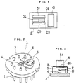
- Fig. 2 is a perspective view showing an inside structure of a laser unit in accordance with the embodiment of the present invention and Fig. 3 is a longitudinal sectional view showing the laser unit.
- a monitor photodiode 4 a laser diode 5 serving as a light source and a light receiving element 6 are arranged on a stem 3 having lead pins 2 for connection to the outside.
- a cap 9 having a cap glass 7 and a hologram glass 8 at the upper side so as to protect these elements is provided on the stem 3.
- the hologram glass 8 comprises a hologram pattern 8a and a grating pattern 8b.
- the photodetector 6 comprises five photodiodes D1, D2, D3, D4 and D5 and a signal processing circuit 10 which amplifies at least output signals from the photodiodes D1 to D5.
- Fig. 4 is a view showing a first structure of the signal processing circuit 10.
- a signal processing circuit 101 comprises transistors TR1, TR2, TR3, TR4 and TR5 which are provided corresponding to the photodiodes D1, D2, D3, D4 and D5, respectively. More specifically, a base of each of the transistors TR1 to TR5 is connected to an anode of each of the photodiodes D1 to D5 and each collector is connected to a cathode of each of the photodiodes D1 to D5 and to a power supply line 11 connected to an outside power supply. An emitter of each of the transistors TR1 to TR5 is connected to one of the pins 2 and becomes an output end of the photodetector 6.
- the signal processing circuit 101 is a current amplifying circuit which amplifies a current output corresponding to a quantity of light received by the photodiodes D1 to D5 and outputs the amplified current. Therefore, because the level of the output current of the photodetector 6 is larger than that of the conventional one, influence of disturbance is comparatively small and degradation of the S/N ratio is recuced.
- the level of the output current may be adjusted by adjusting the amplification degree of the transistors TR1 to TR5 in accordance with the input level of an I-V converting circuit of a later stage or the signal processing circuit.
- Fig. 5 is a view showing a second structure of the signal processing circuit 10.
- a signal processing circuit 102 is an I-V (current-voltage) converting circuit comprising operational amplifiers OP1, OP2, OP3, OP4 and OP5.
- An (-) input of each of the operational amplifiers OP1 to OP5 is connected to an anode of each of the photodiodes D1 to D5 and (+) input is connected to a ground GND.
- a current generated in each of the photodiodes D1 to D5 is converted to a voltage by each of the operational amplifiers OP1 to OP5 and then output.
- connection to the outside signal operating circuit can be easily implemented by setting the amplification degree of each of the operational amplifiers OP1 to OP5 in accordance with sensitivity of each of the photodiodes D1 to D5.
- Fig. 6 is a view showing a third structure of the signal processing circuit 10.
- a signal processing circuit 103 is an I-V converting and signal operation circuit comprising three operational amplifiers OP6, OP7 and OP8. More specifically, the operational amplifier OP6 performs operation in which the output current of the photodiode D1 is subtracted from the output current of the photodiode D5 to output the radial error signal RES.
- the operational amplifier OP7 performs addition by adding the output current of the photodiodes D2, D3 and 04 and then outputs the information signal RF.
- the operational amplifier OP8 performs subtraction by subtracting the output current of the photodiode D2 from the output current of the photodiode D3 and then outputs the focus error signal FES.
- the respective signals output from the signal processing circuit 103 are voltage signals. More specifically, in each of the operational amplifiers OP6, OP7 and OP8, current-voltage conversion, amplification and each operation are performed. Therefore, the output signal is not likely to be influenced by disturbance and deterioration of the S/N ratio is reduced.
- the signal is output in the form of the focus and radial error signals and the information signal, so that the outer circuit capable of being connected in this embodiment may be a common circuit which can process these signals. Thus, for example, it is not necessary to consider a difference of operation process of generation of the focus error signal when the outer circuit is determined.
- Fig. 7 is a view showing a fourth structure of the signal processing circuit 10.
- a signal processing circuit 104 comprises five operational amplifiers OP11 to OP15, resistors R1 to R3 and capacitors C1 to C3.
- the operational amplifier OP11 converts the output current of the photodiodes 02, 03 and D4 to a voltage and also adds and outputs them.
- the capacitors C1 to C3 are for DC cutting.
- the operational amplifiers OP12 to OP15 operate as I-V converting circuits. More specifically, they amplify the current signals output from the photodiodes D1, 02, D3 and D5 and also convert them to a voltage and then output them.
- the output signal of the photodiode D4 is not output alone. More specifically, the signal processing circuit 104 outputs the information signal RF (V RF ), so that the radial and focus error signals necessary for servo control can be operated by the output signals of the photodiodes D1, 02, D3 and D5.
- V RF information signal
- the photodetector in the above embodiments of the present invention is manufactured by forming the photodiode and the signal processing circuit on the same semiconductor substrate.
- the manufacturing process well-known technique of manufacturing an integrated circuit is used.
Landscapes
- Physics & Mathematics (AREA)
- Optics & Photonics (AREA)
- Optical Head (AREA)
- Photometry And Measurement Of Optical Pulse Characteristics (AREA)
Description
- The present invention relates to an optical pickup used in an apparatus for recording and reproducing an optical memory such as a compact disc player or a video disc player and, more particularly, to an optical pickup using a holographic optical element in an optical system in order to reduce size and weight.
- Fig. 8 is a view showing a structure of a conventional optical pickup using a diffraction grating. In Fig. 8, light output from a semiconductor laser (laser diode) 34 is input to a first diffraction grating (referred to as a grating hereinafter) 35 and then separated to zero-order diffracted light (referred to as a main beam hereinafter) for reading an information signal and a pair of ±1-order diffracted light (referred to as a sub-beam hereinafter) for tracking which separates in a direction almost vertical to a paper surface. These three beams pass through a second diffraction grating (referred to as a hologram hereinafter) 36, a
collimator lens 37 and anobjective lens 38 and then converge at a recording carrier (disc) 39. Then, the reflected light from therecording carrier 39 passes through theobjective lens 38 and thecollimator lens 37 and is then diffracted by thehologram 36 and its primary diffracted light is introduced to aphotodetector 31. - Figs. 9 and 10 are views showing a grating pattern of the
hologram 36 viewed from therecording carrier 39 and a pattern at a light receiving part of thephotodetector 31, respectively. Thehologram 36 comprises tworegions 36a and 36b and the receiving part of the receivingelement 31 comprises fiveregions 31a to 31e. The main beam diffracted in the region 36a of the hologram converges on a line between the light receivingparts region 36b converges in thelight receiving part 31c. Then, two sub-beams converge in thelight receiving parts photodetector 31. - A current corresponding to each quantity of received light is generated from the
light receiving parts 31a to 31e in thephotodetector 31. The current is introduced into a current-voltage converting circuit positioned outside the optical pickup and converted to a voltage signal. Thereafter, a focus error signal (FES), a radial error signal (RES) and an information signal (RF) are generated by a signal operation circuit connected to the output of the current-voltage converting circuit. At this time, when signals output from thelight receiving part - A structure of such an optical pickup using a holographic optical element is disclosed in Japanese Laid-Open Patent Publication No. 151022/1989.
- However, the optical utilization factor of the above optical pickup is lower, while the above optical pickup is smaller and its weight is less as compared with an optical pickup using a beam splitter of a half mirror instead of a diffraction grating. More specifically, in a case where the half mirror is used, a quantity of light input to the photodetector becomes 25% when the light passes through the half mirror both ways. However, according to the pickup using the diffraction grating, a quantity of light is 14% at most when the light passes through the diffraction grating both ways. Thus, when the quantity of light becomes about half, an S/N ratio is deteriorated. The S/N ratio is likely to be deteriorated in the process of transmitting a signal from the
photodetector 31 to the current-voltage converting circuit by a small current. - In addition, in a case where the signal processing circuit used together with the optical pickup is integrated corresponding to a signal level of the half mirror type optical pickup, the optical pickup using the holographic optical element whose signal level is about 1/2 can not be connected. Therefore, in a case where the optical pickup using the holographic optical element is used together with the signal processing circuit, an amplifying circuit for adjusting a gain has to be provided between the optical pickup and the signal processing circuit.
- JP-A-1-260637 discloses an optical pickup according to the preamble of
claim 1. - The object of the present invention is to provide an optical pickup using a holographic optical element in which an S/N ratio of an output signal from a photodetector can be improved.
- The present invention provides an optical pickup for an optical reproduction apparatus in which data recorded on a data carrier is read using an optical beam focused onto said carrier, the optical pickup comprising a photoelectric detecting means, a diffraction grating arranged for deflecting light reflected from the carrier toward the photoelectric detecting means, and circuitry coupled to the photoelectric detecting means for performing at least signal amplification, characterized in that said circuitry and said photoelectric detecting means are formed as an integrated circuit on the same semiconductor substrate.
- According to the present invention, the S/N ratio is improved and, even if a diffraction grating whose light utilization factor is small is used, it is possible to obtain an output signal having a good S/N ratio.
- Several embodiments of the invention will now be described by way of example and with reference to the accompanying drawings, in which:
- Fig. 1 is a plan view showing a structure of a photodetector of an embodiment of the present invention;
- Figs. 2 and 3 are a perspective view and partially omitted longitudinal sectional view, respectively, each showing a structure of a laser unit of the embodiment of the present invention;
- Fig. 4 is a circuit diagram showing a structure of a signal processing circuit in accordance with a first embodiment of the present invention;
- Fig. 5 is a circuit diagram showing a structure of a signal processing circuit in accordance with a second embodiment of the present invention;
- Fig. 6 is a circuit diagram showing a structure of a signal processing circuit in accordance with a third embodiment of the present invention;
- Fig. 7 is a circuit diagram showing a structure of a signal processing circuit in accordance with a fourth embodiment of the present invention;
- Fig. 8 is a schematic view showing a whole structure of an optical pickup;
- Fig. 9 is a plan view showing a grating pattern of a hologram of the optical pickup; and
- Fig. 10 is a plan view showing a pattern at a light receiving part of a conventional photodetector.
- The overall structure except for a structure of a photodetector of an optical pickup in accordance with an embodiment of the present invention is the same as that shown in Fig. 8, so that its description is omitted.
- Fig. 2 is a perspective view showing an inside structure of a laser unit in accordance with the embodiment of the present invention and Fig. 3 is a longitudinal sectional view showing the laser unit.
- In the
laser unit 1, amonitor photodiode 4, alaser diode 5 serving as a light source and a light receivingelement 6 are arranged on astem 3 havinglead pins 2 for connection to the outside. In addition, acap 9 having acap glass 7 and ahologram glass 8 at the upper side so as to protect these elements is provided on thestem 3. Thehologram glass 8 comprises ahologram pattern 8a and agrating pattern 8b. - As shown in Fig. 1, the
photodetector 6 comprises five photodiodes D1, D2, D3, D4 and D5 and asignal processing circuit 10 which amplifies at least output signals from the photodiodes D1 to D5. - Fig. 4 is a view showing a first structure of the
signal processing circuit 10. In Fig. 4, asignal processing circuit 101 comprises transistors TR1, TR2, TR3, TR4 and TR5 which are provided corresponding to the photodiodes D1, D2, D3, D4 and D5, respectively. More specifically, a base of each of the transistors TR1 to TR5 is connected to an anode of each of the photodiodes D1 to D5 and each collector is connected to a cathode of each of the photodiodes D1 to D5 and to apower supply line 11 connected to an outside power supply. An emitter of each of the transistors TR1 to TR5 is connected to one of thepins 2 and becomes an output end of thephotodetector 6. - The
signal processing circuit 101 is a current amplifying circuit which amplifies a current output corresponding to a quantity of light received by the photodiodes D1 to D5 and outputs the amplified current. Therefore, because the level of the output current of thephotodetector 6 is larger than that of the conventional one, influence of disturbance is comparatively small and degradation of the S/N ratio is recuced. The level of the output current may be adjusted by adjusting the amplification degree of the transistors TR1 to TR5 in accordance with the input level of an I-V converting circuit of a later stage or the signal processing circuit. - Fig. 5 is a view showing a second structure of the
signal processing circuit 10. In Fig. 5, asignal processing circuit 102 is an I-V (current-voltage) converting circuit comprising operational amplifiers OP1, OP2, OP3, OP4 and OP5. An (-) input of each of the operational amplifiers OP1 to OP5 is connected to an anode of each of the photodiodes D1 to D5 and (+) input is connected to a ground GND. - A current generated in each of the photodiodes D1 to D5 is converted to a voltage by each of the operational amplifiers OP1 to OP5 and then output. In this case, connection to the outside signal operating circuit can be easily implemented by setting the amplification degree of each of the operational amplifiers OP1 to OP5 in accordance with sensitivity of each of the photodiodes D1 to D5.
- Fig. 6 is a view showing a third structure of the
signal processing circuit 10. In Fig. 6, asignal processing circuit 103 is an I-V converting and signal operation circuit comprising three operational amplifiers OP6, OP7 and OP8. More specifically, the operational amplifier OP6 performs operation in which the output current of the photodiode D1 is subtracted from the output current of the photodiode D5 to output the radial error signal RES. The operational amplifier OP7 performs addition by adding the output current of the photodiodes D2, D3 and 04 and then outputs the information signal RF. In additian, the operational amplifier OP8 performs subtraction by subtracting the output current of the photodiode D2 from the output current of the photodiode D3 and then outputs the focus error signal FES. - In this third structure, the respective signals output from the
signal processing circuit 103 are voltage signals. More specifically, in each of the operational amplifiers OP6, OP7 and OP8, current-voltage conversion, amplification and each operation are performed. Therefore, the output signal is not likely to be influenced by disturbance and deterioration of the S/N ratio is reduced. In addition, the signal is output in the form of the focus and radial error signals and the information signal, so that the outer circuit capable of being connected in this embodiment may be a common circuit which can process these signals. Thus, for example, it is not necessary to consider a difference of operation process of generation of the focus error signal when the outer circuit is determined. - Fig. 7 is a view showing a fourth structure of the
signal processing circuit 10. - In Fig. 7, a
signal processing circuit 104 comprises five operational amplifiers OP11 to OP15, resistors R1 to R3 and capacitors C1 to C3. The operational amplifier OP11 converts the output current of the photodiodes 02, 03 and D4 to a voltage and also adds and outputs them. The capacitors C1 to C3 are for DC cutting. The operational amplifiers OP12 to OP15 operate as I-V converting circuits. More specifically, they amplify the current signals output from the photodiodes D1, 02, D3 and D5 and also convert them to a voltage and then output them. - In the fourth structure, the output signal of the photodiode D4 is not output alone. More specifically, the
signal processing circuit 104 outputs the information signal RF (VRF), so that the radial and focus error signals necessary for servo control can be operated by the output signals of the photodiodes D1, 02, D3 and D5. Thus, in this structure, various signal operating circuits can be connected. - In addition, the photodetector in the above embodiments of the present invention is manufactured by forming the photodiode and the signal processing circuit on the same semiconductor substrate. In the manufacturing process, well-known technique of manufacturing an integrated circuit is used.
- While only certain presently preferred embodiments have been described in detail, as will be apparent to those skilled in the art, certain changes and modifications can be made without departing from the scope of the invention as defined by the following claims.
Claims (5)
- An optical pickup for an optical reproduction apparatus in which data recorded on a data carrier is read using an optical beam focused onto said carrier, the optical pickup comprising a photoelectric detecting means (D1-D5), a diffraction grating (8a) arranged for deflecting light reflected from the carrier toward the photoelectric detecting means, and circuitry (10:101;102; 103;104) coupled to the photoelectric detecting means for performing at least signal amplification, characterized in that said circuitry (10) and said photoelectric detecting means (D1-D5) are formed as an integrated circuit on the same semiconductor substrate (6).
- An optical pickup according to claim 1, further comprising a base plate (3) on which said semiconductor substrate (6) is mounted, and electrical connection elements (2) supported by said base plate and connected to said circuitry, for coupling amplified signals derived from the photoelectric detecting means to external circuitry.
- An optical pickup according to claim 1 or claim 2, wherein said circuitry (10:103;104) performs signal processing to generate servo control signals (RES,FES).
- An optical pickup according to any of claims 1 to 3, wherein said circuitry (10:102;103;104) performs current-to-voltage conversion.
- An optical pickup according to any of claims 1 to 4, wherein said photoelectric detecting means comprises a plurality of photodiodes (D1-D5).
Applications Claiming Priority (2)
| Application Number | Priority Date | Filing Date | Title |
|---|---|---|---|
| JP262100/90 | 1990-09-27 | ||
| JP2262100A JPH04137232A (en) | 1990-09-27 | 1990-09-27 | Optical pickup device |
Publications (3)
| Publication Number | Publication Date |
|---|---|
| EP0478222A2 EP0478222A2 (en) | 1992-04-01 |
| EP0478222A3 EP0478222A3 (en) | 1992-12-16 |
| EP0478222B1 true EP0478222B1 (en) | 1997-06-11 |
Family
ID=17371038
Family Applications (1)
| Application Number | Title | Priority Date | Filing Date |
|---|---|---|---|
| EP91308539A Expired - Lifetime EP0478222B1 (en) | 1990-09-27 | 1991-09-19 | Optical pickup using a holographic optical element |
Country Status (4)
| Country | Link |
|---|---|
| US (1) | US5272329A (en) |
| EP (1) | EP0478222B1 (en) |
| JP (1) | JPH04137232A (en) |
| DE (1) | DE69126496T2 (en) |
Families Citing this family (7)
| Publication number | Priority date | Publication date | Assignee | Title |
|---|---|---|---|---|
| EP0598592B1 (en) * | 1992-11-17 | 1999-09-01 | Seiko Epson Corporation | Optical head |
| JPH07176095A (en) * | 1993-06-25 | 1995-07-14 | Nec Corp | Magneto-optical head device |
| DE69621678T2 (en) * | 1995-03-14 | 2002-11-28 | Kabushiki Kaisha Toshiba, Kawasaki | light detector |
| JPH10172173A (en) * | 1996-12-06 | 1998-06-26 | Samsung Electron Co Ltd | Optical pickup device |
| JPH11213441A (en) * | 1998-01-23 | 1999-08-06 | Rohm Co Ltd | Optical pickup and its adjusting method |
| KR20060093115A (en) * | 2003-10-21 | 2006-08-23 | 코닌클리케 필립스 일렉트로닉스 엔.브이. | Optical disc drive |
| DE102004035494A1 (en) * | 2004-07-22 | 2006-02-09 | Giesecke & Devrient Gmbh | Device and method for checking value documents |
Citations (3)
| Publication number | Priority date | Publication date | Assignee | Title |
|---|---|---|---|---|
| JPH01260637A (en) * | 1988-04-12 | 1989-10-17 | Sharp Corp | Tracking error detecting device for optical pickup |
| JPH0224841A (en) * | 1988-07-14 | 1990-01-26 | Toshiba Corp | Optical information processor |
| EP0400754A1 (en) * | 1989-06-02 | 1990-12-05 | Koninklijke Philips Electronics N.V. | Photosensitive semiconductor device |
Family Cites Families (15)
| Publication number | Priority date | Publication date | Assignee | Title |
|---|---|---|---|---|
| US4125860A (en) * | 1975-06-16 | 1978-11-14 | Nippon Telegraph And Telephone Public Corporation | Reproducer for an eraseable videodisc |
| EP0099651A3 (en) * | 1981-07-23 | 1984-03-21 | Comtech Research Unit Limited | Optical data storage |
| JPH0246923B2 (en) * | 1984-10-13 | 1990-10-17 | Sumitomo Beekuraito Kk | HIKARIFUAIBAAKONEKUTAA |
| US4885732A (en) * | 1986-09-02 | 1989-12-05 | Fuji Photo Film Co., Ltd. | Optical pickup apparatus for detecting and correcting focusing and tracking errors in detected recorded signals |
| JPH0675307B2 (en) * | 1987-01-30 | 1994-09-21 | 富士写真フイルム株式会社 | Pickup for magneto-optical recording medium |
| EP0288033B1 (en) * | 1987-04-20 | 1993-04-07 | Fuji Photo Film Co., Ltd. | Pickup apparatus for magneto-optical recording medium |
| NL8702245A (en) * | 1987-09-21 | 1989-04-17 | Philips Nv | DEVICE FOR SCANNING A RADIATION-REFLECTING INFORMATION SHEET WITH OPTICAL RADIATION. |
| EP0311340B1 (en) * | 1987-10-05 | 1993-08-04 | Matsushita Electric Industrial Co., Ltd. | Optical pickup head |
| JPH01151022A (en) * | 1987-12-09 | 1989-06-13 | Sharp Corp | Optical pick-up device |
| JPH01303639A (en) * | 1988-05-31 | 1989-12-07 | Nec Home Electron Ltd | Hologram optical head |
| JPH01313987A (en) * | 1988-06-14 | 1989-12-19 | Sharp Corp | Integration type laser unit |
| JPH0266727A (en) * | 1988-08-31 | 1990-03-06 | Toshiba Corp | Electronic equipment |
| US5049732A (en) * | 1988-10-21 | 1991-09-17 | Sharp Kabushiki Kaisha | Optical pickup device with diffraction device |
| NL8802988A (en) * | 1988-12-05 | 1990-07-02 | Philips Nv | DEVICE FOR SCANNING AN INFORMATION SHEET WITH OPTICAL RADIATION. |
| JPH06103543B2 (en) * | 1988-12-31 | 1994-12-14 | 三星電子株式会社 | Laser pickup |
-
1990
- 1990-09-27 JP JP2262100A patent/JPH04137232A/en active Pending
-
1991
- 1991-09-19 EP EP91308539A patent/EP0478222B1/en not_active Expired - Lifetime
- 1991-09-19 US US07/762,420 patent/US5272329A/en not_active Expired - Lifetime
- 1991-09-19 DE DE69126496T patent/DE69126496T2/en not_active Expired - Fee Related
Patent Citations (3)
| Publication number | Priority date | Publication date | Assignee | Title |
|---|---|---|---|---|
| JPH01260637A (en) * | 1988-04-12 | 1989-10-17 | Sharp Corp | Tracking error detecting device for optical pickup |
| JPH0224841A (en) * | 1988-07-14 | 1990-01-26 | Toshiba Corp | Optical information processor |
| EP0400754A1 (en) * | 1989-06-02 | 1990-12-05 | Koninklijke Philips Electronics N.V. | Photosensitive semiconductor device |
Also Published As
| Publication number | Publication date |
|---|---|
| DE69126496T2 (en) | 1998-01-08 |
| DE69126496D1 (en) | 1997-07-17 |
| JPH04137232A (en) | 1992-05-12 |
| US5272329A (en) | 1993-12-21 |
| EP0478222A3 (en) | 1992-12-16 |
| EP0478222A2 (en) | 1992-04-01 |
Similar Documents
| Publication | Publication Date | Title |
|---|---|---|
| US6731585B2 (en) | Optical pick-up head with semiconductor laser | |
| EP0565052A1 (en) | Optical pick-up head apparatus wherein holographic optical element and photodetector are formed on semiconductor substrate | |
| US20080205820A1 (en) | Dynamically configurable multiple wavelength photodetector array for optical storage applications | |
| US5272329A (en) | Optical pickup device using a holographic optical element and an amplifier | |
| WO1996024131A1 (en) | Optical signal detection circuit | |
| JP2009252330A (en) | Optical signal detecting circuit and information reproducing device using same | |
| US6212150B1 (en) | Optical pickup apparatus and optical recording medium drive employing the same including a first photo receiving element for detecting the state of light beam and a second photo receiving element for reproducing information | |
| KR100933291B1 (en) | Photodetectors for the Use of Two-Wave Laser Diodes | |
| JP4902337B2 (en) | Optical pickup and optical information reproducing apparatus | |
| US20060261243A1 (en) | Optical reproducing apparatus capable of using laser diode of two wavelengths | |
| US5253240A (en) | Tracking error detecting system for removing an offset in an optical disk player | |
| KR100198052B1 (en) | Tilt error control device | |
| JPH01112534A (en) | Optical pickup device | |
| JPH06303061A (en) | Adjustment device for electronic device | |
| US5537386A (en) | Tracking and focusing servo driven by comparison of direct current signals rectified from detectors | |
| JP3090086B2 (en) | Photodetector with built-in circuit | |
| JPH02289929A (en) | Semiconductor integrated circuit | |
| JP4378704B2 (en) | Optical pickup | |
| JP4425485B2 (en) | Optical pickup head and information recording / reproducing apparatus | |
| JP2006209874A (en) | Photodetection device, optical pickup and optical disk device | |
| US20070035801A1 (en) | Light receiving element circuit and optical disk device | |
| KR20060064331A (en) | PDC circuit capable of mode switching | |
| JPH09115168A (en) | Light emitting / receiving element | |
| JPS6111942A (en) | Recording information detecting device | |
| JP2007519127A (en) | Optical disk drive |
Legal Events
| Date | Code | Title | Description |
|---|---|---|---|
| PUAI | Public reference made under article 153(3) epc to a published international application that has entered the european phase |
Free format text: ORIGINAL CODE: 0009012 |
|
| AK | Designated contracting states |
Kind code of ref document: A2 Designated state(s): DE FR GB NL |
|
| PUAL | Search report despatched |
Free format text: ORIGINAL CODE: 0009013 |
|
| AK | Designated contracting states |
Kind code of ref document: A3 Designated state(s): DE FR GB NL |
|
| 17P | Request for examination filed |
Effective date: 19930209 |
|
| 17Q | First examination report despatched |
Effective date: 19941212 |
|
| GRAG | Despatch of communication of intention to grant |
Free format text: ORIGINAL CODE: EPIDOS AGRA |
|
| GRAH | Despatch of communication of intention to grant a patent |
Free format text: ORIGINAL CODE: EPIDOS IGRA |
|
| GRAH | Despatch of communication of intention to grant a patent |
Free format text: ORIGINAL CODE: EPIDOS IGRA |
|
| GRAA | (expected) grant |
Free format text: ORIGINAL CODE: 0009210 |
|
| AK | Designated contracting states |
Kind code of ref document: B1 Designated state(s): DE FR GB NL |
|
| REF | Corresponds to: |
Ref document number: 69126496 Country of ref document: DE Date of ref document: 19970717 |
|
| ET | Fr: translation filed | ||
| PLBE | No opposition filed within time limit |
Free format text: ORIGINAL CODE: 0009261 |
|
| STAA | Information on the status of an ep patent application or granted ep patent |
Free format text: STATUS: NO OPPOSITION FILED WITHIN TIME LIMIT |
|
| 26N | No opposition filed | ||
| REG | Reference to a national code |
Ref country code: GB Ref legal event code: IF02 |
|
| PGFP | Annual fee paid to national office [announced via postgrant information from national office to epo] |
Ref country code: FR Payment date: 20080915 Year of fee payment: 18 Ref country code: NL Payment date: 20080915 Year of fee payment: 18 |
|
| PGFP | Annual fee paid to national office [announced via postgrant information from national office to epo] |
Ref country code: GB Payment date: 20080924 Year of fee payment: 18 |
|
| PGFP | Annual fee paid to national office [announced via postgrant information from national office to epo] |
Ref country code: DE Payment date: 20081002 Year of fee payment: 18 |
|
| REG | Reference to a national code |
Ref country code: NL Ref legal event code: V1 Effective date: 20100401 |
|
| GBPC | Gb: european patent ceased through non-payment of renewal fee |
Effective date: 20090919 |
|
| REG | Reference to a national code |
Ref country code: FR Ref legal event code: ST Effective date: 20100531 |
|
| PG25 | Lapsed in a contracting state [announced via postgrant information from national office to epo] |
Ref country code: NL Free format text: LAPSE BECAUSE OF NON-PAYMENT OF DUE FEES Effective date: 20100401 Ref country code: DE Free format text: LAPSE BECAUSE OF NON-PAYMENT OF DUE FEES Effective date: 20100401 Ref country code: FR Free format text: LAPSE BECAUSE OF NON-PAYMENT OF DUE FEES Effective date: 20090930 |
|
| PG25 | Lapsed in a contracting state [announced via postgrant information from national office to epo] |
Ref country code: GB Free format text: LAPSE BECAUSE OF NON-PAYMENT OF DUE FEES Effective date: 20090919 |