EP0478174A2 - Silicon dioxide deposition method and apparatus - Google Patents
Silicon dioxide deposition method and apparatus Download PDFInfo
- Publication number
- EP0478174A2 EP0478174A2 EP91308268A EP91308268A EP0478174A2 EP 0478174 A2 EP0478174 A2 EP 0478174A2 EP 91308268 A EP91308268 A EP 91308268A EP 91308268 A EP91308268 A EP 91308268A EP 0478174 A2 EP0478174 A2 EP 0478174A2
- Authority
- EP
- European Patent Office
- Prior art keywords
- silicon dioxide
- layer
- substrate
- magnetic field
- further characterized
- Prior art date
- Legal status (The legal status is an assumption and is not a legal conclusion. Google has not performed a legal analysis and makes no representation as to the accuracy of the status listed.)
- Granted
Links
- VYPSYNLAJGMNEJ-UHFFFAOYSA-N Silicium dioxide Chemical compound O=[Si]=O VYPSYNLAJGMNEJ-UHFFFAOYSA-N 0.000 title claims abstract description 140
- 235000012239 silicon dioxide Nutrition 0.000 title claims abstract description 71
- 239000000377 silicon dioxide Substances 0.000 title claims abstract description 69
- 238000000151 deposition Methods 0.000 title claims abstract description 55
- 230000008021 deposition Effects 0.000 claims abstract description 41
- 239000000758 substrate Substances 0.000 claims abstract description 20
- 238000000034 method Methods 0.000 claims description 23
- 238000004544 sputter deposition Methods 0.000 claims description 20
- 230000015572 biosynthetic process Effects 0.000 claims description 13
- 239000007789 gas Substances 0.000 claims description 13
- MWUXSHHQAYIFBG-UHFFFAOYSA-N Nitric oxide Chemical compound O=[N] MWUXSHHQAYIFBG-UHFFFAOYSA-N 0.000 claims description 9
- XUIMIQQOPSSXEZ-UHFFFAOYSA-N Silicon Chemical compound [Si] XUIMIQQOPSSXEZ-UHFFFAOYSA-N 0.000 claims description 9
- 229910052710 silicon Inorganic materials 0.000 claims description 9
- 239000010703 silicon Substances 0.000 claims description 9
- BOTDANWDWHJENH-UHFFFAOYSA-N Tetraethyl orthosilicate Chemical compound CCO[Si](OCC)(OCC)OCC BOTDANWDWHJENH-UHFFFAOYSA-N 0.000 claims description 8
- QVGXLLKOCUKJST-UHFFFAOYSA-N atomic oxygen Chemical compound [O] QVGXLLKOCUKJST-UHFFFAOYSA-N 0.000 claims description 7
- 239000001301 oxygen Substances 0.000 claims description 7
- 229910052760 oxygen Inorganic materials 0.000 claims description 7
- BLRPTPMANUNPDV-UHFFFAOYSA-N Silane Chemical compound [SiH4] BLRPTPMANUNPDV-UHFFFAOYSA-N 0.000 claims description 5
- 229910000077 silane Inorganic materials 0.000 claims description 4
- MYMOFIZGZYHOMD-UHFFFAOYSA-N Dioxygen Chemical compound O=O MYMOFIZGZYHOMD-UHFFFAOYSA-N 0.000 claims description 2
- 239000011261 inert gas Substances 0.000 claims 4
- 239000004020 conductor Substances 0.000 abstract description 37
- 238000000623 plasma-assisted chemical vapour deposition Methods 0.000 abstract description 8
- 229910052751 metal Inorganic materials 0.000 abstract description 4
- 239000002184 metal Substances 0.000 abstract description 4
- 235000012431 wafers Nutrition 0.000 description 28
- 238000005516 engineering process Methods 0.000 description 5
- 230000001965 increasing effect Effects 0.000 description 5
- 238000004519 manufacturing process Methods 0.000 description 5
- 239000000463 material Substances 0.000 description 5
- XKRFYHLGVUSROY-UHFFFAOYSA-N Argon Chemical compound [Ar] XKRFYHLGVUSROY-UHFFFAOYSA-N 0.000 description 4
- 230000003749 cleanliness Effects 0.000 description 4
- 150000002500 ions Chemical class 0.000 description 4
- 239000004065 semiconductor Substances 0.000 description 4
- 238000013459 approach Methods 0.000 description 3
- 238000009413 insulation Methods 0.000 description 3
- 239000007788 liquid Substances 0.000 description 3
- 239000000203 mixture Substances 0.000 description 3
- 238000000926 separation method Methods 0.000 description 3
- 238000000992 sputter etching Methods 0.000 description 3
- 238000012546 transfer Methods 0.000 description 3
- GQPLMRYTRLFLPF-UHFFFAOYSA-N Nitrous Oxide Chemical compound [O-][N+]#N GQPLMRYTRLFLPF-UHFFFAOYSA-N 0.000 description 2
- 229910052786 argon Inorganic materials 0.000 description 2
- 230000008901 benefit Effects 0.000 description 2
- 238000005229 chemical vapour deposition Methods 0.000 description 2
- 230000008018 melting Effects 0.000 description 2
- 238000002844 melting Methods 0.000 description 2
- 238000012986 modification Methods 0.000 description 2
- 230000004048 modification Effects 0.000 description 2
- 239000010453 quartz Substances 0.000 description 2
- LIVNPJMFVYWSIS-UHFFFAOYSA-N silicon monoxide Chemical compound [Si-]#[O+] LIVNPJMFVYWSIS-UHFFFAOYSA-N 0.000 description 2
- OKTJSMMVPCPJKN-UHFFFAOYSA-N Carbon Chemical group [C] OKTJSMMVPCPJKN-UHFFFAOYSA-N 0.000 description 1
- 230000002411 adverse Effects 0.000 description 1
- XKRFYHLGVUSROY-AHCXROLUSA-N argon-36 Chemical compound [36Ar] XKRFYHLGVUSROY-AHCXROLUSA-N 0.000 description 1
- 230000005540 biological transmission Effects 0.000 description 1
- 230000005587 bubbling Effects 0.000 description 1
- 239000011248 coating agent Substances 0.000 description 1
- 238000000576 coating method Methods 0.000 description 1
- 229910052681 coesite Inorganic materials 0.000 description 1
- 229910052906 cristobalite Inorganic materials 0.000 description 1
- 238000012864 cross contamination Methods 0.000 description 1
- 238000013461 design Methods 0.000 description 1
- 229910001882 dioxygen Inorganic materials 0.000 description 1
- 238000009826 distribution Methods 0.000 description 1
- 230000000694 effects Effects 0.000 description 1
- 230000002708 enhancing effect Effects 0.000 description 1
- 238000005530 etching Methods 0.000 description 1
- 238000002474 experimental method Methods 0.000 description 1
- 238000000227 grinding Methods 0.000 description 1
- 239000001307 helium Substances 0.000 description 1
- 229910052734 helium Inorganic materials 0.000 description 1
- SWQJXJOGLNCZEY-UHFFFAOYSA-N helium atom Chemical compound [He] SWQJXJOGLNCZEY-UHFFFAOYSA-N 0.000 description 1
- TWNQGVIAIRXVLR-UHFFFAOYSA-N oxo(oxoalumanyloxy)alumane Chemical compound O=[Al]O[Al]=O TWNQGVIAIRXVLR-UHFFFAOYSA-N 0.000 description 1
- 238000003825 pressing Methods 0.000 description 1
- 238000012545 processing Methods 0.000 description 1
- 229910052682 stishovite Inorganic materials 0.000 description 1
- 229910052905 tridymite Inorganic materials 0.000 description 1
- 239000011800 void material Substances 0.000 description 1
Images


Classifications
-
- H—ELECTRICITY
- H01—ELECTRIC ELEMENTS
- H01L—SEMICONDUCTOR DEVICES NOT COVERED BY CLASS H10
- H01L21/00—Processes or apparatus adapted for the manufacture or treatment of semiconductor or solid state devices or of parts thereof
- H01L21/02—Manufacture or treatment of semiconductor devices or of parts thereof
- H01L21/02104—Forming layers
- H01L21/02107—Forming insulating materials on a substrate
- H01L21/02109—Forming insulating materials on a substrate characterised by the type of layer, e.g. type of material, porous/non-porous, pre-cursors, mixtures or laminates
- H01L21/02112—Forming insulating materials on a substrate characterised by the type of layer, e.g. type of material, porous/non-porous, pre-cursors, mixtures or laminates characterised by the material of the layer
- H01L21/02123—Forming insulating materials on a substrate characterised by the type of layer, e.g. type of material, porous/non-porous, pre-cursors, mixtures or laminates characterised by the material of the layer the material containing silicon
- H01L21/02164—Forming insulating materials on a substrate characterised by the type of layer, e.g. type of material, porous/non-porous, pre-cursors, mixtures or laminates characterised by the material of the layer the material containing silicon the material being a silicon oxide, e.g. SiO2
-
- C—CHEMISTRY; METALLURGY
- C23—COATING METALLIC MATERIAL; COATING MATERIAL WITH METALLIC MATERIAL; CHEMICAL SURFACE TREATMENT; DIFFUSION TREATMENT OF METALLIC MATERIAL; COATING BY VACUUM EVAPORATION, BY SPUTTERING, BY ION IMPLANTATION OR BY CHEMICAL VAPOUR DEPOSITION, IN GENERAL; INHIBITING CORROSION OF METALLIC MATERIAL OR INCRUSTATION IN GENERAL
- C23C—COATING METALLIC MATERIAL; COATING MATERIAL WITH METALLIC MATERIAL; SURFACE TREATMENT OF METALLIC MATERIAL BY DIFFUSION INTO THE SURFACE, BY CHEMICAL CONVERSION OR SUBSTITUTION; COATING BY VACUUM EVAPORATION, BY SPUTTERING, BY ION IMPLANTATION OR BY CHEMICAL VAPOUR DEPOSITION, IN GENERAL
- C23C16/00—Chemical coating by decomposition of gaseous compounds, without leaving reaction products of surface material in the coating, i.e. chemical vapour deposition [CVD] processes
- C23C16/02—Pretreatment of the material to be coated
- C23C16/0272—Deposition of sub-layers, e.g. to promote the adhesion of the main coating
-
- C—CHEMISTRY; METALLURGY
- C23—COATING METALLIC MATERIAL; COATING MATERIAL WITH METALLIC MATERIAL; CHEMICAL SURFACE TREATMENT; DIFFUSION TREATMENT OF METALLIC MATERIAL; COATING BY VACUUM EVAPORATION, BY SPUTTERING, BY ION IMPLANTATION OR BY CHEMICAL VAPOUR DEPOSITION, IN GENERAL; INHIBITING CORROSION OF METALLIC MATERIAL OR INCRUSTATION IN GENERAL
- C23C—COATING METALLIC MATERIAL; COATING MATERIAL WITH METALLIC MATERIAL; SURFACE TREATMENT OF METALLIC MATERIAL BY DIFFUSION INTO THE SURFACE, BY CHEMICAL CONVERSION OR SUBSTITUTION; COATING BY VACUUM EVAPORATION, BY SPUTTERING, BY ION IMPLANTATION OR BY CHEMICAL VAPOUR DEPOSITION, IN GENERAL
- C23C16/00—Chemical coating by decomposition of gaseous compounds, without leaving reaction products of surface material in the coating, i.e. chemical vapour deposition [CVD] processes
- C23C16/22—Chemical coating by decomposition of gaseous compounds, without leaving reaction products of surface material in the coating, i.e. chemical vapour deposition [CVD] processes characterised by the deposition of inorganic material, other than metallic material
- C23C16/30—Deposition of compounds, mixtures or solid solutions, e.g. borides, carbides, nitrides
- C23C16/40—Oxides
- C23C16/401—Oxides containing silicon
- C23C16/402—Silicon dioxide
-
- C—CHEMISTRY; METALLURGY
- C23—COATING METALLIC MATERIAL; COATING MATERIAL WITH METALLIC MATERIAL; CHEMICAL SURFACE TREATMENT; DIFFUSION TREATMENT OF METALLIC MATERIAL; COATING BY VACUUM EVAPORATION, BY SPUTTERING, BY ION IMPLANTATION OR BY CHEMICAL VAPOUR DEPOSITION, IN GENERAL; INHIBITING CORROSION OF METALLIC MATERIAL OR INCRUSTATION IN GENERAL
- C23C—COATING METALLIC MATERIAL; COATING MATERIAL WITH METALLIC MATERIAL; SURFACE TREATMENT OF METALLIC MATERIAL BY DIFFUSION INTO THE SURFACE, BY CHEMICAL CONVERSION OR SUBSTITUTION; COATING BY VACUUM EVAPORATION, BY SPUTTERING, BY ION IMPLANTATION OR BY CHEMICAL VAPOUR DEPOSITION, IN GENERAL
- C23C16/00—Chemical coating by decomposition of gaseous compounds, without leaving reaction products of surface material in the coating, i.e. chemical vapour deposition [CVD] processes
- C23C16/44—Chemical coating by decomposition of gaseous compounds, without leaving reaction products of surface material in the coating, i.e. chemical vapour deposition [CVD] processes characterised by the method of coating
- C23C16/50—Chemical coating by decomposition of gaseous compounds, without leaving reaction products of surface material in the coating, i.e. chemical vapour deposition [CVD] processes characterised by the method of coating using electric discharges
- C23C16/505—Chemical coating by decomposition of gaseous compounds, without leaving reaction products of surface material in the coating, i.e. chemical vapour deposition [CVD] processes characterised by the method of coating using electric discharges using radio frequency discharges
- C23C16/509—Chemical coating by decomposition of gaseous compounds, without leaving reaction products of surface material in the coating, i.e. chemical vapour deposition [CVD] processes characterised by the method of coating using electric discharges using radio frequency discharges using internal electrodes
- C23C16/5096—Flat-bed apparatus
-
- H—ELECTRICITY
- H01—ELECTRIC ELEMENTS
- H01L—SEMICONDUCTOR DEVICES NOT COVERED BY CLASS H10
- H01L21/00—Processes or apparatus adapted for the manufacture or treatment of semiconductor or solid state devices or of parts thereof
- H01L21/02—Manufacture or treatment of semiconductor devices or of parts thereof
- H01L21/02104—Forming layers
- H01L21/02107—Forming insulating materials on a substrate
- H01L21/02109—Forming insulating materials on a substrate characterised by the type of layer, e.g. type of material, porous/non-porous, pre-cursors, mixtures or laminates
- H01L21/022—Forming insulating materials on a substrate characterised by the type of layer, e.g. type of material, porous/non-porous, pre-cursors, mixtures or laminates the layer being a laminate, i.e. composed of sublayers, e.g. stacks of alternating high-k metal oxides
-
- H—ELECTRICITY
- H01—ELECTRIC ELEMENTS
- H01L—SEMICONDUCTOR DEVICES NOT COVERED BY CLASS H10
- H01L21/00—Processes or apparatus adapted for the manufacture or treatment of semiconductor or solid state devices or of parts thereof
- H01L21/02—Manufacture or treatment of semiconductor devices or of parts thereof
- H01L21/02104—Forming layers
- H01L21/02107—Forming insulating materials on a substrate
- H01L21/02109—Forming insulating materials on a substrate characterised by the type of layer, e.g. type of material, porous/non-porous, pre-cursors, mixtures or laminates
- H01L21/02205—Forming insulating materials on a substrate characterised by the type of layer, e.g. type of material, porous/non-porous, pre-cursors, mixtures or laminates the layer being characterised by the precursor material for deposition
- H01L21/02208—Forming insulating materials on a substrate characterised by the type of layer, e.g. type of material, porous/non-porous, pre-cursors, mixtures or laminates the layer being characterised by the precursor material for deposition the precursor containing a compound comprising Si
- H01L21/02211—Forming insulating materials on a substrate characterised by the type of layer, e.g. type of material, porous/non-porous, pre-cursors, mixtures or laminates the layer being characterised by the precursor material for deposition the precursor containing a compound comprising Si the compound being a silane, e.g. disilane, methylsilane or chlorosilane
-
- H—ELECTRICITY
- H01—ELECTRIC ELEMENTS
- H01L—SEMICONDUCTOR DEVICES NOT COVERED BY CLASS H10
- H01L21/00—Processes or apparatus adapted for the manufacture or treatment of semiconductor or solid state devices or of parts thereof
- H01L21/02—Manufacture or treatment of semiconductor devices or of parts thereof
- H01L21/02104—Forming layers
- H01L21/02107—Forming insulating materials on a substrate
- H01L21/02225—Forming insulating materials on a substrate characterised by the process for the formation of the insulating layer
- H01L21/0226—Forming insulating materials on a substrate characterised by the process for the formation of the insulating layer formation by a deposition process
- H01L21/02263—Forming insulating materials on a substrate characterised by the process for the formation of the insulating layer formation by a deposition process deposition from the gas or vapour phase
- H01L21/02271—Forming insulating materials on a substrate characterised by the process for the formation of the insulating layer formation by a deposition process deposition from the gas or vapour phase deposition by decomposition or reaction of gaseous or vapour phase compounds, i.e. chemical vapour deposition
- H01L21/02274—Forming insulating materials on a substrate characterised by the process for the formation of the insulating layer formation by a deposition process deposition from the gas or vapour phase deposition by decomposition or reaction of gaseous or vapour phase compounds, i.e. chemical vapour deposition in the presence of a plasma [PECVD]
-
- H—ELECTRICITY
- H01—ELECTRIC ELEMENTS
- H01L—SEMICONDUCTOR DEVICES NOT COVERED BY CLASS H10
- H01L21/00—Processes or apparatus adapted for the manufacture or treatment of semiconductor or solid state devices or of parts thereof
- H01L21/02—Manufacture or treatment of semiconductor devices or of parts thereof
- H01L21/04—Manufacture or treatment of semiconductor devices or of parts thereof the devices having at least one potential-jump barrier or surface barrier, e.g. PN junction, depletion layer or carrier concentration layer
- H01L21/18—Manufacture or treatment of semiconductor devices or of parts thereof the devices having at least one potential-jump barrier or surface barrier, e.g. PN junction, depletion layer or carrier concentration layer the devices having semiconductor bodies comprising elements of Group IV of the Periodic System or AIIIBV compounds with or without impurities, e.g. doping materials
- H01L21/30—Treatment of semiconductor bodies using processes or apparatus not provided for in groups H01L21/20 - H01L21/26
- H01L21/31—Treatment of semiconductor bodies using processes or apparatus not provided for in groups H01L21/20 - H01L21/26 to form insulating layers thereon, e.g. for masking or by using photolithographic techniques; After treatment of these layers; Selection of materials for these layers
- H01L21/314—Inorganic layers
- H01L21/316—Inorganic layers composed of oxides or glassy oxides or oxide based glass
- H01L21/31604—Deposition from a gas or vapour
- H01L21/31608—Deposition of SiO2
-
- H—ELECTRICITY
- H01—ELECTRIC ELEMENTS
- H01L—SEMICONDUCTOR DEVICES NOT COVERED BY CLASS H10
- H01L21/00—Processes or apparatus adapted for the manufacture or treatment of semiconductor or solid state devices or of parts thereof
- H01L21/70—Manufacture or treatment of devices consisting of a plurality of solid state components formed in or on a common substrate or of parts thereof; Manufacture of integrated circuit devices or of parts thereof
- H01L21/71—Manufacture of specific parts of devices defined in group H01L21/70
- H01L21/768—Applying interconnections to be used for carrying current between separate components within a device comprising conductors and dielectrics
- H01L21/76801—Applying interconnections to be used for carrying current between separate components within a device comprising conductors and dielectrics characterised by the formation and the after-treatment of the dielectrics, e.g. smoothing
- H01L21/76819—Smoothing of the dielectric
Definitions
- This invention relates to methods and apparatus for depositing silicon dioxide and, more particularly, to methods for depositing silicon dioxide over conductors of an integrated circuit having a relatively high aspect ratio.
- the technology of integrated circuits has been characterized by a continuing increase in the density with which devices can be formed in a silicon semiconductor chip or substrate.
- the interconnection of such high density devices requires the formation on the chip surface of conductors that are extremely small and spaced closely together, and conductive patterns that overlap, or, in the terminology of the technology, are vertically spaced at different conductor levels.
- the use of two or more levels of conductors requires a deposition of a dependable insulation such as silicon dioxide on the lower or first level of conductors so that the overlying upper level or second level can be made without the risk of accidental short circuits or other conductive anomalies.
- a favored method for depositing silicon dioxide is known as plasma enhanced chemical vapor deposition (PECVD) in which a radio-frequency plasma contains a silicon component and an oxygen component.
- the plasma provides energy for enhancing the reaction required for silicon dioxide formation at temperatures below the melting point of the first level of conductors over which the deposition is made.
- oxides such as silicon monoxide may be deposited by this process, but the predominant deposited material is silicon dioxide, which is the term that will be used herein.
- deposition is on a "substrate,” which may be part of the semiconductor, the metal conductors, or previously deposited or grown silicon dioxide.
- the aspect ratio of the structure As circuit density increases, the ratio of the height of adjacent conductors to their separation distance, known as the aspect ratio of the structure, also increases. If the thickness of the deposited silicon dioxide is greater than half the separation between adjacent conductors, the silicon dioxide deposited on adjacent vertical walls of adjacent conductors is likely to meet and cause a discontinuity in the deposited silicon dioxide. If the top corner coverage is slightly greater than the coverage on the remainder of the vertical sidewalls, the corners may meet first, thus producing a void within the deposited silicon dioxide between adjacent conductors. This problem becomes more pressing as the aspect ratio increases.
- ECR electron cyclotron resonance
- Equipment is available on the market for sputter etching a wafer in one chamber and then moving it to another chamber for silicon dioxide deposition. I have found that, with practical modifications, such equipment can expediently be used to deposit silicon dioxide over conductors having high aspect ratios.
- an rf plasma is formed for depositing a layer of silicon dioxide.
- a magnetic field extends through the wafer and plasma, in a direction generally transverse to the rf field.
- Simultaneous sputter etching and deposition occurs which inhibits net deposition on the corners of the first level conductors; this results in a generally V-shaped surface to the deposited silicon dioxide between adjacent conductors.
- the substrate is removed and transferred to the conventional deposition chamber.
- a generally conformal second layer of silicon dioxide is formed over the previously deposited layer but, because of the configuration of the first silicon dioxide layer, there can be no problems of voids or other discontinuities.
- the upper surface is planarized and the second level of conductors is deposited.
- FIG. 1 there is illustrated schematically the prior art deposition of silicon dioxide 11 on a substrate 12, which creates the problem with which the invention is concerned.
- conductors 13 Located on the top surface of the substrate 12 are conductors 13, which illustratively constitute the first conductor level of an integrated circuit.
- the aspect ratio of the conductors is defined as the ratio of the height of the vertical sidewalls 14 of the conductors to the separation distance of adjacent vertical sidewalls of adjacent conductors.
- a high aspect ratio results in the silicon dioxide on adjacent vertical walls growing together.
- the corners of the deposited silicon dioxide are likely to meet first, which results in voids 15 in the deposited oxide layer. Even if voids are not formed, discontinuities 16 are created, which adversely affect the etch characteristics and insulation characteristics of the silicon dioxide layer.
- the aspect ratio increases, the problems accompanying conformal silicon dioxide deposition generally increase.
- the silicon dioxide is formed in two steps. First, a first silicon dioxide layer 18 is formed, which has generally a V-shaped configuration between adjacent conductors 13 as shown. Then, as shown in FIG. 3, a second silicon dioxide layer 19 is formed over the first silicon dioxide layer, which is generally conformal and therefore has a succession of V-shapes in its upper surface as shown.
- FIG. 4 shows the silicon dioxide layer planarized so as to permit the formation of conductors 20 on its upper surface, which constitutes the second conductor level of the integrated circuit device being made.
- FIG. 5 illustrates schematically apparatus known as the "Precision 5000 System,” commercially available from the Applied Materials Company of Santa Clara, California, which may be used for the practice of the invention.
- This system includes separate chambers 22-25 interconnected by a central transfer chamber 27. Wafers are introduced into a load lock chamber 26 and are transferred among various chambers by a robot arm contained in a transfer chamber 27. These individual chambers can be used for different operations on semiconductor wafers while maintaining high standards of cleanliness and avoiding cross contamination from one chamber to the other.
- By using separate chambers to deposit layers 18 and 19 (of FIG. 3) one can optimize the parameters to obtain the highest possible overall deposition rate, or, in other words, to reduce as much as possible the overall time required for the entire process.
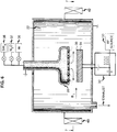
- FIG. 6 is a schematic sectional view of the chamber 22 of FIG. 5 used for depositing the first silicon dioxide layer 18 of FIG. 2.
- a wafer 30 is mounted on an electrode 31 connected through a matching network 32 to a radio-frequency source 33.
- a grounded electrode 35 opposite the wafer 30 constitutes a source of gas for forming an rf plasma between electrodes 35 and 31.
- the grounded electrode 35 is hollow and contains a plurality of apertures that permit the flow of injected gas as shown by the arrows.
- the gas is taken from a source of argon 36, a source of nitrogen oxide 37 and a source of silane 38. Appropriate valves and transmission lines permit a mixture of these gases to be directed into the region between the electrodes 35 and 31.
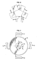
- coils 40 through 43 are located in quadrature around the chamber 22.
- the intended purpose of the chamber 22, as part of the "Precision 5000 System,” is to sputter etch material from wafers, rather than deposit the material on wafers.
- the coils produce a magnetic field through the wafer generally parallel with the upper surface of the wafer 30 and they promote sputter etching by increasing the density of impinging ions on the wafer surface.
- Coils 42 and 43 are connected together and, when current through them is at a maximum, they produce a magnetic field B1 shown in FIGs. 6 and 7.
- Interconnected coils 40 and 41 produce a magnetic field B2 when they carry current to the maximum.
- the current through coils 42 and 43 By directing current at a low alternation frequency through the coils, with the current through coils 42 and 43 being displaced ninety degrees from the current through coils 40 and 41, one can create a magnetic field of uniform strength B which rotates in a plane parallel to the upper surface of the wafer 30.
- the current is vied through the coils such that the magnetic field B remains of constant total strength and rotates with a frequency of one rotation for each two seconds although a frequency as high as one hundred rotations per second could be used.
- argon Prior to deposition, argon is introduced into the system and the rf power is applied so as to heat the wafer 30. Thereafter, gas from sources 37 and 38 are introduced.
- Nitrogen oxide, N2O constitutes a source of oxygen
- silane, SiH4 constitutes a source of silicon which are reacted to deposit silicon dioxide on the upper surface of the wafer in accordance with the principles of PECVD.
- these gases are chosen so as to enhance sputtering from the surface of wafer 30 as well as to constitute sources for deposition of silicon dioxide onto wafer 30.
- the wafer 30 is supported on an electrode 31 which is rf driven and is smaller in area than electrode 35.
- the total pressure within the chamber 22 is low and the rate of silicon dioxide deposition is relatively low. Together with the magnetic field, these choices of parameters tend to enhance sputtering.
- silicon dioxide 18 having an upper surface 45 that is generally V-shaped between successive conductors 13. This is accomplished because sputtering occurs predominantly at the corners of conductors 13, which results in a net thickness of deposition that is lowest at the corners. Thus, in effect, we deposit at a rate that is balanced with respect to the rate of removal by sputtering so as to give a minimum net deposition at the corners of conductors 13.
- the wafer is removed to transfer chamber 27 and then to chamber 23, which is shown schematically in FIG. 8.
- the upper electrode 47 rather than the lower electrode is driven by an rf source 48 (the matching network is not shown for purposes of brevity).
- the wafer 30 rests on a grounded electrode 49.
- gases are directed through electrode 47 toward the wafer 30, but different gas compositions are used.
- the silicon component of the silicon dioxide is obtained from gaseous tetraethoxysilane (TEOS) derived from a heated liquid source 51.
- TEOS gaseous tetraethoxysilane
- TEOS is commercially available as a liquid and a vaporized form is obtained by bubbling helium from a source 52 through the liquid TEOS and deriving vaporized molecules from the TEOS container as indicated schematically. Also included in the plasma atmosphere is pure oxygen gas from source 53. Various known valves and metering equipment are not shown for brevity.
- the lower electrode 49 is heated by a plurality of lamps 55 that direct light through a quartz window 56 so as to impinge on an aluminum oxide layer 57 of electrode 49. This heats the wafer to a temperature below the melting point of the metal conductors contained on its surface.
- the gas composition of the plasma atmosphere and the various other parameters are chosen so as to maximize the silicon dioxide deposition rate.
- this process yields a conformal coating 19 having an upper surface 59 that corresponds generally to the upper surface 45 of the silicon dioxide layer 18 of FIG. 2.
- the upper surface of silicon dioxide layer 19 is then planarized in a known manner to yield the silicon dioxide layer 19 of FIG. 4 upon which one may then deposit the second level of conductors 20.
- the silicon dioxide 19 may be ground to a horizontal level equal to the top level of conductors 13 using the top surface of the conductors as a "stop" to the grinding operation. Thereafter, another silicon dioxide layer is deposited in the chamber 22 of FIG. 6 to yield a silicon dioxide layer having a flat upper surface. As still another option, etching may be used to planarize the upper surface of deposited layer 19.
- the crux of the invention lies in depositing a first silicon dioxide layer 18 having the upper surface 45 generally as shown.
- the vertical walls are prevented from growing together by depositing the silicon dioxide 18 so as to have V-shaped upper surfaces between successive conductors which, in turn, requires a balance between removal of material by sputtering and deposition of silicon dioxide by PECVD.
- Table I below shows the parameters that were used in both chambers 22 and 23 for covering conductors having aspect ratios up to 1.7. The table also shows the parameters used in chamber 23 for increasing the deposition rate of the silicon dioxide.
- Table I demonstrates the radically different conditions for silicon dioxide deposition in chamber 22 with respect to that in chamber 23.
- A means angstrom units and sccm means standard cubic centimeters per minute.
- Many experiments have demonstrated to me that the desirable objective of depositing in chamber 22 is to maximize the sputtering rate, because the rate at which the silicon dioxide can be deposited is limited by the rate at which it must be sputtered away from the corners of the conductors; the time taken for the overall process is reduced by increasing both the sputtering and deposition rates in chamber 22.
- argon is used to increase the mass of impinging ions on the surface of the wafer.
- a much lower pressure is used in chamber 22 (between one and one hundred millitorr) than in chamber 23 (between about one and twenty torr).
- the electrode 31 of chamber 22 is made smaller than electrode 35 and is driven by the rf source 33 in order to maximize the energy of ion impingement on the wafer surface.
- the magnetic field greatly increases sputtering rate and therefore greatly improves the efficiency of chamber 22.
- One hundred thirty gauss was the highest magnetic field that could be obtained in the system used; it appear that this value should be significantly increased to speed up the overall process.
- Silane as the silicon source and N2O as the oxygen source further enhance the sputtering component.
- a high rf power in chamber 22 (i.e., power in excess of at least one hundred watts) is preferred to maximize sputtering and, in fact, the rf power and the magnetic field are perhaps the two most important parameters for increasing the sputtering component.
- TEOS, O2, and other alternative gases could be used in chamber 22, but the process window for good quality films is much narrower with these gases in chamber 22.
- chamber 23 one wishes to maximize the deposition rate and so TEOS and O2 are appropriate choices. By maximizing the sputtering rate in chamber 22, one minimizes the time needed to establish the configuration of FIG. 2.
- the deposition rate in chamber 23 is 125 angstroms per second and in chamber 22 the rate is only 700 angstroms per minute.
- the electrode 49 that supports wafer 30 is smaller than the electrode 47 and the electrode spacing is only 200 mils because there is no need for any sputtering component.
Abstract
Description
- This invention relates to methods and apparatus for depositing silicon dioxide and, more particularly, to methods for depositing silicon dioxide over conductors of an integrated circuit having a relatively high aspect ratio.
- The technology of integrated circuits has been characterized by a continuing increase in the density with which devices can be formed in a silicon semiconductor chip or substrate. The interconnection of such high density devices requires the formation on the chip surface of conductors that are extremely small and spaced closely together, and conductive patterns that overlap, or, in the terminology of the technology, are vertically spaced at different conductor levels. The use of two or more levels of conductors requires a deposition of a dependable insulation such as silicon dioxide on the lower or first level of conductors so that the overlying upper level or second level can be made without the risk of accidental short circuits or other conductive anomalies.
- A favored method for depositing silicon dioxide is known as plasma enhanced chemical vapor deposition (PECVD) in which a radio-frequency plasma contains a silicon component and an oxygen component. The plasma provides energy for enhancing the reaction required for silicon dioxide formation at temperatures below the melting point of the first level of conductors over which the deposition is made. It should be noted that other oxides such as silicon monoxide may be deposited by this process, but the predominant deposited material is silicon dioxide, which is the term that will be used herein. Also, deposition is on a "substrate," which may be part of the semiconductor, the metal conductors, or previously deposited or grown silicon dioxide.
- As circuit density increases, the ratio of the height of adjacent conductors to their separation distance, known as the aspect ratio of the structure, also increases. If the thickness of the deposited silicon dioxide is greater than half the separation between adjacent conductors, the silicon dioxide deposited on adjacent vertical walls of adjacent conductors is likely to meet and cause a discontinuity in the deposited silicon dioxide. If the top corner coverage is slightly greater than the coverage on the remainder of the vertical sidewalls, the corners may meet first, thus producing a void within the deposited silicon dioxide between adjacent conductors. This problem becomes more pressing as the aspect ratio increases.
- One solution to the problem is the use of electron cyclotron resonance (ECR) as described, for example, in the paper, "SiO₂ Planarization Technology with Biasing and Electron Cyclotron Resonance Plasma Deposition for Submicron Interconnections," Katsuyuki Machida et al., Journal of Vacuum Science Technology B4 (4), July/August 1986, pp. 818-821. In a chamber connected to the deposition chamber, the combination of an applied microwave frequency and magnetic field sets up a cyclotron resonance of ions which are directed into the deposition chamber and cause silicon dioxide to deposit. The addition of a wafer rf bias in the deposition chamber causes the silicon dioxide to sputter etch, resulting in deposition at different angles on the substrate, thereby to reduce the problem of voids caused by merging vertical walls. One problem with this approach is that it requires the design of new equipment, it is more difficult to maintain the standards of ultracleanliness required in chip manufacture, and the need for microwaves and a separate ECR chamber complicate and increase the cost of the apparatus for manufacture.
- The paper, " Sidewall-Tapered Oxide by Plasma-Enhanced Chemical Vapor Deposition," G. C. Smith et al., Journal of Electrochemical Society: Solid-State Science and Technology, Vol. 132, No. 11, November 1985, pp. 2721-2725, describes another approach in which sputtering is induced concurrently with silicon dioxide deposition. This leads to V-shaped sidewalls of the deposited silicon dioxide, rather than vertical sidewalls that merge to create voids. A problem with this approach is the relatively long time period required for depositing a useful layer of silicon dioxide over a conductor pattern having a relatively high aspect ratio.
- There is therefore a continuing need in industry for a method for depositing dependable layers of silicon dioxide over conductor patterns having high aspect ratios in a manner that is amenable to mass production, is consistent with cleanliness requirements, and which does not greatly increase the cost of manufacture.
- Equipment is available on the market for sputter etching a wafer in one chamber and then moving it to another chamber for silicon dioxide deposition. I have found that, with practical modifications, such equipment can expediently be used to deposit silicon dioxide over conductors having high aspect ratios. In the modified sputter etch chamber, an rf plasma is formed for depositing a layer of silicon dioxide. A magnetic field extends through the wafer and plasma, in a direction generally transverse to the rf field. Simultaneous sputter etching and deposition occurs which inhibits net deposition on the corners of the first level conductors; this results in a generally V-shaped surface to the deposited silicon dioxide between adjacent conductors. This could constitute the entire deposition, but preferably the substrate is removed and transferred to the conventional deposition chamber. Here, a generally conformal second layer of silicon dioxide is formed over the previously deposited layer but, because of the configuration of the first silicon dioxide layer, there can be no problems of voids or other discontinuities. Thereafter, the upper surface is planarized and the second level of conductors is deposited.
- The method which has been briefly described yields a reliable silicon dioxide insulation layer in a manner which is consistent with mass production and operation by workers of moderate skill. No problems of cleanliness are introduced because the equipment that is used is, for the most part, commercially available equipment that has been designed to meet modern standards of cleanliness. As will become clear from the detailed description, there is little added cost to the apparatus or method which is used in obtaining the silicon dioxide dielectric layers. These and other objects, features and benefits of the invention will be better understood from a consideration of the following detailed description taken in conjunction with the accompanying drawing.
-
- FIG. 1 is a schematic view of silicon dioxide deposited over metal conductors in accordance with the prior art;
- FIGs. 2, 3 and 4 are schematic views illustrating successive steps of silicon dioxide dielectric formation in accordance with an illustrative embodiment of the invention;
- FIG. 5 is a schematic view of certain commercially available equipment that can be modified to be used in accordance with the invention;
- FIG. 6 is a schematic view of one modified reactor chamber in chamber apparatus of FIG. 5;
- FIG. 7 is a view taken along line 7-7 of FIG. 6; and
- FIG. 8 is a schematic view of another reactor chamber of the apparatus of FIG. 5.
- Referring now to FIG. 1, there is illustrated schematically the prior art deposition of silicon dioxide 11 on a
substrate 12, which creates the problem with which the invention is concerned. Located on the top surface of thesubstrate 12 areconductors 13, which illustratively constitute the first conductor level of an integrated circuit. The aspect ratio of the conductors is defined as the ratio of the height of thevertical sidewalls 14 of the conductors to the separation distance of adjacent vertical sidewalls of adjacent conductors. With conventional conformal deposition, a high aspect ratio results in the silicon dioxide on adjacent vertical walls growing together. The corners of the deposited silicon dioxide are likely to meet first, which results invoids 15 in the deposited oxide layer. Even if voids are not formed,discontinuities 16 are created, which adversely affect the etch characteristics and insulation characteristics of the silicon dioxide layer. One can appreciate that as the aspect ratio increases, the problems accompanying conformal silicon dioxide deposition generally increase. - Referring to FIG. 2, in accordance with the invention, the silicon dioxide is formed in two steps. First, a first
silicon dioxide layer 18 is formed, which has generally a V-shaped configuration betweenadjacent conductors 13 as shown. Then, as shown in FIG. 3, a secondsilicon dioxide layer 19 is formed over the first silicon dioxide layer, which is generally conformal and therefore has a succession of V-shapes in its upper surface as shown. FIG. 4 shows the silicon dioxide layer planarized so as to permit the formation ofconductors 20 on its upper surface, which constitutes the second conductor level of the integrated circuit device being made. - An important aspect of the inventive method is that it can be practiced through the use of commercially available chemical vapor deposition (CVD) equipment. Specifically, FIG. 5 illustrates schematically apparatus known as the "Precision 5000 System," commercially available from the Applied Materials Company of Santa Clara, California, which may be used for the practice of the invention. This system includes separate chambers 22-25 interconnected by a
central transfer chamber 27. Wafers are introduced into aload lock chamber 26 and are transferred among various chambers by a robot arm contained in atransfer chamber 27. These individual chambers can be used for different operations on semiconductor wafers while maintaining high standards of cleanliness and avoiding cross contamination from one chamber to the other. By using separate chambers to depositlayers 18 and 19 (of FIG. 3), one can optimize the parameters to obtain the highest possible overall deposition rate, or, in other words, to reduce as much as possible the overall time required for the entire process. - FIG. 6 is a schematic sectional view of the
chamber 22 of FIG. 5 used for depositing the firstsilicon dioxide layer 18 of FIG. 2. Awafer 30 is mounted on anelectrode 31 connected through amatching network 32 to a radio-frequency source 33. A groundedelectrode 35 opposite thewafer 30 constitutes a source of gas for forming an rf plasma betweenelectrodes electrode 35 is hollow and contains a plurality of apertures that permit the flow of injected gas as shown by the arrows. The gas is taken from a source ofargon 36, a source of nitrogen oxide 37 and a source ofsilane 38. Appropriate valves and transmission lines permit a mixture of these gases to be directed into the region between theelectrodes - As can be seen in FIG. 7, four
coils 40 through 43 are located in quadrature around thechamber 22. The intended purpose of thechamber 22, as part of the "Precision 5000 System," is to sputter etch material from wafers, rather than deposit the material on wafers. To this end, the coils produce a magnetic field through the wafer generally parallel with the upper surface of thewafer 30 and they promote sputter etching by increasing the density of impinging ions on the wafer surface.Coils Interconnected coils coils coils wafer 30. Preferably, the current is vied through the coils such that the magnetic field B remains of constant total strength and rotates with a frequency of one rotation for each two seconds although a frequency as high as one hundred rotations per second could be used. - Prior to deposition, argon is introduced into the system and the rf power is applied so as to heat the
wafer 30. Thereafter, gas fromsources 37 and 38 are introduced. Nitrogen oxide, N₂O, constitutes a source of oxygen, and silane, SiH₄, constitutes a source of silicon which are reacted to deposit silicon dioxide on the upper surface of the wafer in accordance with the principles of PECVD. As will be explained later, these gases are chosen so as to enhance sputtering from the surface ofwafer 30 as well as to constitute sources for deposition of silicon dioxide ontowafer 30. Thewafer 30 is supported on anelectrode 31 which is rf driven and is smaller in area thanelectrode 35. The total pressure within thechamber 22 is low and the rate of silicon dioxide deposition is relatively low. Together with the magnetic field, these choices of parameters tend to enhance sputtering. - Referring again to FIG. 2, it is desired in the apparatus of FIGs. 6 and 7 to deposit
silicon dioxide 18 having anupper surface 45 that is generally V-shaped betweensuccessive conductors 13. This is accomplished because sputtering occurs predominantly at the corners ofconductors 13, which results in a net thickness of deposition that is lowest at the corners. Thus, in effect, we deposit at a rate that is balanced with respect to the rate of removal by sputtering so as to give a minimum net deposition at the corners ofconductors 13. I have found that using parameters designed to give a sputtering rate of three hundred angstroms per minute and a silicon dioxide deposition rate of one thousand angstroms per minute will yield a net deposition rate of seven hundred angstroms per minute and will yield theupper surface 45 shown in FIG. 2. The rotation of the magnetic field B enhances uniformity of deposition. - Referring again to FIG. 5, after completion of the silicon dioxide deposition in
chamber 22, the wafer is removed to transferchamber 27 and then tochamber 23, which is shown schematically in FIG. 8. Inchamber 23, theupper electrode 47, rather than the lower electrode is driven by an rf source 48 (the matching network is not shown for purposes of brevity). Thewafer 30 rests on a groundedelectrode 49. As before, gases are directed throughelectrode 47 toward thewafer 30, but different gas compositions are used. The silicon component of the silicon dioxide is obtained from gaseous tetraethoxysilane (TEOS) derived from a heatedliquid source 51. Typically, TEOS is commercially available as a liquid and a vaporized form is obtained by bubbling helium from asource 52 through the liquid TEOS and deriving vaporized molecules from the TEOS container as indicated schematically. Also included in the plasma atmosphere is pure oxygen gas fromsource 53. Various known valves and metering equipment are not shown for brevity. - The
lower electrode 49 is heated by a plurality oflamps 55 that direct light through aquartz window 56 so as to impinge on analuminum oxide layer 57 ofelectrode 49. This heats the wafer to a temperature below the melting point of the metal conductors contained on its surface. - In the configuration of
chamber 23, the gas composition of the plasma atmosphere and the various other parameters are chosen so as to maximize the silicon dioxide deposition rate. Referring to FIG. 3, this process yields aconformal coating 19 having anupper surface 59 that corresponds generally to theupper surface 45 of thesilicon dioxide layer 18 of FIG. 2. One can appreciate that with the silicon dioxide depositing at a generally equal rate on all surfaces, there is not likely to be a problem of adjacent sidewalls growing together with consequent formation of voids as was described with reference to FIG. 1. The upper surface ofsilicon dioxide layer 19 is then planarized in a known manner to yield thesilicon dioxide layer 19 of FIG. 4 upon which one may then deposit the second level ofconductors 20. Alternatively, thesilicon dioxide 19 may be ground to a horizontal level equal to the top level ofconductors 13 using the top surface of the conductors as a "stop" to the grinding operation. Thereafter, another silicon dioxide layer is deposited in thechamber 22 of FIG. 6 to yield a silicon dioxide layer having a flat upper surface. As still another option, etching may be used to planarize the upper surface of depositedlayer 19. - Referring again to FIG. 2, it can be appreciated that the crux of the invention lies in depositing a first
silicon dioxide layer 18 having theupper surface 45 generally as shown. The vertical walls are prevented from growing together by depositing thesilicon dioxide 18 so as to have V-shaped upper surfaces between successive conductors which, in turn, requires a balance between removal of material by sputtering and deposition of silicon dioxide by PECVD. Table I below shows the parameters that were used in bothchambers chamber 23 for increasing the deposition rate of the silicon dioxide.
- Table I demonstrates the radically different conditions for silicon dioxide deposition in
chamber 22 with respect to that inchamber 23. In the table, A means angstrom units and sccm means standard cubic centimeters per minute. Many experiments have demonstrated to me that the desirable objective of depositing inchamber 22 is to maximize the sputtering rate, because the rate at which the silicon dioxide can be deposited is limited by the rate at which it must be sputtered away from the corners of the conductors; the time taken for the overall process is reduced by increasing both the sputtering and deposition rates inchamber 22. Thus, to maximize sputtering rate, argon is used to increase the mass of impinging ions on the surface of the wafer. A much lower pressure is used in chamber 22 (between one and one hundred millitorr) than in chamber 23 (between about one and twenty torr). Theelectrode 31 ofchamber 22 is made smaller thanelectrode 35 and is driven by therf source 33 in order to maximize the energy of ion impingement on the wafer surface. The magnetic field greatly increases sputtering rate and therefore greatly improves the efficiency ofchamber 22. One hundred thirty gauss was the highest magnetic field that could be obtained in the system used; it appear that this value should be significantly increased to speed up the overall process. Silane as the silicon source and N₂O as the oxygen source further enhance the sputtering component. A high rf power in chamber 22 (i.e., power in excess of at least one hundred watts) is preferred to maximize sputtering and, in fact, the rf power and the magnetic field are perhaps the two most important parameters for increasing the sputtering component. Of course, TEOS, O₂, and other alternative gases could be used inchamber 22, but the process window for good quality films is much narrower with these gases inchamber 22. Inchamber 23, one wishes to maximize the deposition rate and so TEOS and O₂ are appropriate choices. By maximizing the sputtering rate inchamber 22, one minimizes the time needed to establish the configuration of FIG. 2. Thus, in the embodiment described, the deposition rate inchamber 23 is 125 angstroms per second and inchamber 22 the rate is only 700 angstroms per minute. In thechamber 23, no effort is made to make theelectrode 49 that supportswafer 30 smaller than theelectrode 47 and the electrode spacing is only 200 mils because there is no need for any sputtering component. - In the "Precision 5000 System" that was used, a pair of quartz rings and a graphite ring that surrounded
electrode 31 ofchamber 22 were removed. Other minor structural changes were made, but essentially full advantage was taken of the commercially available system for processing semiconductor wafers with a high throughput. The diameter ofelectrode 31 was adjusted to be approximately equal to that of the wafer 30 (six inches). The purpose of these changes was to make as uniform as possible the plasma distribution over the upper surface of the wafer, and as mentioned before it appears that substitute coils should be used to give a higher rotating magnetic field. - The various parameters which are described merely illustrate in one embodiment the optimum choices for balance sputtering with deposition. Various other gases could be used in which case the parameters should be adjusted accordingly. Ony a single chamber could be used for making both depositions, but in that case more compromises in apparatus structure would have to be made. It is not essential that the magnetic field rotate if one can tolerate non-uniform deposition and density. Various other embodiments and modifications may be made by those skilled in the art without departing from the spirit and scope of the invention.
Claims (10)
- A method for making an integrated circuit device comprising the steps of depositing a first layer (18) of silicon dioxide on a substrate (12) surface by exposing the substrate surface to an rf plasma in an atmosphere including silicon and oxygen components, characterized by:
forming a magnetic field (B) that extends through the substrate and through the plasma contiguous to the surface in a direction substantially parallel to the surface;
the rf plasma is formed by subjecting the atmosphere to rf power in excess of one hundred watts;
and the plasma contains an inert gas component, the magnetic field, rf power and inert gas cooperating to cause sputtering preferentially at discontinuities of the substrate.. - The method of claim 1 further characterized in that:
during deposition, the magnetic field is caused to rotate in a plane substantially parallel to the substrate surface. - The method of claim 1 or 2 further characterized in that:
the substrate has a generally planar configuration and is supported such that its exposed surface is a relatively large-area surface of the substrate and is located in a substantially horizontal plane;
and the substrate surface contains a plurality of relatively closely spaced conductive elements (13) having adjacent vertical wall portions (14), whereby the electric and magnetic fields cause a sputtering phenomenon primarily at exposed corners of the conductive elements. - The method of claim 3 further characterized in that:
the magnetic field has a value at the substrate surface of more than about one hundred gauss. - The method of claim 1, 2 or 4 further characterized in that:
the magnetic field is defined by a magnetic field vector of substantially constant value that rotates at a frequency of between about 0.5 and one hundred rotations per second. - The method of claim 1, 2 or 5 further characterized in that:
a second layer (19) of silicon dioxide is deposited on the first layer by exposing the substrate surface to an rf plasma in an atmosphere containing silicon and oxygen components, but without a magnetic field. - The method of claim 6 further characterized in that:
during formation of the first layer, the substrate is supported on an rf excited electrode, and during formation of the second layer, the substrate is supported on a grounded electrode. - The method of claim 6 or 7 further characterized in that:
during formation of the first layer, the atmosphere contains an inert gas component, and during formation of the second layer, the atmosphere contains substantially no inert gas component and the total gas pressure of the atmosphere is much higher during formation of the second layer than during formation of the first layer. - The method of claim 6, 7 or 8 further characterized in that:
during formation of the first layer, the silicon component in the atmosphere comprises silane and the oxygen component comprises nitrogen oxide, and, during formation of the second layer, the silicon component comprises tetraethoxysilane and the oxygen component comprises pure oxygen. - The method of claim 6, 8 or 9 further comprising the step of:
planarizing an upper surface of the deposited second silicon dioxide;
and forming a second conductive pattern on the planarized second silicon dioxide surface.
Applications Claiming Priority (2)
| Application Number | Priority Date | Filing Date | Title |
|---|---|---|---|
| US07/584,986 US5089442A (en) | 1990-09-20 | 1990-09-20 | Silicon dioxide deposition method using a magnetic field and both sputter deposition and plasma-enhanced cvd |
| US584986 | 1990-09-20 |
Publications (3)
| Publication Number | Publication Date |
|---|---|
| EP0478174A2 true EP0478174A2 (en) | 1992-04-01 |
| EP0478174A3 EP0478174A3 (en) | 1992-04-15 |
| EP0478174B1 EP0478174B1 (en) | 1998-07-29 |
Family
ID=24339594
Family Applications (1)
| Application Number | Title | Priority Date | Filing Date |
|---|---|---|---|
| EP91308268A Expired - Lifetime EP0478174B1 (en) | 1990-09-20 | 1991-09-11 | Silicon dioxide deposition method |
Country Status (5)
| Country | Link |
|---|---|
| US (1) | US5089442A (en) |
| EP (1) | EP0478174B1 (en) |
| JP (1) | JPH07101688B2 (en) |
| DE (1) | DE69129885T2 (en) |
| SG (1) | SG43945A1 (en) |
Cited By (4)
| Publication number | Priority date | Publication date | Assignee | Title |
|---|---|---|---|---|
| EP0574100A2 (en) * | 1992-04-16 | 1993-12-15 | Mitsubishi Jukogyo Kabushiki Kaisha | Plasma CVD method and apparatus therefor |
| EP0622474A1 (en) * | 1993-04-29 | 1994-11-02 | L'air Liquide, Societe Anonyme Pour L'etude Et L'exploitation Des Procedes Georges Claude | Continuous process for making a silica coating on a solid substrate |
| WO1999043026A1 (en) * | 1998-02-19 | 1999-08-26 | Applied Materials, Inc. | Method and apparatus for improving gap-fill capability using chemical and physical etchbacks |
| US6821577B2 (en) | 1998-03-20 | 2004-11-23 | Applied Materials, Inc. | Staggered in-situ deposition and etching of a dielectric layer for HDP CVD |
Families Citing this family (231)
| Publication number | Priority date | Publication date | Assignee | Title |
|---|---|---|---|---|
| JP3362397B2 (en) * | 1991-03-28 | 2003-01-07 | ソニー株式会社 | Manufacturing method of electronic device including polishing step by polishing |
| US5470772A (en) * | 1991-11-06 | 1995-11-28 | Intel Corporation | Silicidation method for contactless EPROM related devices |
| JPH05243402A (en) * | 1992-03-03 | 1993-09-21 | Nec Corp | Manufacture of semiconductor device |
| US5360769A (en) * | 1992-12-17 | 1994-11-01 | Micron Semiconductor, Inc. | Method for fabricating hybrid oxides for thinner gate devices |
| US5416048A (en) * | 1993-04-16 | 1995-05-16 | Micron Semiconductor, Inc. | Method to slope conductor profile prior to dielectric deposition to improve dielectric step-coverage |
| US5503882A (en) * | 1994-04-18 | 1996-04-02 | Advanced Micro Devices, Inc. | Method for planarizing an integrated circuit topography |
| US5494854A (en) * | 1994-08-17 | 1996-02-27 | Texas Instruments Incorporated | Enhancement in throughput and planarity during CMP using a dielectric stack containing HDP-SiO2 films |
| US5686356A (en) | 1994-09-30 | 1997-11-11 | Texas Instruments Incorporated | Conductor reticulation for improved device planarity |
| KR0159016B1 (en) * | 1995-06-28 | 1999-02-01 | 김주용 | Method of manufacturing insulation film inter metal wire in a semiconductor device |
| JP2674585B2 (en) * | 1995-09-28 | 1997-11-12 | 日本電気株式会社 | Method for manufacturing semiconductor device |
| US5861342A (en) * | 1995-12-26 | 1999-01-19 | Vlsi Technology, Inc. | Optimized structures for dummy fill mask design |
| DE69623651T2 (en) * | 1995-12-27 | 2003-04-24 | Lam Res Corp | METHOD FOR FILLING TRENCHES ON A SEMICONDUCTOR DISC |
| US6191026B1 (en) | 1996-01-09 | 2001-02-20 | Applied Materials, Inc. | Method for submicron gap filling on a semiconductor substrate |
| US5639697A (en) * | 1996-01-30 | 1997-06-17 | Vlsi Technology, Inc. | Dummy underlayers for improvement in removal rate consistency during chemical mechanical polishing |
| US5783488A (en) * | 1996-01-31 | 1998-07-21 | Vlsi Technology, Inc. | Optimized underlayer structures for maintaining chemical mechanical polishing removal rates |
| US6106678A (en) * | 1996-03-29 | 2000-08-22 | Lam Research Corporation | Method of high density plasma CVD gap-filling |
| US6827824B1 (en) | 1996-04-12 | 2004-12-07 | Micron Technology, Inc. | Enhanced collimated deposition |
| US5888901A (en) * | 1996-08-05 | 1999-03-30 | Motorola, Inc. | Multilevel interconnection and method for making |
| US6534409B1 (en) | 1996-12-04 | 2003-03-18 | Micron Technology, Inc. | Silicon oxide co-deposition/etching process |
| US6184158B1 (en) * | 1996-12-23 | 2001-02-06 | Lam Research Corporation | Inductively coupled plasma CVD |
| US5854125A (en) * | 1997-02-24 | 1998-12-29 | Vlsi Technology, Inc. | Dummy fill patterns to improve interconnect planarity |
| US6136685A (en) * | 1997-06-03 | 2000-10-24 | Applied Materials, Inc. | High deposition rate recipe for low dielectric constant films |
| US6150072A (en) * | 1997-08-22 | 2000-11-21 | Siemens Microelectronics, Inc. | Method of manufacturing a shallow trench isolation structure for a semiconductor device |
| US6176983B1 (en) * | 1997-09-03 | 2001-01-23 | Vlsi Technology, Inc. | Methods of forming a semiconductor device |
| US6150285A (en) * | 1998-06-17 | 2000-11-21 | Advanced Micro Devices, Inc. | Method for simultaneous deposition and sputtering of TEOS |
| KR100319185B1 (en) * | 1998-07-31 | 2002-01-04 | 윤종용 | Method for forming dielectric layer |
| US6384466B1 (en) * | 1998-08-27 | 2002-05-07 | Micron Technology, Inc. | Multi-layer dielectric and method of forming same |
| US6225210B1 (en) * | 1998-12-09 | 2001-05-01 | Advanced Micro Devices, Inc. | High density capping layers with improved adhesion to copper interconnects |
| US6927160B1 (en) | 1999-06-09 | 2005-08-09 | National Semiconductor Corporation | Fabrication of copper-containing region such as electrical interconnect |
| US7381638B1 (en) | 1999-06-09 | 2008-06-03 | National Semiconductor Corporation | Fabrication technique using sputter etch and vacuum transfer |
| US6093634A (en) * | 1999-07-26 | 2000-07-25 | United Microelectronics Corp. | Method of forming a dielectric layer on a semiconductor wafer |
| US6319796B1 (en) | 1999-08-18 | 2001-11-20 | Vlsi Technology, Inc. | Manufacture of an integrated circuit isolation structure |
| US6503843B1 (en) | 1999-09-21 | 2003-01-07 | Applied Materials, Inc. | Multistep chamber cleaning and film deposition process using a remote plasma that also enhances film gap fill |
| US6335288B1 (en) | 2000-08-24 | 2002-01-01 | Applied Materials, Inc. | Gas chemistry cycling to achieve high aspect ratio gapfill with HDP-CVD |
| TW479315B (en) | 2000-10-31 | 2002-03-11 | Applied Materials Inc | Continuous depostiton process |
| TW478099B (en) | 2000-11-03 | 2002-03-01 | Applied Materials Inc | Shallow trench isolation manufacture method |
| GB0100151D0 (en) * | 2001-01-04 | 2001-02-14 | Trikon Holdings Ltd | Methods of sputtering |
| US6447651B1 (en) | 2001-03-07 | 2002-09-10 | Applied Materials, Inc. | High-permeability magnetic shield for improved process uniformity in nonmagnetized plasma process chambers |
| US6740601B2 (en) * | 2001-05-11 | 2004-05-25 | Applied Materials Inc. | HDP-CVD deposition process for filling high aspect ratio gaps |
| US6596653B2 (en) * | 2001-05-11 | 2003-07-22 | Applied Materials, Inc. | Hydrogen assisted undoped silicon oxide deposition process for HDP-CVD |
| US7115516B2 (en) * | 2001-10-09 | 2006-10-03 | Applied Materials, Inc. | Method of depositing a material layer |
| US6869880B2 (en) * | 2002-01-24 | 2005-03-22 | Applied Materials, Inc. | In situ application of etch back for improved deposition into high-aspect-ratio features |
| US6908862B2 (en) * | 2002-05-03 | 2005-06-21 | Applied Materials, Inc. | HDP-CVD dep/etch/dep process for improved deposition into high aspect ratio features |
| DE10228771B4 (en) * | 2002-06-27 | 2008-02-14 | Infineon Technologies Ag | Process for planarization with definable Planarisierungslänge in semiconductor integrated circuits and such a semiconductor integrated circuit |
| AU2003270496A1 (en) * | 2002-09-09 | 2004-03-29 | Oster Magnetics, Inc. | Apparatus for manipulating magnetic fields |
| US20070212850A1 (en) * | 2002-09-19 | 2007-09-13 | Applied Materials, Inc. | Gap-fill depositions in the formation of silicon containing dielectric materials |
| US7335609B2 (en) * | 2004-08-27 | 2008-02-26 | Applied Materials, Inc. | Gap-fill depositions introducing hydroxyl-containing precursors in the formation of silicon containing dielectric materials |
| US7141483B2 (en) * | 2002-09-19 | 2006-11-28 | Applied Materials, Inc. | Nitrous oxide anneal of TEOS/ozone CVD for improved gapfill |
| US7431967B2 (en) * | 2002-09-19 | 2008-10-07 | Applied Materials, Inc. | Limited thermal budget formation of PMD layers |
| US7456116B2 (en) * | 2002-09-19 | 2008-11-25 | Applied Materials, Inc. | Gap-fill depositions in the formation of silicon containing dielectric materials |
| US6802944B2 (en) * | 2002-10-23 | 2004-10-12 | Applied Materials, Inc. | High density plasma CVD process for gapfill into high aspect ratio features |
| US7628897B2 (en) * | 2002-10-23 | 2009-12-08 | Applied Materials, Inc. | Reactive ion etching for semiconductor device feature topography modification |
| US6808748B2 (en) * | 2003-01-23 | 2004-10-26 | Applied Materials, Inc. | Hydrogen assisted HDP-CVD deposition process for aggressive gap-fill technology |
| US7081414B2 (en) * | 2003-05-23 | 2006-07-25 | Applied Materials, Inc. | Deposition-selective etch-deposition process for dielectric film gapfill |
| US6958112B2 (en) * | 2003-05-27 | 2005-10-25 | Applied Materials, Inc. | Methods and systems for high-aspect-ratio gapfill using atomic-oxygen generation |
| US7205240B2 (en) | 2003-06-04 | 2007-04-17 | Applied Materials, Inc. | HDP-CVD multistep gapfill process |
| US6903031B2 (en) * | 2003-09-03 | 2005-06-07 | Applied Materials, Inc. | In-situ-etch-assisted HDP deposition using SiF4 and hydrogen |
| US20060061443A1 (en) * | 2003-10-14 | 2006-03-23 | Oster Magnetics, Inc. | Apparatus for manipulating magnetic fields |
| US20050136684A1 (en) * | 2003-12-23 | 2005-06-23 | Applied Materials, Inc. | Gap-fill techniques |
| US20050260356A1 (en) * | 2004-05-18 | 2005-11-24 | Applied Materials, Inc. | Microcontamination abatement in semiconductor processing |
| US7229931B2 (en) * | 2004-06-16 | 2007-06-12 | Applied Materials, Inc. | Oxygen plasma treatment for enhanced HDP-CVD gapfill |
| US7183227B1 (en) | 2004-07-01 | 2007-02-27 | Applied Materials, Inc. | Use of enhanced turbomolecular pump for gapfill deposition using high flows of low-mass fluent gas |
| US20070212847A1 (en) * | 2004-08-04 | 2007-09-13 | Applied Materials, Inc. | Multi-step anneal of thin films for film densification and improved gap-fill |
| US7642171B2 (en) * | 2004-08-04 | 2010-01-05 | Applied Materials, Inc. | Multi-step anneal of thin films for film densification and improved gap-fill |
| US7087536B2 (en) * | 2004-09-01 | 2006-08-08 | Applied Materials | Silicon oxide gapfill deposition using liquid precursors |
| JP2006165386A (en) * | 2004-12-09 | 2006-06-22 | Showa Shell Sekiyu Kk | Cis system thin film solar cell and method for manufacturing the same |
| US20060154494A1 (en) * | 2005-01-08 | 2006-07-13 | Applied Materials, Inc., A Delaware Corporation | High-throughput HDP-CVD processes for advanced gapfill applications |
| US7329586B2 (en) * | 2005-06-24 | 2008-02-12 | Applied Materials, Inc. | Gapfill using deposition-etch sequence |
| KR100675895B1 (en) * | 2005-06-29 | 2007-02-02 | 주식회사 하이닉스반도체 | Metal interconnection of semiconductor device and method of fabricating the same |
| US7524750B2 (en) | 2006-04-17 | 2009-04-28 | Applied Materials, Inc. | Integrated process modulation (IPM) a novel solution for gapfill with HDP-CVD |
| KR100752190B1 (en) * | 2006-09-04 | 2007-08-27 | 동부일렉트로닉스 주식회사 | Method for gapfilling in semiconductor device |
| US7939422B2 (en) * | 2006-12-07 | 2011-05-10 | Applied Materials, Inc. | Methods of thin film process |
| US20080142483A1 (en) * | 2006-12-07 | 2008-06-19 | Applied Materials, Inc. | Multi-step dep-etch-dep high density plasma chemical vapor deposition processes for dielectric gapfills |
| US7678715B2 (en) * | 2007-12-21 | 2010-03-16 | Applied Materials, Inc. | Low wet etch rate silicon nitride film |
| US8869741B2 (en) * | 2008-12-19 | 2014-10-28 | Lam Research Corporation | Methods and apparatus for dual confinement and ultra-high pressure in an adjustable gap plasma chamber |
| US9324576B2 (en) | 2010-05-27 | 2016-04-26 | Applied Materials, Inc. | Selective etch for silicon films |
| US8741778B2 (en) | 2010-12-14 | 2014-06-03 | Applied Materials, Inc. | Uniform dry etch in two stages |
| US10283321B2 (en) | 2011-01-18 | 2019-05-07 | Applied Materials, Inc. | Semiconductor processing system and methods using capacitively coupled plasma |
| US8771539B2 (en) | 2011-02-22 | 2014-07-08 | Applied Materials, Inc. | Remotely-excited fluorine and water vapor etch |
| US9064815B2 (en) | 2011-03-14 | 2015-06-23 | Applied Materials, Inc. | Methods for etch of metal and metal-oxide films |
| US8999856B2 (en) | 2011-03-14 | 2015-04-07 | Applied Materials, Inc. | Methods for etch of sin films |
| US8497211B2 (en) | 2011-06-24 | 2013-07-30 | Applied Materials, Inc. | Integrated process modulation for PSG gapfill |
| JP2013026599A (en) * | 2011-07-26 | 2013-02-04 | Elpida Memory Inc | Manufacturing method of semiconductor device |
| US8771536B2 (en) | 2011-08-01 | 2014-07-08 | Applied Materials, Inc. | Dry-etch for silicon-and-carbon-containing films |
| US8679982B2 (en) | 2011-08-26 | 2014-03-25 | Applied Materials, Inc. | Selective suppression of dry-etch rate of materials containing both silicon and oxygen |
| US8679983B2 (en) | 2011-09-01 | 2014-03-25 | Applied Materials, Inc. | Selective suppression of dry-etch rate of materials containing both silicon and nitrogen |
| US8927390B2 (en) | 2011-09-26 | 2015-01-06 | Applied Materials, Inc. | Intrench profile |
| US8808563B2 (en) | 2011-10-07 | 2014-08-19 | Applied Materials, Inc. | Selective etch of silicon by way of metastable hydrogen termination |
| WO2013070436A1 (en) | 2011-11-08 | 2013-05-16 | Applied Materials, Inc. | Methods of reducing substrate dislocation during gapfill processing |
| US9267739B2 (en) | 2012-07-18 | 2016-02-23 | Applied Materials, Inc. | Pedestal with multi-zone temperature control and multiple purge capabilities |
| US9373517B2 (en) | 2012-08-02 | 2016-06-21 | Applied Materials, Inc. | Semiconductor processing with DC assisted RF power for improved control |
| US9034770B2 (en) | 2012-09-17 | 2015-05-19 | Applied Materials, Inc. | Differential silicon oxide etch |
| US9023734B2 (en) | 2012-09-18 | 2015-05-05 | Applied Materials, Inc. | Radical-component oxide etch |
| US9390937B2 (en) | 2012-09-20 | 2016-07-12 | Applied Materials, Inc. | Silicon-carbon-nitride selective etch |
| US9132436B2 (en) | 2012-09-21 | 2015-09-15 | Applied Materials, Inc. | Chemical control features in wafer process equipment |
| US8765574B2 (en) | 2012-11-09 | 2014-07-01 | Applied Materials, Inc. | Dry etch process |
| US8969212B2 (en) | 2012-11-20 | 2015-03-03 | Applied Materials, Inc. | Dry-etch selectivity |
| US8980763B2 (en) | 2012-11-30 | 2015-03-17 | Applied Materials, Inc. | Dry-etch for selective tungsten removal |
| US9064816B2 (en) | 2012-11-30 | 2015-06-23 | Applied Materials, Inc. | Dry-etch for selective oxidation removal |
| US9111877B2 (en) | 2012-12-18 | 2015-08-18 | Applied Materials, Inc. | Non-local plasma oxide etch |
| US8921234B2 (en) | 2012-12-21 | 2014-12-30 | Applied Materials, Inc. | Selective titanium nitride etching |
| US9018108B2 (en) | 2013-01-25 | 2015-04-28 | Applied Materials, Inc. | Low shrinkage dielectric films |
| US10256079B2 (en) | 2013-02-08 | 2019-04-09 | Applied Materials, Inc. | Semiconductor processing systems having multiple plasma configurations |
| US9362130B2 (en) | 2013-03-01 | 2016-06-07 | Applied Materials, Inc. | Enhanced etching processes using remote plasma sources |
| US9040422B2 (en) | 2013-03-05 | 2015-05-26 | Applied Materials, Inc. | Selective titanium nitride removal |
| US8801952B1 (en) | 2013-03-07 | 2014-08-12 | Applied Materials, Inc. | Conformal oxide dry etch |
| US10170282B2 (en) | 2013-03-08 | 2019-01-01 | Applied Materials, Inc. | Insulated semiconductor faceplate designs |
| US20140271097A1 (en) | 2013-03-15 | 2014-09-18 | Applied Materials, Inc. | Processing systems and methods for halide scavenging |
| US8895449B1 (en) | 2013-05-16 | 2014-11-25 | Applied Materials, Inc. | Delicate dry clean |
| US9114438B2 (en) | 2013-05-21 | 2015-08-25 | Applied Materials, Inc. | Copper residue chamber clean |
| US9493879B2 (en) | 2013-07-12 | 2016-11-15 | Applied Materials, Inc. | Selective sputtering for pattern transfer |
| US9773648B2 (en) | 2013-08-30 | 2017-09-26 | Applied Materials, Inc. | Dual discharge modes operation for remote plasma |
| US8956980B1 (en) | 2013-09-16 | 2015-02-17 | Applied Materials, Inc. | Selective etch of silicon nitride |
| US8951429B1 (en) | 2013-10-29 | 2015-02-10 | Applied Materials, Inc. | Tungsten oxide processing |
| US9576809B2 (en) | 2013-11-04 | 2017-02-21 | Applied Materials, Inc. | Etch suppression with germanium |
| US9236265B2 (en) | 2013-11-04 | 2016-01-12 | Applied Materials, Inc. | Silicon germanium processing |
| US9520303B2 (en) | 2013-11-12 | 2016-12-13 | Applied Materials, Inc. | Aluminum selective etch |
| US9245762B2 (en) | 2013-12-02 | 2016-01-26 | Applied Materials, Inc. | Procedure for etch rate consistency |
| US9117855B2 (en) | 2013-12-04 | 2015-08-25 | Applied Materials, Inc. | Polarity control for remote plasma |
| US9263278B2 (en) | 2013-12-17 | 2016-02-16 | Applied Materials, Inc. | Dopant etch selectivity control |
| US9287095B2 (en) | 2013-12-17 | 2016-03-15 | Applied Materials, Inc. | Semiconductor system assemblies and methods of operation |
| US9190293B2 (en) | 2013-12-18 | 2015-11-17 | Applied Materials, Inc. | Even tungsten etch for high aspect ratio trenches |
| US9287134B2 (en) | 2014-01-17 | 2016-03-15 | Applied Materials, Inc. | Titanium oxide etch |
| US9293568B2 (en) | 2014-01-27 | 2016-03-22 | Applied Materials, Inc. | Method of fin patterning |
| US9396989B2 (en) | 2014-01-27 | 2016-07-19 | Applied Materials, Inc. | Air gaps between copper lines |
| US9385028B2 (en) | 2014-02-03 | 2016-07-05 | Applied Materials, Inc. | Air gap process |
| US9499898B2 (en) | 2014-03-03 | 2016-11-22 | Applied Materials, Inc. | Layered thin film heater and method of fabrication |
| US9299575B2 (en) | 2014-03-17 | 2016-03-29 | Applied Materials, Inc. | Gas-phase tungsten etch |
| US9299537B2 (en) | 2014-03-20 | 2016-03-29 | Applied Materials, Inc. | Radial waveguide systems and methods for post-match control of microwaves |
| US9299538B2 (en) | 2014-03-20 | 2016-03-29 | Applied Materials, Inc. | Radial waveguide systems and methods for post-match control of microwaves |
| US9136273B1 (en) | 2014-03-21 | 2015-09-15 | Applied Materials, Inc. | Flash gate air gap |
| US9903020B2 (en) | 2014-03-31 | 2018-02-27 | Applied Materials, Inc. | Generation of compact alumina passivation layers on aluminum plasma equipment components |
| US9269590B2 (en) | 2014-04-07 | 2016-02-23 | Applied Materials, Inc. | Spacer formation |
| US9309598B2 (en) | 2014-05-28 | 2016-04-12 | Applied Materials, Inc. | Oxide and metal removal |
| US9847289B2 (en) | 2014-05-30 | 2017-12-19 | Applied Materials, Inc. | Protective via cap for improved interconnect performance |
| US9378969B2 (en) | 2014-06-19 | 2016-06-28 | Applied Materials, Inc. | Low temperature gas-phase carbon removal |
| US9406523B2 (en) | 2014-06-19 | 2016-08-02 | Applied Materials, Inc. | Highly selective doped oxide removal method |
| US9425058B2 (en) | 2014-07-24 | 2016-08-23 | Applied Materials, Inc. | Simplified litho-etch-litho-etch process |
| US9159606B1 (en) | 2014-07-31 | 2015-10-13 | Applied Materials, Inc. | Metal air gap |
| US9496167B2 (en) | 2014-07-31 | 2016-11-15 | Applied Materials, Inc. | Integrated bit-line airgap formation and gate stack post clean |
| US9378978B2 (en) | 2014-07-31 | 2016-06-28 | Applied Materials, Inc. | Integrated oxide recess and floating gate fin trimming |
| TWI563669B (en) * | 2014-08-04 | 2016-12-21 | Innolux Corp | Thin film transistor and display panel using the same |
| US9165786B1 (en) | 2014-08-05 | 2015-10-20 | Applied Materials, Inc. | Integrated oxide and nitride recess for better channel contact in 3D architectures |
| US9659753B2 (en) | 2014-08-07 | 2017-05-23 | Applied Materials, Inc. | Grooved insulator to reduce leakage current |
| US9553102B2 (en) | 2014-08-19 | 2017-01-24 | Applied Materials, Inc. | Tungsten separation |
| US9355856B2 (en) | 2014-09-12 | 2016-05-31 | Applied Materials, Inc. | V trench dry etch |
| US9355862B2 (en) | 2014-09-24 | 2016-05-31 | Applied Materials, Inc. | Fluorine-based hardmask removal |
| US9368364B2 (en) | 2014-09-24 | 2016-06-14 | Applied Materials, Inc. | Silicon etch process with tunable selectivity to SiO2 and other materials |
| US9613822B2 (en) | 2014-09-25 | 2017-04-04 | Applied Materials, Inc. | Oxide etch selectivity enhancement |
| US9355922B2 (en) | 2014-10-14 | 2016-05-31 | Applied Materials, Inc. | Systems and methods for internal surface conditioning in plasma processing equipment |
| US9966240B2 (en) | 2014-10-14 | 2018-05-08 | Applied Materials, Inc. | Systems and methods for internal surface conditioning assessment in plasma processing equipment |
| US11637002B2 (en) | 2014-11-26 | 2023-04-25 | Applied Materials, Inc. | Methods and systems to enhance process uniformity |
| US9299583B1 (en) | 2014-12-05 | 2016-03-29 | Applied Materials, Inc. | Aluminum oxide selective etch |
| US10224210B2 (en) | 2014-12-09 | 2019-03-05 | Applied Materials, Inc. | Plasma processing system with direct outlet toroidal plasma source |
| US10573496B2 (en) | 2014-12-09 | 2020-02-25 | Applied Materials, Inc. | Direct outlet toroidal plasma source |
| US9502258B2 (en) | 2014-12-23 | 2016-11-22 | Applied Materials, Inc. | Anisotropic gap etch |
| US9343272B1 (en) | 2015-01-08 | 2016-05-17 | Applied Materials, Inc. | Self-aligned process |
| US11257693B2 (en) | 2015-01-09 | 2022-02-22 | Applied Materials, Inc. | Methods and systems to improve pedestal temperature control |
| US9373522B1 (en) | 2015-01-22 | 2016-06-21 | Applied Mateials, Inc. | Titanium nitride removal |
| US9449846B2 (en) | 2015-01-28 | 2016-09-20 | Applied Materials, Inc. | Vertical gate separation |
| US9728437B2 (en) | 2015-02-03 | 2017-08-08 | Applied Materials, Inc. | High temperature chuck for plasma processing systems |
| US20160225652A1 (en) | 2015-02-03 | 2016-08-04 | Applied Materials, Inc. | Low temperature chuck for plasma processing systems |
| US9881805B2 (en) | 2015-03-02 | 2018-01-30 | Applied Materials, Inc. | Silicon selective removal |
| US9741593B2 (en) | 2015-08-06 | 2017-08-22 | Applied Materials, Inc. | Thermal management systems and methods for wafer processing systems |
| US9691645B2 (en) | 2015-08-06 | 2017-06-27 | Applied Materials, Inc. | Bolted wafer chuck thermal management systems and methods for wafer processing systems |
| US9349605B1 (en) | 2015-08-07 | 2016-05-24 | Applied Materials, Inc. | Oxide etch selectivity systems and methods |
| US10504700B2 (en) | 2015-08-27 | 2019-12-10 | Applied Materials, Inc. | Plasma etching systems and methods with secondary plasma injection |
| US10504754B2 (en) | 2016-05-19 | 2019-12-10 | Applied Materials, Inc. | Systems and methods for improved semiconductor etching and component protection |
| US10522371B2 (en) | 2016-05-19 | 2019-12-31 | Applied Materials, Inc. | Systems and methods for improved semiconductor etching and component protection |
| US9865484B1 (en) | 2016-06-29 | 2018-01-09 | Applied Materials, Inc. | Selective etch using material modification and RF pulsing |
| US10062575B2 (en) | 2016-09-09 | 2018-08-28 | Applied Materials, Inc. | Poly directional etch by oxidation |
| US10629473B2 (en) | 2016-09-09 | 2020-04-21 | Applied Materials, Inc. | Footing removal for nitride spacer |
| US9934942B1 (en) | 2016-10-04 | 2018-04-03 | Applied Materials, Inc. | Chamber with flow-through source |
| US9721789B1 (en) | 2016-10-04 | 2017-08-01 | Applied Materials, Inc. | Saving ion-damaged spacers |
| US10546729B2 (en) | 2016-10-04 | 2020-01-28 | Applied Materials, Inc. | Dual-channel showerhead with improved profile |
| US10062585B2 (en) | 2016-10-04 | 2018-08-28 | Applied Materials, Inc. | Oxygen compatible plasma source |
| US10062579B2 (en) | 2016-10-07 | 2018-08-28 | Applied Materials, Inc. | Selective SiN lateral recess |
| US9947549B1 (en) | 2016-10-10 | 2018-04-17 | Applied Materials, Inc. | Cobalt-containing material removal |
| US9768034B1 (en) | 2016-11-11 | 2017-09-19 | Applied Materials, Inc. | Removal methods for high aspect ratio structures |
| US10163696B2 (en) | 2016-11-11 | 2018-12-25 | Applied Materials, Inc. | Selective cobalt removal for bottom up gapfill |
| US10242908B2 (en) | 2016-11-14 | 2019-03-26 | Applied Materials, Inc. | Airgap formation with damage-free copper |
| US10026621B2 (en) | 2016-11-14 | 2018-07-17 | Applied Materials, Inc. | SiN spacer profile patterning |
| US10566206B2 (en) | 2016-12-27 | 2020-02-18 | Applied Materials, Inc. | Systems and methods for anisotropic material breakthrough |
| US10431429B2 (en) | 2017-02-03 | 2019-10-01 | Applied Materials, Inc. | Systems and methods for radial and azimuthal control of plasma uniformity |
| US10403507B2 (en) | 2017-02-03 | 2019-09-03 | Applied Materials, Inc. | Shaped etch profile with oxidation |
| US10043684B1 (en) | 2017-02-06 | 2018-08-07 | Applied Materials, Inc. | Self-limiting atomic thermal etching systems and methods |
| US10319739B2 (en) | 2017-02-08 | 2019-06-11 | Applied Materials, Inc. | Accommodating imperfectly aligned memory holes |
| US10943834B2 (en) | 2017-03-13 | 2021-03-09 | Applied Materials, Inc. | Replacement contact process |
| US10319649B2 (en) | 2017-04-11 | 2019-06-11 | Applied Materials, Inc. | Optical emission spectroscopy (OES) for remote plasma monitoring |
| CN106947954B (en) * | 2017-04-27 | 2019-06-18 | 京东方科技集团股份有限公司 | A kind of preparation method of vapor deposition apparatus and film |
| US11276559B2 (en) | 2017-05-17 | 2022-03-15 | Applied Materials, Inc. | Semiconductor processing chamber for multiple precursor flow |
| US11276590B2 (en) | 2017-05-17 | 2022-03-15 | Applied Materials, Inc. | Multi-zone semiconductor substrate supports |
| US10049891B1 (en) | 2017-05-31 | 2018-08-14 | Applied Materials, Inc. | Selective in situ cobalt residue removal |
| US10497579B2 (en) | 2017-05-31 | 2019-12-03 | Applied Materials, Inc. | Water-free etching methods |
| US10920320B2 (en) | 2017-06-16 | 2021-02-16 | Applied Materials, Inc. | Plasma health determination in semiconductor substrate processing reactors |
| US10541246B2 (en) | 2017-06-26 | 2020-01-21 | Applied Materials, Inc. | 3D flash memory cells which discourage cross-cell electrical tunneling |
| US10727080B2 (en) | 2017-07-07 | 2020-07-28 | Applied Materials, Inc. | Tantalum-containing material removal |
| US10541184B2 (en) | 2017-07-11 | 2020-01-21 | Applied Materials, Inc. | Optical emission spectroscopic techniques for monitoring etching |
| US10354889B2 (en) | 2017-07-17 | 2019-07-16 | Applied Materials, Inc. | Non-halogen etching of silicon-containing materials |
| US10170336B1 (en) | 2017-08-04 | 2019-01-01 | Applied Materials, Inc. | Methods for anisotropic control of selective silicon removal |
| US10043674B1 (en) | 2017-08-04 | 2018-08-07 | Applied Materials, Inc. | Germanium etching systems and methods |
| US10297458B2 (en) | 2017-08-07 | 2019-05-21 | Applied Materials, Inc. | Process window widening using coated parts in plasma etch processes |
| US10283324B1 (en) | 2017-10-24 | 2019-05-07 | Applied Materials, Inc. | Oxygen treatment for nitride etching |
| US10128086B1 (en) | 2017-10-24 | 2018-11-13 | Applied Materials, Inc. | Silicon pretreatment for nitride removal |
| US10256112B1 (en) | 2017-12-08 | 2019-04-09 | Applied Materials, Inc. | Selective tungsten removal |
| US10903054B2 (en) | 2017-12-19 | 2021-01-26 | Applied Materials, Inc. | Multi-zone gas distribution systems and methods |
| US11328909B2 (en) | 2017-12-22 | 2022-05-10 | Applied Materials, Inc. | Chamber conditioning and removal processes |
| US10374153B2 (en) * | 2017-12-29 | 2019-08-06 | Spin Memory, Inc. | Method for manufacturing a magnetic memory device by pre-patterning a bottom electrode prior to patterning a magnetic material |
| US10854426B2 (en) | 2018-01-08 | 2020-12-01 | Applied Materials, Inc. | Metal recess for semiconductor structures |
| US10679870B2 (en) | 2018-02-15 | 2020-06-09 | Applied Materials, Inc. | Semiconductor processing chamber multistage mixing apparatus |
| US10964512B2 (en) | 2018-02-15 | 2021-03-30 | Applied Materials, Inc. | Semiconductor processing chamber multistage mixing apparatus and methods |
| TWI766433B (en) | 2018-02-28 | 2022-06-01 | 美商應用材料股份有限公司 | Systems and methods to form airgaps |
| US10593560B2 (en) | 2018-03-01 | 2020-03-17 | Applied Materials, Inc. | Magnetic induction plasma source for semiconductor processes and equipment |
| US10319600B1 (en) | 2018-03-12 | 2019-06-11 | Applied Materials, Inc. | Thermal silicon etch |
| US10497573B2 (en) | 2018-03-13 | 2019-12-03 | Applied Materials, Inc. | Selective atomic layer etching of semiconductor materials |
| US10573527B2 (en) | 2018-04-06 | 2020-02-25 | Applied Materials, Inc. | Gas-phase selective etching systems and methods |
| US10490406B2 (en) | 2018-04-10 | 2019-11-26 | Appled Materials, Inc. | Systems and methods for material breakthrough |
| US10699879B2 (en) | 2018-04-17 | 2020-06-30 | Applied Materials, Inc. | Two piece electrode assembly with gap for plasma control |
| US10886137B2 (en) | 2018-04-30 | 2021-01-05 | Applied Materials, Inc. | Selective nitride removal |
| US10872778B2 (en) | 2018-07-06 | 2020-12-22 | Applied Materials, Inc. | Systems and methods utilizing solid-phase etchants |
| US10755941B2 (en) | 2018-07-06 | 2020-08-25 | Applied Materials, Inc. | Self-limiting selective etching systems and methods |
| US10672642B2 (en) | 2018-07-24 | 2020-06-02 | Applied Materials, Inc. | Systems and methods for pedestal configuration |
| US10892198B2 (en) | 2018-09-14 | 2021-01-12 | Applied Materials, Inc. | Systems and methods for improved performance in semiconductor processing |
| US11049755B2 (en) | 2018-09-14 | 2021-06-29 | Applied Materials, Inc. | Semiconductor substrate supports with embedded RF shield |
| US11062887B2 (en) | 2018-09-17 | 2021-07-13 | Applied Materials, Inc. | High temperature RF heater pedestals |
| US11417534B2 (en) | 2018-09-21 | 2022-08-16 | Applied Materials, Inc. | Selective material removal |
| US11682560B2 (en) | 2018-10-11 | 2023-06-20 | Applied Materials, Inc. | Systems and methods for hafnium-containing film removal |
| US11121002B2 (en) | 2018-10-24 | 2021-09-14 | Applied Materials, Inc. | Systems and methods for etching metals and metal derivatives |
| US11437242B2 (en) | 2018-11-27 | 2022-09-06 | Applied Materials, Inc. | Selective removal of silicon-containing materials |
| US11721527B2 (en) | 2019-01-07 | 2023-08-08 | Applied Materials, Inc. | Processing chamber mixing systems |
| US10920319B2 (en) | 2019-01-11 | 2021-02-16 | Applied Materials, Inc. | Ceramic showerheads with conductive electrodes |
Citations (2)
| Publication number | Priority date | Publication date | Assignee | Title |
|---|---|---|---|---|
| WO1985004623A1 (en) * | 1984-04-04 | 1985-10-24 | Advanced Micro Devices, Inc. | Double planarization process for multilayer metallization of int egrated circuit structures |
| EP0173583A1 (en) * | 1984-08-31 | 1986-03-05 | Anelva Corporation | Discharge apparatus |
Family Cites Families (19)
| Publication number | Priority date | Publication date | Assignee | Title |
|---|---|---|---|---|
| US4290187A (en) * | 1973-10-12 | 1981-09-22 | Siemens Aktiengesellschaft | Method of making charge-coupled arrangement in the two-phase technique |
| US3934060A (en) * | 1973-12-19 | 1976-01-20 | Motorola, Inc. | Method for forming a deposited silicon dioxide layer on a semiconductor wafer |
| US4246296A (en) * | 1979-02-14 | 1981-01-20 | Bell Telephone Laboratories, Incorporated | Controlling the properties of native films using selective growth chemistry |
| DE2941559C2 (en) * | 1979-10-13 | 1983-03-03 | Messerschmitt-Bölkow-Blohm GmbH, 8000 München | Process for depositing silicon on a substrate |
| US4363828A (en) * | 1979-12-12 | 1982-12-14 | International Business Machines Corp. | Method for depositing silicon films and related materials by a glow discharge in a disiland or higher order silane gas |
| US4487162A (en) * | 1980-11-25 | 1984-12-11 | Cann Gordon L | Magnetoplasmadynamic apparatus for the separation and deposition of materials |
| JPS57162349A (en) * | 1981-03-30 | 1982-10-06 | Fujitsu Ltd | Forming method for multilayer wiring of semiconductor device |
| JPS59158516A (en) * | 1983-02-28 | 1984-09-08 | Hitachi Ltd | Manufacture of electrode and wiring |
| JPS6027132A (en) * | 1983-07-25 | 1985-02-12 | Mitsubishi Electric Corp | Formation of insulating film |
| CA1213075A (en) * | 1984-06-15 | 1986-10-21 | Jacques S. Mercier | Method for improving step coverage of dielectrics in vlsi circuits |
| US4668365A (en) * | 1984-10-25 | 1987-05-26 | Applied Materials, Inc. | Apparatus and method for magnetron-enhanced plasma-assisted chemical vapor deposition |
| US4588490A (en) * | 1985-05-22 | 1986-05-13 | International Business Machines Corporation | Hollow cathode enhanced magnetron sputter device |
| US4714536A (en) * | 1985-08-26 | 1987-12-22 | Varian Associates, Inc. | Planar magnetron sputtering device with combined circumferential and radial movement of magnetic fields |
| JPS62229844A (en) * | 1986-03-31 | 1987-10-08 | Toshiba Corp | Thin-film deposition method |
| US4882198A (en) * | 1986-11-26 | 1989-11-21 | Optical Coating Laboratory, Inc. | System and method for vacuum deposition of thin films |
| US4842683A (en) * | 1986-12-19 | 1989-06-27 | Applied Materials, Inc. | Magnetic field-enhanced plasma etch reactor |
| US4872947A (en) * | 1986-12-19 | 1989-10-10 | Applied Materials, Inc. | CVD of silicon oxide using TEOS decomposition and in-situ planarization process |
| DE3853890T2 (en) * | 1987-01-19 | 1995-10-19 | Hitachi Ltd | Device working with a plasma. |
| JP2821138B2 (en) * | 1988-05-27 | 1998-11-05 | 株式会社日立製作所 | Thin film forming method and apparatus |
-
1990
- 1990-09-20 US US07/584,986 patent/US5089442A/en not_active Expired - Fee Related
-
1991
- 1991-09-11 DE DE69129885T patent/DE69129885T2/en not_active Expired - Fee Related
- 1991-09-11 EP EP91308268A patent/EP0478174B1/en not_active Expired - Lifetime
- 1991-09-11 SG SG1996006655A patent/SG43945A1/en unknown
- 1991-09-18 JP JP3265519A patent/JPH07101688B2/en not_active Expired - Fee Related
Patent Citations (2)
| Publication number | Priority date | Publication date | Assignee | Title |
|---|---|---|---|---|
| WO1985004623A1 (en) * | 1984-04-04 | 1985-10-24 | Advanced Micro Devices, Inc. | Double planarization process for multilayer metallization of int egrated circuit structures |
| EP0173583A1 (en) * | 1984-08-31 | 1986-03-05 | Anelva Corporation | Discharge apparatus |
Non-Patent Citations (4)
| Title |
|---|
| JOURNAL OF THE ELECTROCHEMICAL SOCIETY. vol. 132, no. 11, November 1985, MANCHESTER, NEW HAMPSHIRE US pages 2721 - 2725; SMITH ET AL: 'Sidewall-tapered oxide by plasma-enhanced chemical vapor deposition' * |
| JOURNAL OF THE ELECTROCHEMICAL SOCIETY. vol. 135, no. 6, June 1988, MANCHESTER, NEW HAMPSHIRE US pages 1590 - 1592; WATABE: 'Sidewall-tapered plasma SiOx deposition on grouded electrode' * |
| PROCEEDINGS OF THE 3RD INT. IEEE VLSI MULTILEVELINTERCONNECTION CONF. , JUNE 9-10, 1986, SANTA CLARA, CA, USA pages 467 - 473; MCINERNEY: 'An in-situ planarized PECVD silicon dioxide interlayer dielectric' * |
| THIN SOLID FILMS. vol. 181, no. 1, 10 December 1989, LAUSANNE CH pages 75 - 84; HIEBER ET AL: 'Chemical vapour deposition of oxide and metal films for VLSI applications' * |
Cited By (11)
| Publication number | Priority date | Publication date | Assignee | Title |
|---|---|---|---|---|
| EP0574100A2 (en) * | 1992-04-16 | 1993-12-15 | Mitsubishi Jukogyo Kabushiki Kaisha | Plasma CVD method and apparatus therefor |
| EP0574100A3 (en) * | 1992-04-16 | 1996-01-17 | Mitsubishi Heavy Ind Ltd | Plasma cvd method and apparatus therefor |
| EP0622474A1 (en) * | 1993-04-29 | 1994-11-02 | L'air Liquide, Societe Anonyme Pour L'etude Et L'exploitation Des Procedes Georges Claude | Continuous process for making a silica coating on a solid substrate |
| FR2704558A1 (en) * | 1993-04-29 | 1994-11-04 | Air Liquide | Method and device for creating a deposit of silicon oxide on a solid moving substrate. |
| US5576076A (en) * | 1993-04-29 | 1996-11-19 | L'air Liquide, Societe Anonyme Pour L'etude Et L'exploitation Des Procedes Georges Claude | Process for creating a deposit of silicon oxide on a traveling solid substrate |
| US5753193A (en) * | 1993-04-29 | 1998-05-19 | L'air Liquide, Societe Anonyme Pour L'etude Et L'exploitation Des Procedes Georges Claude | Device for creating a deposit of silicon oxide on a traveling solid substrate |
| US6190233B1 (en) | 1997-02-20 | 2001-02-20 | Applied Materials, Inc. | Method and apparatus for improving gap-fill capability using chemical and physical etchbacks |
| WO1999043026A1 (en) * | 1998-02-19 | 1999-08-26 | Applied Materials, Inc. | Method and apparatus for improving gap-fill capability using chemical and physical etchbacks |
| US6821577B2 (en) | 1998-03-20 | 2004-11-23 | Applied Materials, Inc. | Staggered in-situ deposition and etching of a dielectric layer for HDP CVD |
| US7132134B2 (en) | 1998-03-20 | 2006-11-07 | Applied Materials, Inc. | Staggered in-situ deposition and etching of a dielectric layer for HDP CVD |
| US7455893B2 (en) | 1998-03-20 | 2008-11-25 | Applied Materials, Inc. | Staggered in-situ deposition and etching of a dielectric layer for HDP-CVD |
Also Published As
| Publication number | Publication date |
|---|---|
| US5089442A (en) | 1992-02-18 |
| EP0478174B1 (en) | 1998-07-29 |
| JPH07101688B2 (en) | 1995-11-01 |
| EP0478174A3 (en) | 1992-04-15 |
| SG43945A1 (en) | 1997-11-14 |
| DE69129885D1 (en) | 1998-09-03 |
| DE69129885T2 (en) | 1998-12-17 |
| JPH04234121A (en) | 1992-08-21 |
Similar Documents
| Publication | Publication Date | Title |
|---|---|---|
| EP0478174B1 (en) | Silicon dioxide deposition method | |
| US5156881A (en) | Method for forming a film on a substrate by activating a reactive gas | |
| US5013691A (en) | Anisotropic deposition of silicon dioxide | |
| US4668365A (en) | Apparatus and method for magnetron-enhanced plasma-assisted chemical vapor deposition | |
| US6171662B1 (en) | Method of surface processing | |
| US5271972A (en) | Method for depositing ozone/TEOS silicon oxide films of reduced surface sensitivity | |
| KR100497778B1 (en) | Inductively coupled plasma CVD | |
| US4681653A (en) | Planarized dielectric deposited using plasma enhanced chemical vapor deposition | |
| EP0934433B1 (en) | Method for depositing fluorine doped silicon dioxide films | |
| JPH0740569B2 (en) | ECR plasma deposition method | |
| US7259079B2 (en) | Methods for filling high aspect ratio trenches in semiconductor layers | |
| KR100727205B1 (en) | Plasma deposition method and system | |
| JPH0766186A (en) | Anisotropic depositing method of dielectric | |
| US5281557A (en) | Soluble oxides for integrated circuit fabrication formed by the incomplete dissociation of the precursor gas | |
| JPH11293470A (en) | Film forming method of silicon oxidized film and device therefor | |
| JP2924303B2 (en) | Plasma vapor deposition equipment | |
| JPH08330293A (en) | Formation method of insulation film and plasma chemical vapor deposition device used for the method | |
| JP3261514B2 (en) | Insulation film forming equipment | |
| JPH08298262A (en) | Manufacture of semiconductor device | |
| JPH1092816A (en) | Manufacture of semiconductor device | |
| JPS63161624A (en) | Plasma vapor growth method | |
| JPH01173726A (en) | Plasma device and plasma treating method | |
| JPH06140189A (en) | Plasma treatment device with magnetic field |
Legal Events
| Date | Code | Title | Description |
|---|---|---|---|
| PUAI | Public reference made under article 153(3) epc to a published international application that has entered the european phase |
Free format text: ORIGINAL CODE: 0009012 |
|
| PUAL | Search report despatched |
Free format text: ORIGINAL CODE: 0009013 |
|
| AK | Designated contracting states |
Kind code of ref document: A2 Designated state(s): DE FR GB IT |
|
| AK | Designated contracting states |
Kind code of ref document: A3 Designated state(s): DE FR GB IT |
|
| 17P | Request for examination filed |
Effective date: 19921002 |
|
| 17Q | First examination report despatched |
Effective date: 19940310 |
|
| RAP3 | Party data changed (applicant data changed or rights of an application transferred) |
Owner name: AT&T CORP. |
|
| GRAG | Despatch of communication of intention to grant |
Free format text: ORIGINAL CODE: EPIDOS AGRA |
|
| GRAG | Despatch of communication of intention to grant |
Free format text: ORIGINAL CODE: EPIDOS AGRA |
|
| GRAH | Despatch of communication of intention to grant a patent |
Free format text: ORIGINAL CODE: EPIDOS IGRA |
|
| GRAH | Despatch of communication of intention to grant a patent |
Free format text: ORIGINAL CODE: EPIDOS IGRA |
|
| GRAA | (expected) grant |
Free format text: ORIGINAL CODE: 0009210 |
|
| AK | Designated contracting states |
Kind code of ref document: B1 Designated state(s): DE FR GB IT |
|
| ITF | It: translation for a ep patent filed |
Owner name: JACOBACCI & PERANI S.P.A. |
|
| ET | Fr: translation filed | ||
| REF | Corresponds to: |
Ref document number: 69129885 Country of ref document: DE Date of ref document: 19980903 |
|
| PLBE | No opposition filed within time limit |
Free format text: ORIGINAL CODE: 0009261 |
|
| STAA | Information on the status of an ep patent application or granted ep patent |
Free format text: STATUS: NO OPPOSITION FILED WITHIN TIME LIMIT |
|
| PGFP | Annual fee paid to national office [announced via postgrant information from national office to epo] |
Ref country code: FR Payment date: 19990617 Year of fee payment: 9 |
|
| PGFP | Annual fee paid to national office [announced via postgrant information from national office to epo] |
Ref country code: GB Payment date: 19990625 Year of fee payment: 9 |
|
| 26N | No opposition filed | ||
| PGFP | Annual fee paid to national office [announced via postgrant information from national office to epo] |
Ref country code: DE Payment date: 19990930 Year of fee payment: 9 |
|
| PG25 | Lapsed in a contracting state [announced via postgrant information from national office to epo] |
Ref country code: GB Free format text: LAPSE BECAUSE OF NON-PAYMENT OF DUE FEES Effective date: 20000911 |
|
| GBPC | Gb: european patent ceased through non-payment of renewal fee |
Effective date: 20000911 |
|
| PG25 | Lapsed in a contracting state [announced via postgrant information from national office to epo] |
Ref country code: FR Free format text: LAPSE BECAUSE OF NON-PAYMENT OF DUE FEES Effective date: 20010531 |
|
| PG25 | Lapsed in a contracting state [announced via postgrant information from national office to epo] |
Ref country code: DE Free format text: LAPSE BECAUSE OF NON-PAYMENT OF DUE FEES Effective date: 20010601 |
|
| REG | Reference to a national code |
Ref country code: FR Ref legal event code: ST |
|
| PG25 | Lapsed in a contracting state [announced via postgrant information from national office to epo] |
Ref country code: IT Free format text: LAPSE BECAUSE OF NON-PAYMENT OF DUE FEES;WARNING: LAPSES OF ITALIAN PATENTS WITH EFFECTIVE DATE BEFORE 2007 MAY HAVE OCCURRED AT ANY TIME BEFORE 2007. THE CORRECT EFFECTIVE DATE MAY BE DIFFERENT FROM THE ONE RECORDED. Effective date: 20050911 |