EP0476210A2 - Asynchronous multiplexer - Google Patents
Asynchronous multiplexer Download PDFInfo
- Publication number
- EP0476210A2 EP0476210A2 EP90403631A EP90403631A EP0476210A2 EP 0476210 A2 EP0476210 A2 EP 0476210A2 EP 90403631 A EP90403631 A EP 90403631A EP 90403631 A EP90403631 A EP 90403631A EP 0476210 A2 EP0476210 A2 EP 0476210A2
- Authority
- EP
- European Patent Office
- Prior art keywords
- multiplexer
- inputs
- output
- input
- outputs
- Prior art date
- Legal status (The legal status is an assumption and is not a legal conclusion. Google has not performed a legal analysis and makes no representation as to the accuracy of the status listed.)
- Withdrawn
Links
Images

Classifications
-
- H—ELECTRICITY
- H04—ELECTRIC COMMUNICATION TECHNIQUE
- H04J—MULTIPLEX COMMUNICATION
- H04J3/00—Time-division multiplex systems
- H04J3/24—Time-division multiplex systems in which the allocation is indicated by an address the different channels being transmitted sequentially
- H04J3/247—ATM or packet multiplexing
-
- H—ELECTRICITY
- H04—ELECTRIC COMMUNICATION TECHNIQUE
- H04J—MULTIPLEX COMMUNICATION
- H04J3/00—Time-division multiplex systems
- H04J3/02—Details
- H04J3/06—Synchronising arrangements
- H04J3/062—Synchronisation of signals having the same nominal but fluctuating bit rates, e.g. using buffers
- H04J3/0632—Synchronisation of packets and cells, e.g. transmission of voice via a packet network, circuit emulation service [CES]
Definitions
- the present invention relates to an asynchronous multiplexer, that is to say a device comprising a plurality of inputs and a single output to which the input signals are transmitted after multiplexing.
- the asynchronous multiplexer with N inputs and one output of the invention resides in the fact that it comprises a synchronization and header insertion loop composed of N synchronization and insertion blocks on the inputs of which N incoming lines are respectively connected, a switching network with N inputs and N outputs, the inputs of which are respectively connected to the outputs of synchronization and insertion blocks, and a logical queue made up of N physical queues connected in a loop, successively read in circular sequential order, the inputs of which are respectively connected to the outputs of the switching network and the outputs of which are connected to the output of the multiplexer.
- Another characteristic of the multiplexer of the invention lies in the fact that said switching network is a network which is logically equivalent to a network of the reverse Omega type.
- Another characteristic of the multiplexer of the invention lies in the fact that it also comprises, in the synchronization and insertion loop, an additional block of the loop head.
- Another characteristic of the multiplexer of the invention lies in the fact that it further comprises a first counter decremented by one unit at the arrival of each free cell during the exploration of the inputs of the multiplexer to give the address d referral of successive incoming free cells in the exit queues.
- Another characteristic of the multiplexer of the invention resides in the fact that it also includes a second counter incremented by one unit at the arrival of each occupied cell when exploring the inputs of the multiplexer to give the address of referral of successive incoming occupied cells to exit queues.
- the multiplexer of FIG. 1 is in the form of a block BM comprising N inputs referenced E1 to EN, N being a power of 2, and an output S0. On the inputs E1 to EN, each connected to an incoming line L1 to LN, tributaries of the same gross flow rate are supplied, the gross output flow rate being arbitrary.
- the multiplexer of FIG. 1 also includes a synchronization and header insertion loop SlE composed of N synchronization and insertion blocks Sl1 to SlN and an additional block of the loop head BST.
- Each incoming line is respectively connected to an input of a synchronization and insertion block Sl1 to SlN.
- the multiplexer of FIG. 1 also includes a switching network RCX with N inputs R1 to RN and N outputs X1 to XN.
- the inputs R1 to RN of this network are respectively connected to non-referenced outputs of the synchronization blocks Sl1 to SlN. These blocks transmit synchronously to these inputs.
- the multiplexer of FIG. 1 further comprises a logical queue FAL made up of N physical queues FA1 to FAN connected in a loop, successively read in circular sequential order, the outputs of which are connected to the output S0. Unreferenced inputs of these queues are respectively connected to the outputs X1 to XN of the RCX network which retransmits, in parallel, the occupied cells originating from the incoming lines L1 to LN on these inputs.
- the RCX switching network is a network logically equivalent to a network of the reverse Omega type. It is this type of network which, to facilitate description and understanding, will be considered in what follows.
- An Omega network is a known type network belonging to the class of “delta” networks, themselves derived from so-called “banyan” networks, multi-stage networks one of the characteristics of which is that they include a well-defined path. between any input and any output. Like delta networks, Omega networks are also characterized by the fact that routing through these networks is controlled using internal binary elements.
- the Omega network can operate in both synchronous and asynchronous modes. But, while it can switch simultaneous and parallel packets, it is a blocking network, i.e. there can be a collision between packets which are then either lost or delayed one behind the other. To overcome these drawbacks, one solution consists in increasing the operating speed of the network.
- Another solution is to place buffer memories in each stage of the switching network.
- the proposed multiplexer avoids these two constraints. It is based, in particular, on a new calculation of the routing of cells inside the network.
- the multiplexer of FIG. 1 therefore comprises for this purpose a first CCL counter used to manage the routing of free cells and a CCO counter used to manage the routing of occupied cells.
- the CCL counter is decremented by one unit at the arrival of each free cell when exploring the inputs of the multiplexer while the CCO counter is incremented by one unit at the appearance of each occupied cell during exploration of these entries.
- the free cells are thus routed successively in the circular direction descending from the outputs of the reverse Omega network, these cells not being taken into account by the queues, and the occupied cells are routed successively in the circular direction rising from the outputs of this network.
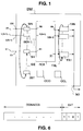
- the diagram in FIG. 2 represents a configuration of the multiplexer of the invention at a time interval it , the token JT1 being in the physical queue FA1.
- the token JT1 being in the physical queue FA1.
- the token JT1 being in the physical queue FA1.
- the token JT2 receives an occupied cell.
- These cells are routed successively in the upward circular direction of the network outputs.
- the occupied cell presented at entry R2 is routed to the physical queue FA2, that presented at entry R5 towards the queue FA3 and the one appearing at entry R6 to the physical queue FA4.
- the token JT2 passes into the queue FA2.
- the inputs R2, R3, R5 and R7 of the RCX network receive an occupied cell.
- this mesh achieves a perfect mixture between the columns, in the sense that the upper half and the lower half of the outputs are mixed regularly with the inputs.
- the reverse Omega network is obtained by symmetry of the Omega network with respect to a vertical line. It can also be easily defined independently by taking inspiration from the mesh law of the Omega network mentioned above, and by substituting for example RotD for RotG and by reversing the order of the columns which then becomes 0, 1, ..., K-1 according to the direction of transmission.
- the reverse Omega network being the mirror image of an Omega network
- the reverse order Omega network of order K can be constructed from two disjoint reverse reverse Omega networks of order K-1 and an additional column of binary switches of base located before the exit of the new network.
- the Omega network is a self-routing network where the routing binary elements are the binary elements indicating the destination address, the basic binary switches of the order n column testing the binary order n element of this address. It is the same for the reverse Omega network in which, according to the direction of transmission, the first column is numbered 0 while for the Omega network it is the last column which is thus numbered.
- This routing mode clearly separates the two types of cells, the occupied cells being allocated successively in the upward direction of the outputs and the free cells in the downward direction.
- the order K network consists of two orders of K - 1 network followed by a final patching stage.
- the index i varies from zero to N / 2 - 1
- the referral mode of order K-1 does a good separation outputs of this sub-network without internal blocking.
- the CCO counters of the addresses of the occupied cells of the first subnetwork reach a value U i .
- This value U i is taken as the initial position for the separation of the outputs of the second sub-network, that is to say when the global index i varies from N / 2 to N - 1.
- the order switching mode K-1 now performs separation without blocking inside this second sub-network.
- the routing mode of order K described does not present any blocking for the first K-1 columns. It remains to demonstrate that the last column does not present any blockage either. However, a block in this last column would simply mean that an address would have been assigned twice. This is impossible since the addresses of the outputs are all assigned each time once by the allocation mechanism to two counters described above.
- the network used is a simplified reverse Omega network which assumes that all the inputs are significant at all times, that the network does not broadcast and that the binary routing elements are calculated from so that for each crossing, there is no internal blockage inside the matrix.
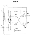
- the basic binary switch of the multiplexer of the present invention therefore essentially comprises four logic gates PT1 to PT4 of the AND type, two logic gates PT5 and PT6 of the OR type and a bistable BS.
- An input of the doors PT1 and PT2 is connected to an input lN1 of the switch, an input of the doors PT3 and PT4 being connected to another input lN2 of this switch.
- Another input of the doors PT1 and PT4 is connected to an output B1 of the bistable BS, another input of the doors PT2 and PT3 being connected to another output B0 of this bistable.
- a signal input of the bistable BS is connected to the input lN1 of the switch and the control input of this bistable is connected to a source of validation clock pulses Hg.
- Two inputs of the door PT5 are respectively connected to an output of the door PT1 and to an output of the door PT3, two inputs of the door PT6 being respectively connected to an output of the door PT2 and to an output of the door PT4.
- the output of the gate PT5 is connected to an output SS1 of the switch and the output of the gate PT6 is connected to an output SS2 of this switch, the operation of which is as follows: the clock pulse Hg validates the binary element d switch located in a fixed position in each cell. This binary element is memorized in the BS bistable during the time allocated to a cell.
- the bistable BS commands the switching of the basic binary switch so that the signal present at the input lN1 is retransmitted either on the output SS1 the signal present at the input lN2 then being retransmitted on the output SS2, or on the output SS2 the signal present at the input lN2 then being retransmitted on the output SS1.
- These two referral cases are the only ones authorized. It should be noted that it suffices to test the binary control element on a single input because the two inputs are significant and the routing is such that there is no conflict or duplication in the basic binary switch.
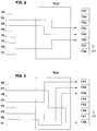
- FIG. 5 illustrates an exemplary embodiment of a reverse Omega network constituted using basic binary switches identical to that of FIG. 4. It should be noted that all the binary switches are exactly similar and extremely simple, which gives rise both to a regular implantation of high density in the integrated circuits, and to an extremely fast crossing time.
- timing circuits TT1, TT2 and TT3 arranged between each stage of the RCX switching network, the clock which supplies the Hg validation pulses is simply delayed by a delay equal to the time of crossing of a binary switch. base increased by the transmission time of a binary element. Originally, this clock is synchronized with the transmission of the first bit of each cell.
- the operation of the synchronization and header insertion loop SlE (FIG. 1) is as follows: the transmission time of this mouth is exactly equal to that of a cell at the rate entry. At each cell time, the mouth head BST knows the length of the logical queue, the identity of the first physical queue FAi to be used for the transmission of a cell and that of the first physical queue FAj to which must be sent a free cell and which is, as we saw previously, FA (i-1).
- the mouth head BST sends these three parameters by mouth to the first synchronization and insertion block Sl1, waits for the same parameters coming from the preceding synchronization block, SlN, delays to finish the cell time and starts these same operations again.
- the BST muzzle head knowing the output rhythm of the multiplexer, decrements the counter indicating the length of the queue according to this rhythm.
- the function of the synchronization and insertion blocks Sli is to transmit in synchronism each a cell after having assigned to it an internal switch header. This task is executed in sequence in the order of the mouth, because each synchronization block can only work after having received the parameters coming from the previous block.
- the synchronization block concerned In the case where there is no cell to send, the synchronization block concerned must send a free cell with the header equal to the free cell position it has received, and decrements (modulo N) the free cell position counter. Otherwise, the synchronization block checks the overflow of the logical queue FAL: if there is an overflow the cell is destroyed and the synchronization block behaves as in the previous case. In the absence of an overflow, the synchronization block increments the length of the logical queue FAL and sends the cell with the header equal to the position of the physical queue FAi which it has received and increments (modulo N) this position.
- the Sli synchronization and insertion block then returns the three parameters in the mouth, either for the next block, or for the BST mouth head.
- the loop head block BST can be entrusted with a central function for calculating all the headers before sending them successively to all the synchronization and insertion blocks via the loop described above; the synchronization blocks will then simply have to receive the header sent by the loop head BST instead of having to calculate it.
- the data to be transmitted occurring at input 0 of the basic binary switch of the first stage of the switching network is preceded by a header EnT identifying the output 13 , that is to say the binary word 1101.
- the least significant binary element of this word is read: "1".
- the data presented on the input 0 of the switch of the first stage are routed on the upper output of this switch. This data is therefore presented at the lower input of the base switch of the second stage of the switching network.
- the second least significant binary element of the header EnT is then read: "0".
- the data are therefore, in accordance with the invention, transmitted to the lower output of the binary switch of the second stage of the network to be supplied, following the mesh of the reverse Omega network of the invention, to the lower input of the binary switch of the third network floor.
- the third least significant binary element of the header EnT being a "1" the data is supplied to the upper output of the binary switch of this third stage to be forwarded to an input (the lower input) of a switch basic binary of the fourth and last stage of the switching network.
- the fourth least significant binary element of the header EnT i.e. the most significant binary element of this header, being a "1" the data is retransmitted on the upper output of the basic binary switch, that is to say on the output 13 of the network.
- the routing of the data supplied to inputs 2, 3, 6 and 7 through the switching network is carried out in a similar way: a header identifying the outputs 14, 15, 16 and 17 respectively is written in each occupied cell which is then routed through the reverse Omega switching network by successively reading the binary elements of these headers, starting with the least significant elements.
- a "1" controls the switch on the upper output and a "0" controls the switch on the lower output.
- the network only has 16 inputs and 16 outputs numbered from 0 to 15 and outputs 16 and 17 identified by the header of the cells supplied at inputs 6 and 7 are the two outputs respectively after the output. 15 by turning in the increasing direction, therefore the outputs 0 and 1.
Landscapes
- Engineering & Computer Science (AREA)
- Computer Hardware Design (AREA)
- Computer Networks & Wireless Communication (AREA)
- Signal Processing (AREA)
- Multimedia (AREA)
- Data Exchanges In Wide-Area Networks (AREA)
Abstract
Description
La présente invention a pour objet un multiplexeur asynchrone c'est-à-dire un dispositif comprenant une pluralité d'entrées et une seule sortie vers laquelle sont transmis les signaux d'entrée après multiplexage.The present invention relates to an asynchronous multiplexer, that is to say a device comprising a plurality of inputs and a single output to which the input signals are transmitted after multiplexing.
Elle est applicable dans les systèmes de transmission de données en mode asynchrone.It is applicable in data transmission systems in asynchronous mode.
Dans les systèmes de transmission du type synchrone la somme des débits des affluents à l'entrée d'un multiplexeur est égale au débit de sortie. Dans les systèmes asynchrones, il y a lieu de séparer le débit brut d'un affluent et le flot des cellules utiles qu'il transporte. Seule importe la comparaison de la sommes des débits utiles des différents affluents avec le débit brut de sortie. Cette somme varie avec le temps. En moyenne elle ne peut être égale au débit brut de sortie, mais, momentanément, elle peut le dépasser, et les cellules qui ne peuvent être émises à temps doivent être stockées dans une ou plusieurs files d'attente. Cette caractéristique, due à l'asynchronisme du mode de transfert, est à la fois source de souplesse en ce qui concerne le nombre et la vitesse brute des affluents, et complexité engendrée par la gestion des files d'attente et la régulation des flux entrants.In synchronous type transmission systems, the sum of the flows of the tributaries at the input of a multiplexer is equal to the output flow. In asynchronous systems, it is necessary to separate the gross flow of a tributary and the flow of useful cells that it transports. Only the comparison of the sum of the useful flows of the different tributaries with the gross output flow matters. This amount varies over time. On average, it cannot be equal to the gross output rate, but, momentarily, it can exceed it, and cells which cannot be sent in time must be stored in one or more queues. This characteristic, due to the asynchronism of the transfer mode, is both a source of flexibility with regard to the number and raw speed of the tributaries, and complexity generated by the management of queues and the regulation of incoming flows. .
La conception d'un multiplexeur asynchrone est donc un compromis entre ces deux facteurs.The design of an asynchronous multiplexer is therefore a compromise between these two factors.
Une des caractéristiques du multiplexeur asynchrone à N entrées et une sortie de l'invention réside dans le fait qu'il comprend une boucle de synchronisation et d'insertion d'en-tête composée de N blocs de synchronisation et d'insertion sur les entrées desquels sont respectivement connectées N lignes entrantes, un réseau de commutation à N entrées et N sorties, dont les entrées sont respectivement connectées aux sorties des blocs de synchronisation et d'insertion, et une file d'attente logique constituée de N files physiques connectées en boucle, lues successivement en ordre séquentiel circulaire, dont les entrées sont respectivement connectées aux sorties du réseau de commutation et dont les sorties sont connectées à la sortie du multiplexeur.One of the characteristics of the asynchronous multiplexer with N inputs and one output of the invention resides in the fact that it comprises a synchronization and header insertion loop composed of N synchronization and insertion blocks on the inputs of which N incoming lines are respectively connected, a switching network with N inputs and N outputs, the inputs of which are respectively connected to the outputs of synchronization and insertion blocks, and a logical queue made up of N physical queues connected in a loop, successively read in circular sequential order, the inputs of which are respectively connected to the outputs of the switching network and the outputs of which are connected to the output of the multiplexer.
Une autre caractéristique du multiplexeur de l'invention réside dans le fait que ledit réseau de commutation est un réseau équivalent du point de vue logique à un réseau du type Oméga inverse.Another characteristic of the multiplexer of the invention lies in the fact that said switching network is a network which is logically equivalent to a network of the reverse Omega type.
Une autre caractéristique du multiplexeur de l'invention réside dans le fait qu'il comprend également, dans la boucle de synchronisation et d'insertion, un bloc supplémentaire de tête de boucle.Another characteristic of the multiplexer of the invention lies in the fact that it also comprises, in the synchronization and insertion loop, an additional block of the loop head.
Une autre caractéristique du multiplexeur de l'invention réside dans le fait qu'il comprend en outre un premier compteur décrémenté d'une unité à l'arrivée de chaque cellule libre lors de l'exploration des entrées du multiplexeur pour donner l'adresse d'aiguillage des cellules libres entrantes successives dans les files d'attente de sortie.Another characteristic of the multiplexer of the invention lies in the fact that it further comprises a first counter decremented by one unit at the arrival of each free cell during the exploration of the inputs of the multiplexer to give the address d referral of successive incoming free cells in the exit queues.
Une autre caractéristique du multiplexeur de l'invention réside dans le fait qu'il comprend également un second compteur incrémenté d'une unité à l'arrivée de chaque cellule occupée lors de l'exploration des entrées du multiplexeur pour donner l'adresse d'aiguillage des cellules occupées entrantes successives dans les files d'attente de sortie.Another characteristic of the multiplexer of the invention resides in the fact that it also includes a second counter incremented by one unit at the arrival of each occupied cell when exploring the inputs of the multiplexer to give the address of referral of successive incoming occupied cells to exit queues.
Les différents objets et caractéristiques de l'invention seront maintenant détaillés dans la description qui va suivre, faite à titre d'exemple non limitatif, en se reportant aux figures annexées qui représentent :
- la figure 1, la structure d'un multiplexeur conçu conformément à la présente invention ;
- les figures 2, le schéma simplifié du multiplexeur de la figure 1 à un instant it ;
- la figure 3, le schéma simplifié du multiplexeur de la figure 2 à un instant it+1 ;
- la figure 4, un exemple de réalisation d'un commutateur binaire de base du réseau de commutation RCX des figures précédentes conçu conformément à l'invention ;
- la figure 5, un exemple de réalisation d'un réseau de commutation du type Oméga inverse à huit entrées et huit sorties conçu conformément à la présente invention ;
- la figure 6, un exemple d'en-tête d'aiguillage associé à une cellule occupée.
- Figure 1, the structure of a multiplexer designed in accordance with the present invention;
- Figures 2, the simplified diagram of the multiplexer of Figure 1 at a time it;
- FIG. 3, the simplified diagram of the multiplexer of FIG. 2 at an instant it + 1;
- FIG. 4, an exemplary embodiment of a basic binary switch of the RCX switching network of the preceding figures designed in accordance with the invention;
- FIG. 5, an exemplary embodiment of a switching network of the reverse Omega type with eight inputs and eight outputs designed in accordance with the present invention;
- FIG. 6, an example of a referral header associated with an occupied cell.
On décrira maintenant, en se reportant au schéma de la figure 1, un exemple de réalisation d'un multiplexeur asynchrone conçu conformément à la présente invention.A description will now be given, with reference to the diagram of FIG. 1, of an embodiment of an asynchronous multiplexer designed in accordance with the present invention.
Le multiplexeur de la figure 1 se présente sous la forme d'un bloc BM comprenant N entrées référencées E1 à EN, N étant une puissance de 2, et une sortie S0. Sur les entrées E1 à EN, connectées chacune à une ligne entrante L1 à LN, sont fournis des affluents de même débit brut, le débit brut de sortie pouvant être quelconque.The multiplexer of FIG. 1 is in the form of a block BM comprising N inputs referenced E1 to EN, N being a power of 2, and an output S0. On the inputs E1 to EN, each connected to an incoming line L1 to LN, tributaries of the same gross flow rate are supplied, the gross output flow rate being arbitrary.
Le multiplexeur de la figure 1 comprend également une boucle de synchronisation et d'insertion d'en-tête SlE composée de N blocs de synchronisation et d'insertion Sl1 à SlN et d'un bloc supplémentaire de tête de boucle BST.The multiplexer of FIG. 1 also includes a synchronization and header insertion loop SlE composed of N synchronization and insertion blocks Sl1 to SlN and an additional block of the loop head BST.
Chaque ligne entrante est respectivement connectée à une entrée d'un bloc de synchronisation et d'insertion Sl1 à SlN.Each incoming line is respectively connected to an input of a synchronization and insertion block Sl1 to SlN.
Le multiplexeur de la figure 1 comprend également un réseau de commutation RCX à N entrées R1 à RN et N sorties X1 à XN. Les entrées R1 à RN de ce réseau sont respectivement connectées à des sorties non référencées des blocs de synchronisation Sl1 à SlN. Ces blocs émettent en synchronisme sur ces entrées.The multiplexer of FIG. 1 also includes a switching network RCX with N inputs R1 to RN and N outputs X1 to XN. The inputs R1 to RN of this network are respectively connected to non-referenced outputs of the synchronization blocks Sl1 to SlN. These blocks transmit synchronously to these inputs.
Le multiplexeur de la figure 1 comprend en outre une file d'attente logique FAL constituée de N files physiques FA1 à FAN connectées en boucle, lues successivement en ordre séquentiel circulaire, dont les sorties sont connectées à la sortie S0. Des entrées non référencées de ces files sont respectivement connectées aux sorties X1 à XN du réseau RCX qui retransmet, en parallèle, les cellules occupées issues des lignes entrantes L1 à LN sur ces entrées.The multiplexer of FIG. 1 further comprises a logical queue FAL made up of N physical queues FA1 to FAN connected in a loop, successively read in circular sequential order, the outputs of which are connected to the output S0. Unreferenced inputs of these queues are respectively connected to the outputs X1 to XN of the RCX network which retransmits, in parallel, the occupied cells originating from the incoming lines L1 to LN on these inputs.
Selon un mode de réalisation préféré le réseau de commutation RCX est un réseau logiquement équivalent à un réseau de type Oméga inversé. C'est ce type de réseau qui, pour faciliter la description et la compréhension, sera considéré dans ce qui va suivre.According to a preferred embodiment, the RCX switching network is a network logically equivalent to a network of the reverse Omega type. It is this type of network which, to facilitate description and understanding, will be considered in what follows.
Un réseau Oméga est un réseau de type connu appartenant à la classe des réseaux "delta", eux-mêmes dérivés des réseaux dits "banyan", réseaux multi-étages dont une des caractéristiques réside dans le fait qu'ils comprennent un trajet bien défini entre une entrée quelconque et une sortie quelconque. Comme les réseaux delta, les réseaux Oméga sont également caractérisés par le fait que le routage à travers ces réseaux est commandé à l'aide d'éléments binaires internes.An Omega network is a known type network belonging to the class of "delta" networks, themselves derived from so-called "banyan" networks, multi-stage networks one of the characteristics of which is that they include a well-defined path. between any input and any output. Like delta networks, Omega networks are also characterized by the fact that routing through these networks is controlled using internal binary elements.
Un réseau Oméga à N entrées et N sorties, constitué d'éléments de commutation élémentaires ou commutateurs binaires de base à 2 entrées et 2 sorties comprend K = Log₂ N étages, chaque étage comprenant N/2 éléments de commutation. Il est auto-acheminant, et utilise une adresse de destination à K éléments binaires.An Omega network with N inputs and N outputs, consisting of elementary switching elements or basic binary switches with 2 inputs and 2 outputs comprises K = Log₂ N stages, each stage comprising N / 2 switching elements. It is self-routing, and uses a destination address with K bits.
D'une façon générale, le réseau Oméga peut fonctionner aussi bien en mode synchrone qu'en mode asynchrone. Mais, alors qu'il peut commuter des paquets simultanés et en parallèle, c'est un réseau bloquant, c'est-à-dire qu'il peut y avoir collision entre des paquets qui sont alors soit perdus soit retardé l'un derrière l'autre. Pour pallier ces inconvénients une solution consiste à augmenter la vitesse de fonctionnement du réseau.In general, the Omega network can operate in both synchronous and asynchronous modes. But, while it can switch simultaneous and parallel packets, it is a blocking network, i.e. there can be a collision between packets which are then either lost or delayed one behind the other. To overcome these drawbacks, one solution consists in increasing the operating speed of the network.
Une autre solution consiste à placer des mémoires tampons dans chaque étage du réseau de commutation.Another solution is to place buffer memories in each stage of the switching network.
Le multiplexeur proposé évite ces deux contraintes. Il est basé, notamment, sur un nouveau calcul du routage des cellules à l'intérieur du réseau.The proposed multiplexer avoids these two constraints. It is based, in particular, on a new calculation of the routing of cells inside the network.
Le multiplexeur de la figure 1 comprend donc à cet effet un premier compteur CCL utilisé pour gérer le routage des cellules libres et un compteur CCO utilisé pour gérer le routage des cellules occupées.The multiplexer of FIG. 1 therefore comprises for this purpose a first CCL counter used to manage the routing of free cells and a CCO counter used to manage the routing of occupied cells.
Le compteur CCL est décrémenté d'une unité à l'arrivée de chaque cellule libre lors de l'exploration des entrées du multiplexeur alors que le compteur CCO est incrémenté d'une unité à l'apparition de chaque cellule occupée lors de l'exploration de ces entrées.The CCL counter is decremented by one unit at the arrival of each free cell when exploring the inputs of the multiplexer while the CCO counter is incremented by one unit at the appearance of each occupied cell during exploration of these entries.
Les cellules libres sont ainsi routées successivement dans le sens circulaire descendant des sorties du réseau Oméga inversé, ces cellules n'étant pas prises en compte par les files d'attente, et les cellules occupées sont routées successivement dans le sens circulaire montant des sorties de ce réseau.The free cells are thus routed successively in the circular direction descending from the outputs of the reverse Omega network, these cells not being taken into account by the queues, and the occupied cells are routed successively in the circular direction rising from the outputs of this network.
Ce nouveau mode de fonctionnement est illustré par les schémas des figures 2 et 3 où, par simplification, on a supposé que le rythme d'entrée et le rythme de sortie étaient égaux.This new mode of operation is illustrated by the diagrams of FIGS. 2 and 3 where, for simplicity, it has been assumed that the rate of entry and the rate of exit are equal.
Le schéma de la figure 2 représente une configuration du multiplexeur de l'invention à un intervalle de temps it, le jeton JT1 étant dans la file d'attente physique FA1. A cet instant, seules les entrées R2, R5, et R6 du réseau RCX reçoivent une cellule occupée. Ces cellules sont routées successivement dans le sens circulaire montant des sorties du réseau. Ainsi, la cellule occupée présentée à l'entrée R2 est aiguillée vers la file d'attente physique FA2, celle présentée à l'entrée R5 vers la file d'attente FA3 et celle se présentant à l'entrée R6 vers la file d'attente physique FA4. A l'intervalle de temps suivant it+1, comme le montre le schéma de la figure 3, le jeton JT2 passe dans la file d'attente FA2. Selon l'exemple choisi, seules les entrées R2, R3, R5 et R7 du réseau RCX reçoivent une cellule occupée. Ces cellules sont aiguillées respectivement vers les files d'attente FA5, FA6, FA7, et FA8, la prochaine cellule occupée qui se présentera étant aiguillée vers la file d'attente suivante, la file FA1 selon l'exemple choisi, le réseau RCX n'ayant, pour simplifier, que 8 entrées et 8 sorties, la file d'attente FAL ne comprenant alors que 8 files d'attente physiques.The diagram in FIG. 2 represents a configuration of the multiplexer of the invention at a time interval it , the token JT1 being in the physical queue FA1. At this time, only the inputs R2, R5, and R6 of the RCX network receive an occupied cell. These cells are routed successively in the upward circular direction of the network outputs. Thus, the occupied cell presented at entry R2 is routed to the physical queue FA2, that presented at entry R5 towards the queue FA3 and the one appearing at entry R6 to the physical queue FA4. At the time interval following it + 1, as shown in the diagram in FIG. 3, the token JT2 passes into the queue FA2. According to the example chosen, only the inputs R2, R3, R5 and R7 of the RCX network receive an occupied cell. These cells are routed respectively to the queues FA5, FA6, FA7, and FA8, the next occupied cell which will appear being routed to the next queue, the queue FA1 according to the example chosen, the network RCX n 'having, for simplicity, only 8 inputs and 8 outputs, the FAL queue then comprising only 8 physical queues.
On va montrer maintenant que ce nouveau mode ou algorithme d'aiguillage entraîne un routage sans blocage dans le réseau Oméga inversé.We will now show that this new mode or referral algorithm involves routing without blocking in the reverse Omega network.
Un réseau Oméga à N entrées et N sorties, N étant comme on l'a vu précédemment une puissance de deux, est une matrice d'interconnexion de Log₂ N colonnes et de N/2 lignes de commutateurs binaires de base, dont la loi de maillage est la suivante :
- pour toute colonne de commutateurs binaires de base, la sortie i est connectée à l'entrée i = RotG(i) de la colonne suivante dans le sens de la transmission, i étant un nombre binaire de Log₂ N éléments binaires et RotG(i) étant le nombre binaire obtenu à partir de i par une rotation à gauche de i d'une position et RotD(i) correspondant à une rotation à droite.
- les colonnes de commutateurs binaires de base sont numérotées dans l'ordre décroissant K-1, K-2, ..., 0 dans le sens de transmission.
- les fils d'interconnexion sont numérotés de bas en haut, un fil ayant deux numéros différents selon qu'il est considéré comme la sortie d'un commutateur binaire de base ou comme l'entrée du commutateur binaire suivant. Il en est de même pour les fils d'entrée de la matrice, car le même maillage s'applique entre les entrées de la matrice et les entrées de la première colonne de commutateurs. La numérotation des fils de sortie est la même, que ce soit comme sorties de la matrice ou comme sorties de la dernière colonne de commutateurs binaires de base.
- for any column of basic binary switches, the output i is connected to the input i = RotG (i) of the next column in the direction of transmission, i being a binary number of Log₂ N binary elements and RotG (i) being the binary number obtained from i by a left rotation of i of a position and RotD (i) corresponding to a right rotation.
- the basic binary switch columns are numbered in descending order K-1, K-2, ..., 0 in the direction of transmission.
- the interconnection wires are numbered from bottom to top, a wire having two different numbers depending on whether it is considered as the output of a basic binary switch or as the input of the next binary switch. The same is true for the input wires of the matrix, since the same mesh applies between the inputs of the matrix and the inputs of the first column of switches. The numbering of the output wires is the same, whether as outputs from the matrix or as outputs from the last column of basic binary switches.
On dit que ce maillage réalise un mélange parfait entre les colonnes, dans le sens que la moitié haute et la moitié basse des sorties sont mélangées régulièrement aux entrées.We say that this mesh achieves a perfect mixture between the columns, in the sense that the upper half and the lower half of the outputs are mixed regularly with the inputs.
Le réseau Oméga inverse s'obtient par symétrie du réseau Oméga par rapport à une droite verticale. Il peut aussi se définir aisément de façon autonome en s'inspirant de la loi de maillage du réseau Oméga précédemment citée, et en substituant par exemple RotD à RotG et en inversant l'ordre des colonnes qui devient alors 0, 1, ..., K-1 selon le sens de transmission.The reverse Omega network is obtained by symmetry of the Omega network with respect to a vertical line. It can also be easily defined independently by taking inspiration from the mesh law of the Omega network mentioned above, and by substituting for example RotD for RotG and by reversing the order of the columns which then becomes 0, 1, ..., K-1 according to the direction of transmission.
On sait déjà qu'un réseau Oméga d'ordre K (avec K = Log₂ N) peut être construit à partir de deux réseaux Oméga disjoints d'ordre K-1 et d'une colonne supplémentaire de commutateurs binaires de base située après l'entrée du nouveau réseau. Le réseau Oméga inverse étant l'image miroir d'un réseau Oméga, le réseau Oméga inverse d'ordre K peut être construit à partir de deux réseaux Oméga inverses disjoints d'ordre K-1 et d'une colonne supplémentaire de commutateurs binaires de base située avant la sortie du nouveau réseau.We already know that an Omega network of order K (with K = Log₂ N) can be constructed from two disjoint Omega networks of order K-1 and an additional column of basic binary switches located after the entry of the new network. The reverse Omega network being the mirror image of an Omega network, the reverse order Omega network of order K can be constructed from two disjoint reverse reverse Omega networks of order K-1 and an additional column of binary switches of base located before the exit of the new network.
En outre, le réseau Oméga est un réseau auto-acheminant où les éléments binaires de routage sont les éléments binaires indiquant l'adresse de destination, les commutateurs binaires de base de la colonne d'ordre n testant l'élément binaire d'ordre n de cette adresse. Il en est de même pour le réseau Oméga inverse dans lequel, selon le sens de transmission, la première colonne est numérotée 0 alors que pour le réseau Oméga c'est la dernière colonne qui est ainsi numérotée.In addition, the Omega network is a self-routing network where the routing binary elements are the binary elements indicating the destination address, the basic binary switches of the order n column testing the binary order n element of this address. It is the same for the reverse Omega network in which, according to the direction of transmission, the first column is numbered 0 while for the Omega network it is the last column which is thus numbered.
On rappelle que, à un instant quelconque, l'adresse de destination de la prochaine cellule occupée se présentant à l'entrée du réseau Oméga inversé est donnée par le compteur CCO. Soit Ji cette adresse. L'adresse de destination de la prochaine cellule libre, donnée par le contenu du compteur CCL est alors, comme on l'a vu précédemment, Ji -1, en arithmétique modulo N.It will be recalled that, at any time, the destination address of the next occupied cell appearing at the input of the reverse Omega network is given by the CCO counter. Let J i be this address. The destination address of the next free cell, given by the content of the CCL counter is then, as we saw previously, J i -1, in modulo N arithmetic.
Ce mode de routage sépare bien les deux types de cellules, les cellules occupées étant attribuées successivement dans le sens montant des sorties et les cellules libres dans le sens descendant.This routing mode clearly separates the two types of cells, the occupied cells being allocated successively in the upward direction of the outputs and the free cells in the downward direction.
Il est bien évident que cet aiguillage est sans blocage pour un commutateur binaire de base puisque dans tous les cas possibles les adresses de destination sont différentes. On suppose qu'il en est de même pour les réseaux Oméga inverses d'ordre inférieur à K.It is obvious that this routing is without blocking for a basic binary switch since in all possible cases the destination addresses are different. We assume that the same is true for reverse Omega networks of order lower than K.
On a vu précédemment que le réseau d'ordre K est constitué de deux réseaux d'ordre K - 1 suivi d'un dernier étage de brassage. Quand l'indice i varie de zéro à N/2 - 1, si on considère le sous réseau bas, avec la position initiale Rotg(Ji)/2, le mode d'aiguillage d'ordre K-1 réalise bien une séparation des sorties de ce sous réseau sans blocage interne. Après que l'entrée d'indice N/2 - 1 ait été considérée, le compteurs CCO des adresses des cellules occupées du premier sous réseau atteint une valeur Ui.We have previously seen that the order K network consists of two orders of K - 1 network followed by a final patching stage. When the index i varies from zero to N / 2 - 1, if we consider the low sub-network, with the initial position Rotg (J i ) / 2, the referral mode of order K-1 does a good separation outputs of this sub-network without internal blocking. After the entry of index N / 2 - 1 has been considered, the CCO counters of the addresses of the occupied cells of the first subnetwork reach a value U i .
Cette valeur Ui est reprise comme position initiale pour la séparation des sorties du deuxième sous réseau, c'est-à-dire quand l'indice global i varie de N/2 à N - 1. Le mode d'aiguillage d'ordre K-1 réalise maintenant une séparation sans blocage à l'intérieur de ce deuxième sous réseau.This value U i is taken as the initial position for the separation of the outputs of the second sub-network, that is to say when the global index i varies from N / 2 to N - 1. The order switching mode K-1 now performs separation without blocking inside this second sub-network.
On peut remarquer qu'en appliquant ce mode d'aiguillage de façon globale au réseau d'ordre K, l'attribution des chemins induit les mêmes sous chemins que ceux obtenus séparément comme on vient de le voir. En effet, par la loi de brassage partait, la succession des sorties de la matrice d'ordre K correspond à la succession des commutateurs binaires de base de la dernière colonne, qui correspond elle même à la succession des sorties d'une des deux sous matrices. De plus, cette correspondance est par définition obtenue par une rotation à gauche, puisque le maillage dans le sens de transmission est défini par une rotation à droite.One can notice that by applying this mode of referral in a global way to the network of order K, the allocation of the paths induces the same under paths as those obtained separately as we have just seen. Indeed, by the mixing law started, the succession of the outputs of the matrix of order K corresponds to the succession of the basic binary switches of the last column, which itself corresponds to the succession of the outputs of one of the two sub matrices. In addition, this correspondence is by definition obtained by a rotation to the left, since the mesh in the direction of transmission is defined by a rotation to the right.
En conclusion, le mode de routage d'ordre K décrit ne présente pas de blocage pour les K-1 premières colonnes. Il reste à démontrer que la dernière colonne ne présente pas non plus de blocage. Or un blocage dans cette dernière colonne signifierait tout simplement qu'une adresse aurait été attribuée deux fois. Ceci est impossible puisque les adresses des sorties sont toutes attribuées chacune une fois par le mécanisme d'attribution à deux compteurs décrit précédemment.In conclusion, the routing mode of order K described does not present any blocking for the first K-1 columns. It remains to demonstrate that the last column does not present any blockage either. However, a block in this last column would simply mean that an address would have been assigned twice. This is impossible since the addresses of the outputs are all assigned each time once by the allocation mechanism to two counters described above.
Compte tenu de ce qui vient d'être décrit le réseau utilisé est un réseau Oméga inversé simplifié qui suppose que toutes les entrées sont significatives à chaque instant, que le réseau ne fait pas de diffusion et que les éléments binaires d'aiguillage sont calculés de telle façon que pour chaque traversée, il n'y a aucun blocage interne à l'intérieur de la matrice. Ces hypothèses simplificatrices permettent de concevoir un commutateur binaire de base très simplifié dont un exemple de réalisation est illustré par le schéma de la figure 4. En effet, dans sa forme générale, la logique d'un tel commutateur est relativement complexe car il faut tenir compte des contentions possibles quand deux entrées sont destinées à la même sortie, et éventuellement plus complexe si l'on désire faire de la diffusion d'une entrée sur les deux sorties.In view of what has just been described, the network used is a simplified reverse Omega network which assumes that all the inputs are significant at all times, that the network does not broadcast and that the binary routing elements are calculated from so that for each crossing, there is no internal blockage inside the matrix. These simplifying hypotheses make it possible to design a very simplified basic binary switch, an exemplary embodiment of which is illustrated by the diagram in FIG. 4. In fact, in its general form, the logic of such a switch is relatively complex because it is necessary to take account of possible contention when two entries are intended for the same exit, and possibly more complex if one wishes to make the diffusion of an entry on the two exits.
Le commutateur binaire de base du multiplexeur de la présente invention comprend donc essentiellement quatre portes logiques PT1 à PT4 du type ET, deux portes logiques PT5 et PT6 du type OU et un bistable BS.The basic binary switch of the multiplexer of the present invention therefore essentially comprises four logic gates PT1 to PT4 of the AND type, two logic gates PT5 and PT6 of the OR type and a bistable BS.
Une entrée des portes PT1 et PT2 est connectée à une entrée lN1 du commutateur, une entrée des portes PT3 et PT4 étant connectée à une autre entrée lN2 de ce commutateur. Une autre entrée des portes PT1 et PT4 est connectée à une sortie B1 du bistable BS, une autre entrée des portes PT2 et PT3 étant connectée à une autre sortie B0 de ce bistable. Une entrée de signal du bistable BS est connectée à l'entrée lN1 du commutateur et l'entrée de commande de ce bistable est connectée à une source d'impulsions d'horloge Hg de validation. Deux entrées de la porte PT5 sont respectivement connectées à une sortie de la porte PT1 et à une sortie de la porte PT3, deux entrées de la porte PT6 étant respectivement connectées à une sortie de la porte PT2 et à une sortie de la porte PT4. La sortie de la porte PT5 est connectée à une sortie SS1 du commutateur et la sortie de la porte PT6 est connectée à une sortie SS2 de ce commutateur dont le fonctionnement est le suivant : l'impulsion d'horloge Hg valide l'élément binaire d'aiguillage qui se trouve à une position fixe dans chaque cellule. Cet élément binaire est mémorisé dans le bistable BS durant le temps alloué à une cellule. Le bistable BS commande la commutation du commutateur binaire de base de telle sorte que le signal présent à l'entrée lN1 est retransmis soit sur la sortie SS1 le signal présent à l'entrée lN2 étant alors retransmis sur la sortie SS2, soit sur la sortie SS2 le signal présent à l'entrée lN2 étant alors retransmis sur la sortie SS1. Ces deux cas d'aiguillage sont les seuls autorisés. Il est à noter qu'il suffit de tester l'élément binaire de commande sur une seule entrée car les deux entrées sont significatives et l'aiguillage est tel qu'il y ait ni conflit ni duplication dans le commutateur binaire de base.An input of the doors PT1 and PT2 is connected to an input lN1 of the switch, an input of the doors PT3 and PT4 being connected to another input lN2 of this switch. Another input of the doors PT1 and PT4 is connected to an output B1 of the bistable BS, another input of the doors PT2 and PT3 being connected to another output B0 of this bistable. A signal input of the bistable BS is connected to the input lN1 of the switch and the control input of this bistable is connected to a source of validation clock pulses Hg. Two inputs of the door PT5 are respectively connected to an output of the door PT1 and to an output of the door PT3, two inputs of the door PT6 being respectively connected to an output of the door PT2 and to an output of the door PT4. The output of the gate PT5 is connected to an output SS1 of the switch and the output of the gate PT6 is connected to an output SS2 of this switch, the operation of which is as follows: the clock pulse Hg validates the binary element d switch located in a fixed position in each cell. This binary element is memorized in the BS bistable during the time allocated to a cell. The bistable BS commands the switching of the basic binary switch so that the signal present at the input lN1 is retransmitted either on the output SS1 the signal present at the input lN2 then being retransmitted on the output SS2, or on the output SS2 the signal present at the input lN2 then being retransmitted on the output SS1. These two referral cases are the only ones authorized. It should be noted that it suffices to test the binary control element on a single input because the two inputs are significant and the routing is such that there is no conflict or duplication in the basic binary switch.
La figure 5 illustre un exemple de réalisation d'un réseau Oméga inverse constitué à l'aide de commutateurs binaires de base identiques à celui de la figure 4. Il est à noter que tous les commutateurs binaires sont exactement semblables et extrêmement simples, ce qui donne lieu à la fois à une implantation régulière de densité élevée dans les circuits intégrés, et à un temps de traversée extrêmement rapide. Par l'intermédiaire de circuits de temporisation TT1, TT2 et TT3 disposés entre chaque étage du réseau de commutation RCX, l'horloge qui fournit les impulsions Hg de validation est simplement retardée d'un délai égal au temps de traversée d'un commutateur binaire de base augmenté du temps de transmission d'un élément binaire. A l'origine, cette horloge est synchronisée avec la transmission du premier élément binaire de chaque cellule.FIG. 5 illustrates an exemplary embodiment of a reverse Omega network constituted using basic binary switches identical to that of FIG. 4. It should be noted that all the binary switches are exactly similar and extremely simple, which gives rise both to a regular implantation of high density in the integrated circuits, and to an extremely fast crossing time. By means of timing circuits TT1, TT2 and TT3 arranged between each stage of the RCX switching network, the clock which supplies the Hg validation pulses is simply delayed by a delay equal to the time of crossing of a binary switch. base increased by the transmission time of a binary element. Originally, this clock is synchronized with the transmission of the first bit of each cell.
Compte tenu de ce qui précède, le fonctionnement de la boucle de synchronisation et d'insertion d'en-tête SlE (figure 1) est le suivant : le temps de transmission de cette bouche est exactement égal à celui d'une cellule au débit d'entrée. A chaque temps de cellule, la tête de bouche BST connaît la longueur de la file d'attente logique, l'identité de la première file physique FAi à être utilisée pour la transmission d'une cellule et celle de la première file physique FAj à laquelle doit être envoyée une cellule libre et qui est, comme on l'a vu précédemment, FA(i-1).In view of the above, the operation of the synchronization and header insertion loop SlE (FIG. 1) is as follows: the transmission time of this mouth is exactly equal to that of a cell at the rate entry. At each cell time, the mouth head BST knows the length of the logical queue, the identity of the first physical queue FAi to be used for the transmission of a cell and that of the first physical queue FAj to which must be sent a free cell and which is, as we saw previously, FA (i-1).
La tête de bouche BST envoie par la bouche ces trois paramètres au premier bloc de synchronisation et d'insertion Sl1, attend les mêmes paramètres venant du bloc de synchronisation précédent, SlN, temporise pour finir le temps de cellule et recommence ces mêmes opérations.The mouth head BST sends these three parameters by mouth to the first synchronization and insertion block Sl1, waits for the same parameters coming from the preceding synchronization block, SlN, delays to finish the cell time and starts these same operations again.
Parallèlement, la tête de bouche BST, connaissant le rythme de sortie du multiplexeur, décrémente le compteur indiquant la longueur de la file d'attente selon ce rythme.At the same time, the BST muzzle head, knowing the output rhythm of the multiplexer, decrements the counter indicating the length of the queue according to this rhythm.
Les blocs de synchronisation et d'insertion Sli ont pour fonction d'émettre en synchronisme chacun une cellule après avoir assigné à celle-ci un en-tête interne d'aiguillage. Cette tâche est exécutée en séquence dans l'ordre de la bouche, car chaque bloc de synchronisation ne peut travailler qu'après avoir reçu les paramètres venant du bloc précédent.The function of the synchronization and insertion blocks Sli is to transmit in synchronism each a cell after having assigned to it an internal switch header. This task is executed in sequence in the order of the mouth, because each synchronization block can only work after having received the parameters coming from the previous block.
Dans le cas où il n'y a pas de cellule à envoyer, le bloc de synchronisation concerné devra envoyer une cellule libre avec l'en-tête égal à la position de cellule libre qu'il a reçue, et décrémente (modulo N) le compteur de position des cellules libres. Dans le cas contraire, le bloc de synchronisation vérifie le débordement de la file d'attente logique FAL : si il y a débordement la cellule est détruite et le bloc de synchronisation se comporte comme dans le cas précédent. En l'absence de débordement, le bloc de synchronisation incrémente la longueur de la file d'attente logique FAL et envoie la cellule avec l'en-tête égal à la position de la file physique FAi qu'il a reçue et incrémente (modulo N) cette position.In the case where there is no cell to send, the synchronization block concerned must send a free cell with the header equal to the free cell position it has received, and decrements (modulo N) the free cell position counter. Otherwise, the synchronization block checks the overflow of the logical queue FAL: if there is an overflow the cell is destroyed and the synchronization block behaves as in the previous case. In the absence of an overflow, the synchronization block increments the length of the logical queue FAL and sends the cell with the header equal to the position of the physical queue FAi which it has received and increments (modulo N) this position.
Le bloc de synchronisation et d'insertion Sli renvoie alors les trois paramètres dans la bouche, soit pour le bloc suivant, soit pour la tête de bouche BST.The Sli synchronization and insertion block then returns the three parameters in the mouth, either for the next block, or for the BST mouth head.
Finalement, tous les blocs de synchronisation et d'insertion Sli envoient en synchronisme les cellules qu'ils ont à envoyer dans le réseau Oméga inverse.Finally, all the Sli synchronization and insertion blocks send the cells they have to send in the reverse Omega network in synchronism.
Dans une réalisation alternative, on peut confié au bloc de tête de boucle BST une fonction centrale de calcul de tous les en-têtes avant de les envoyer successivement à tous les blocs de synchronisation et d'insertion via la boucle décrite ci-dessus ; les blocs de synchronisation auront alors simplement à recevoir l'en-tête envoyé par la tête de boucle BST au lieu d'avoir à le calculer.In an alternative embodiment, the loop head block BST can be entrusted with a central function for calculating all the headers before sending them successively to all the synchronization and insertion blocks via the loop described above; the synchronization blocks will then simply have to receive the header sent by the loop head BST instead of having to calculate it.
On a représenté, sur le schéma de la figure 5 le trajet, conformément au mode d'aiguillage de l'invention, à travers un réseau Oméga simplifié conformément à l'invention de cinq cellules occupées se présentant respectivement et dans cet ordre sur les entrées 0, 2, 3, 6 et 7 de ce réseau pour être respectivement retransmises aux sorties 13, 14, 15, 0 et 1 de ce réseau à 16 entrées et 16 sorties, les cellules occupées étant retransmises successivement dans le sens circulaire montant des sorties du réseau à partir de la sortie 13 et les cellules libres étant retransmises successivement dans le sens circulaire descendant des sorties à partir de la sortie 13 - 1 = 12.The diagram in FIG. 5 shows the route, in accordance with the referral method of the invention, through a simplified Omega network in accordance with the invention of five occupied cells appearing respectively and in this order on the
Selon cet exemple, comme le montre le schéma de la figure 6, les données à transmettre se présentant à l'entrée 0 du commutateur binaire de base du premier étage du réseau de commutation sont précédées d'un en-tête EnT identifiant la sortie 13, c'est-à-dire le mot binaire 1101. Lors de la traversée du premier étage de rang 0 il est procédé à la lecture de l'élément binaire de poids le plus faible de ce mot : "1". Conformément au mode d'aiguillage de l'invention et de la constitution des commutateurs binaires de base qui en résulte, les données présentées sur l'entrée 0 du commutateur du premier étage sont aiguillées sur la sortie supérieure de ce commutateur. Ces données sont donc présentées à l'entrée inférieure du commutateur de base du second étage du réseau de commutation. Il est alors procédé à la lecture du second élément binaire de poids faible de l'en-tête EnT : "0". Les données sont donc, conformément à l'invention, transmises à la sortie inférieure du commutateur binaire du second étage du réseau pour être fournies, suite au maillage du réseau Oméga inverse de l'invention, à l'entrée inférieure du commutateur binaire du troisième étage du réseau. Le troisième élément binaire de poids faible de l'en-tête EnT étant un "1" les données sont fournies à la sortie supérieure du commutateur binaire de ce troisième étage pour être retransmis à une entrée (l'entrée inférieure) d'un commutateur binaire de base du quatrième et dernier étage du réseau de commutation. Le quatrième élément binaire de poids faible de l'en-tête EnT, c'est-à-dire l'élément binaire de poids le plus élevé de cet en-tête, étant un "1" les données sont retransmises sur la sortie supérieure du commutateur binaire de base, c'est-à-dire sur la sortie 13 du réseau. Le routage des données fournies aux entrées 2, 3, 6 et 7 à travers le réseau de commutation s'effectue de façon similaire : un en-tête identifiant respectivement les sorties 14, 15, 16 et 17 est inscrit dans chaque cellule occupée qui est alors aiguillée à travers le réseau de commutation Oméga inverse en lisant successivement les éléments binaires de ces en-têtes en commençant par les éléments de poids le plus faible. Un "1" commande l'aiguillage sur la sortie supérieure et un "0" commande l'aiguillage sur la sortie inférieure. Dans l'exemple choisi le réseau ne comporte que 16 entrées et 16 sorties numérotées de 0 à 15 et les sorties 16 et 17 identifiées par l'en-tête des cellules fournies aux entrées 6 et 7 sont respectivement les deux sorties venant après la sortie 15 en tournant dans le sens croissant, donc les sorties 0 et 1.According to this example, as shown in the diagram in FIG. 6, the data to be transmitted occurring at
Claims (9)
Applications Claiming Priority (2)
| Application Number | Priority Date | Filing Date | Title |
|---|---|---|---|
| FR9011535 | 1990-09-19 | ||
| FR9011535A FR2666948A1 (en) | 1990-09-19 | 1990-09-19 | ASYNCHRONOUS MULTIPLEXER. |
Publications (2)
| Publication Number | Publication Date |
|---|---|
| EP0476210A2 true EP0476210A2 (en) | 1992-03-25 |
| EP0476210A3 EP0476210A3 (en) | 1992-07-15 |
Family
ID=9400436
Family Applications (1)
| Application Number | Title | Priority Date | Filing Date |
|---|---|---|---|
| EP19900403631 Withdrawn EP0476210A3 (en) | 1990-09-19 | 1990-12-18 | Asynchronous multiplexer |
Country Status (2)
| Country | Link |
|---|---|
| EP (1) | EP0476210A3 (en) |
| FR (1) | FR2666948A1 (en) |
Cited By (1)
| Publication number | Priority date | Publication date | Assignee | Title |
|---|---|---|---|---|
| EP0637186A1 (en) * | 1993-07-30 | 1995-02-01 | France Telecom | Systems and multiplexers for the allocation of time intervals |
-
1990
- 1990-09-19 FR FR9011535A patent/FR2666948A1/en active Pending
- 1990-12-18 EP EP19900403631 patent/EP0476210A3/en not_active Withdrawn
Non-Patent Citations (3)
| Title |
|---|
| IEEE INTERNATIONAL CONFERENCE ON COMMUNICATIONS vol. 2, 15 Avril 1990, ATLANTA (US) pages 771 - 777; SOUNG C. LIEW ET AL.: 'A 3-stage interconnection structure for very large packet switches.' * |
| INTERNATIONAL SWITCHING SYMPOSIUM vol. 1, 28 Mai 1990, STOCKHOLM (SE) pages 75 - 84; JASON HICKEY ET AL.: 'The implementation of a high speed ATM packet switch using CMOS VLSI.' * |
| INTERNATIONAL SWITCHING SYMPOSIUM vol. 6, 28 Mai 1990, STOCKHOLM (SE) pages 11 - 16; ACHILLE PATTAVINA: 'A broadband packet switch with input and output queueing' * |
Cited By (2)
| Publication number | Priority date | Publication date | Assignee | Title |
|---|---|---|---|---|
| EP0637186A1 (en) * | 1993-07-30 | 1995-02-01 | France Telecom | Systems and multiplexers for the allocation of time intervals |
| FR2708817A1 (en) * | 1993-07-30 | 1995-02-10 | Boyer Pierre | Time slot allocation systems and multiplexers with one of these time slot allocation systems. |
Also Published As
| Publication number | Publication date |
|---|---|
| EP0476210A3 (en) | 1992-07-15 |
| FR2666948A1 (en) | 1992-03-20 |
Similar Documents
| Publication | Publication Date | Title |
|---|---|---|
| EP0113307B1 (en) | Alignment circuit for fixed-length digital information blocks | |
| EP0293315B1 (en) | Method and system for controlling the flow of data packets | |
| FR2694828A1 (en) | Packet transfer computer bus. | |
| EP0323310A1 (en) | Management circuit of buffer files write pointers, especially for a time-division switching system with self-routing packets | |
| FR2467523A1 (en) | SYSTEM FOR CONTROLLING A CONNECTION NETWORK | |
| EP0920157A1 (en) | Device for managing a shared buffer memory | |
| EP0340841B1 (en) | Cross-point element between two data highways | |
| EP0120172B1 (en) | Bus interface device for a data processing system | |
| FR2507372A1 (en) | MEMORY DEVICE OF THE SEQUENTIAL AND SELECTIVE WRITE-READ TYPE FROM ADDRESS INFORMATION | |
| EP0300942B1 (en) | Switching system for data packets with priorities | |
| FR2463553A1 (en) | METHOD AND DATA ALIGNMENT CIRCUIT FOR TELEPHONE CENTRAL | |
| CA2045882C (en) | Convolutional code decoding circuit for the stocking and inverse scanning of the surviving paths of a viterbi algorithm | |
| FR2526614A1 (en) | INFORMATION READING DEVICE FOR TRANSMITTING IN A TIME MULTIPLEX OUTGOING INFORMATION FROM AN INCOMING TIME MULTIPLEX | |
| FR2661578A1 (en) | DYNAMIC SWITCHING DEVICE FOR ERROR MASKING IN A DUAL DIGITAL DUCT SYSTEM. | |
| EP0020255A1 (en) | Switching level of an operator for a packet-switched digital data network | |
| CA1251867A (en) | Packet transmission device in an asynchronous temporal network and method for coding silences | |
| EP0476210A2 (en) | Asynchronous multiplexer | |
| EP0689371A1 (en) | Communication system having a network and multiplexing unit | |
| EP0652662B1 (en) | Waiting queues arrangement to be used at the input stage of a non-blocking space-switching matrix | |
| EP0689319B1 (en) | Routing apparatus for ATM-cells | |
| EP0006798A1 (en) | Digital communication system with high data throughput in a meshed network | |
| EP0301934B1 (en) | Time-division switching system for packets of different lengths | |
| EP0270471B1 (en) | Packet switching system | |
| EP0016677A1 (en) | Digital-transmission arrangement | |
| EP0011540A1 (en) | Input-output interface device between a data switcher and a plurality of transmission lines |
Legal Events
| Date | Code | Title | Description |
|---|---|---|---|
| PUAI | Public reference made under article 153(3) epc to a published international application that has entered the european phase |
Free format text: ORIGINAL CODE: 0009012 |
|
| AK | Designated contracting states |
Kind code of ref document: A2 Designated state(s): DE ES FR GB IT SE |
|
| PUAL | Search report despatched |
Free format text: ORIGINAL CODE: 0009013 |
|
| AK | Designated contracting states |
Kind code of ref document: A3 Designated state(s): DE ES FR GB IT SE |
|
| STAA | Information on the status of an ep patent application or granted ep patent |
Free format text: STATUS: THE APPLICATION IS DEEMED TO BE WITHDRAWN |
|
| 18D | Application deemed to be withdrawn |
Effective date: 19930118 |