EP0475838B1 - Superconducting device having a reduced thickness of oxide superconducting layer and method for manufacturing the same - Google Patents
Superconducting device having a reduced thickness of oxide superconducting layer and method for manufacturing the same Download PDFInfo
- Publication number
- EP0475838B1 EP0475838B1 EP91402409A EP91402409A EP0475838B1 EP 0475838 B1 EP0475838 B1 EP 0475838B1 EP 91402409 A EP91402409 A EP 91402409A EP 91402409 A EP91402409 A EP 91402409A EP 0475838 B1 EP0475838 B1 EP 0475838B1
- Authority
- EP
- European Patent Office
- Prior art keywords
- superconducting
- oxide
- thin film
- oxide superconductor
- layer
- Prior art date
- Legal status (The legal status is an assumption and is not a legal conclusion. Google has not performed a legal analysis and makes no representation as to the accuracy of the status listed.)
- Expired - Lifetime
Links
Images


Classifications
-
- H—ELECTRICITY
- H10—SEMICONDUCTOR DEVICES; ELECTRIC SOLID-STATE DEVICES NOT OTHERWISE PROVIDED FOR
- H10N—ELECTRIC SOLID-STATE DEVICES NOT OTHERWISE PROVIDED FOR
- H10N60/00—Superconducting devices
- H10N60/20—Permanent superconducting devices
- H10N60/205—Permanent superconducting devices having three or more electrodes, e.g. transistor-like structures
- H10N60/207—Field effect devices
-
- H—ELECTRICITY
- H10—SEMICONDUCTOR DEVICES; ELECTRIC SOLID-STATE DEVICES NOT OTHERWISE PROVIDED FOR
- H10N—ELECTRIC SOLID-STATE DEVICES NOT OTHERWISE PROVIDED FOR
- H10N60/00—Superconducting devices
- H10N60/01—Manufacture or treatment
- H10N60/0912—Manufacture or treatment of Josephson-effect devices
- H10N60/0941—Manufacture or treatment of Josephson-effect devices comprising high-Tc ceramic materials
-
- H—ELECTRICITY
- H10—SEMICONDUCTOR DEVICES; ELECTRIC SOLID-STATE DEVICES NOT OTHERWISE PROVIDED FOR
- H10N—ELECTRIC SOLID-STATE DEVICES NOT OTHERWISE PROVIDED FOR
- H10N60/00—Superconducting devices
- H10N60/10—Junction-based devices
- H10N60/12—Josephson-effect devices
- H10N60/124—Josephson-effect devices comprising high-Tc ceramic materials
-
- Y—GENERAL TAGGING OF NEW TECHNOLOGICAL DEVELOPMENTS; GENERAL TAGGING OF CROSS-SECTIONAL TECHNOLOGIES SPANNING OVER SEVERAL SECTIONS OF THE IPC; TECHNICAL SUBJECTS COVERED BY FORMER USPC CROSS-REFERENCE ART COLLECTIONS [XRACs] AND DIGESTS
- Y10—TECHNICAL SUBJECTS COVERED BY FORMER USPC
- Y10S—TECHNICAL SUBJECTS COVERED BY FORMER USPC CROSS-REFERENCE ART COLLECTIONS [XRACs] AND DIGESTS
- Y10S505/00—Superconductor technology: apparatus, material, process
- Y10S505/70—High TC, above 30 k, superconducting device, article, or structured stock
- Y10S505/701—Coated or thin film device, i.e. active or passive
- Y10S505/702—Josephson junction present
-
- Y—GENERAL TAGGING OF NEW TECHNOLOGICAL DEVELOPMENTS; GENERAL TAGGING OF CROSS-SECTIONAL TECHNOLOGIES SPANNING OVER SEVERAL SECTIONS OF THE IPC; TECHNICAL SUBJECTS COVERED BY FORMER USPC CROSS-REFERENCE ART COLLECTIONS [XRACs] AND DIGESTS
- Y10—TECHNICAL SUBJECTS COVERED BY FORMER USPC
- Y10S—TECHNICAL SUBJECTS COVERED BY FORMER USPC CROSS-REFERENCE ART COLLECTIONS [XRACs] AND DIGESTS
- Y10S505/00—Superconductor technology: apparatus, material, process
- Y10S505/725—Process of making or treating high tc, above 30 k, superconducting shaped material, article, or device
- Y10S505/728—Etching
Definitions
- the present invention relates to a superconducting device and a method for manufacturing the same, and more specifically to a superconducting device including an oxide superconducting layer having a planar upper surface and a partially reduced thickness, and a method for manufacturing the same.
- Typical three-terminal devices which utilize a superconductor include a so called superconducting-base transistor and a so called super-FET (field effect transistor).
- the superconducting-base transistor includes an emitter of a superconductor or a normal conductor, a tunnel barrier of an insulator, a base of a superconductor, a semiconductor isolator and collector of a normal conductor, stacked in the named order.
- This superconducting-base transistor operates at a high speed and with a low power consumption, by utilizing high speed electrons passing through the tunnel barrier.
- the super-FET includes a semiconductor layer, and a ssuperconductor source electrode and a superconductor drain electrode which are formed closely to each other on the semiconductor layer.
- a portion of the semiconductor layer between the superconductor source electrode and the superconductor drain electrode has a greatly recessed or undercut rear surface so as to have a reduced thickness.
- a gate electrode is formed through a gate insulator layer on the recessed or undercut rear surface of the portion of the semiconductor layer between the superconductor source electrode and the superconductor drain electrode.
- a superconducting current flowing through the semiconductor layer portion between the superconductor source electrode and the superconductor drain electrode due to a superconducting proximity effect is controlled by an applied gate voltage.
- This super-FET also operates at a high speed with a low power consumption.
- Both of the above mentioned superconducting-base transistor and the super-FET have a portion in which a semiconductor layer and a superconducting layer are stacked to each other.
- the superconductor source electrode and the superconductor drain electrode have to be located close to each other at a distance which is a few times the coherence length of the superconductor materials of the superconductor source electrode and the superconductor drain electrode.
- an oxide superconductor has a short coherence length
- a distance between the superconductor source electrode and the superconductor drain electrode has to be on the order of a few ten nanometers. It is very difficult to conduct a fine processing such as a fine pattern etching so as to ensure the very short separation distance. Because of this, in the prior art, it has been impossible to manufacture the super-FET composed of the oxide superconductor material.
- the conventional three-terminal superconducting device having the superconducting channel shows a modulation operation.
- the conventional three-terminal superconducting device having the superconducting channel could not realize a complete ON/OFF operation, because a carrier density is too high.
- an oxide superconductor material has a low carrier density, it is expected to form a three-terminal superconducting device which has a superconducting channel and which can realize the complete ON/OFF operation, by forming the superconducting channel of the oxide superconducting material.
- a thickness of the superconducting channel has to be made on the order of five nanometers.
- typical two-terminal devices which utilize a superconductor include a so called Josephson device, which comprises a pair of superconductors coupled to each other through a tunnel barrier.
- the Josephson device can realize a high speed switching.
- the Josephson device formed of an oxide superconductor material thin film can be realized in the form of a planer type, which is divided into a Dayem bridge (DMB) type and a variable thickness bridge (VTB) type.
- DMB Dayem bridge
- VTB variable thickness bridge
- the Dayem bridge type Josephson device has been formed of a constant thickness oxide superconductor thin film which is formed on a subtrate and which is patterned in a plan view, so that a superconductor thin film region having a greatly narrow whidth is formed between a pair of superconductor thin film regions having a sufficient width.
- the pair of superconductor thin film regions having a sufficient width are coupled to each other by the superconductor thin film region having the greatly narrow width. Namely, a weak link of the Josephson junction in the superconductor thin film is formed at the greatly narrow width region.
- variable thickness bridge type Josephson device has been formed of an oxide superconductor this film of a sufficient thickness which is formed on a substrate and which is partially etched or thinned in a thickness direction, so that a thinned oxide superconductor thin film portion is formed between a pair of superconductor thin film portions having the sufficient thickness.
- the pair of superconductor thin film portions having the sufficient thickness are coupled to each other by the thinned oxide superconductor thin film portion. Accordingly, a weak link of the Josephson junction is formed at the reduced thickness portion of the oxide superconductor thin film.
- the characteristics of the planar type Josephson devices have a close relation to the width of the superconductor thin film region having the greatly narrow width in the Dayem bridge type Josephson device, and to the thickness of the thinned oxide superconductor thin film portion in the variable thickness bridge type Josephson device, both of which form the weak link of the Josephson junction. Therefore, in order to obtain desired characteristics with a good repeatability, a high precision on a sub-micron level of the processing such as the etching is required.
- the Dayem bridge type Josephson device can be said to be more preferable than the variable thickness bridge type Josephson device, since the Dayem bridge type Josephson device has a relatively planer surface, which is preferred in an integrated circuit.
- it is required to pattern an oxide superconductor thin film having the thickness on the order of 0.5 ⁇ m to 1.0 ⁇ m into a width of not greater the 0.2 ⁇ m.
- it is very difficult to conduct this fine patterning with good repeatability.
- variable thickness bridge type Josephson device the very fine pattering is not required in order to form the weak link. However, it is very difficult to uniformly control the remaining thickness of the thinned portion forming the weak link. In addition, the variable thickness bridge type Josephson device cannot have a satisfactorily planer surface. This is not preferable to the integrated circuit application.
- Another object of the present invention is to provide an FET type superconducting device including an channel composed of an oxide superconducting layer having a planar upper surface and a partially reduced thickness, and a method for manufacturing the same with a good repeatability by using existing established processing techniques.
- Still another object of the present invention is to provide a Josephson junction superconducting device including a weak link composed of an oxide superconducting layer having a planar upper surface and a partially reduced thickness, and a method for manufacturing the same with a good repeatability by using existing established processing techniques.
- a superconducting device which comprises a substrate having a principal flat surface, first and second oxide superconducting regions of a relatively thick thickness formed directly on the principal surface of the substrate separately from each other, and a third oxide superconducting region of an extremely thin thickness formed directly on the principal surface of the substrate between the first and second oxide superconducting regions so as to bridge the first and second oxide superconducting regions, a barrier layer of a non-superconductor material formed directly on the third oxide superconducting region, and a diffusion source layer of a non-superconductor material formed on the barrier layer, characterized in that it further comprises an isolation region formed to cover the upper surface or both side surfaces of the diffusion source layer, and in that the first, second and third oxide superconducting regions and the isolation region being formed of the same oxide superconductor material, the isolation region being diffused with the same material as at least one material contained in the diffusion source layer, so that when the first and second oxide superconduct
- the oxide superconductor material is selected from the group consisting of a Y-Ba-Cu-O type compound oxide superconductor material, a Bi-Sr-Ca-Cu-O type compound oxide superconductor material, and a Tl-Ba-Ca-Cu-O type compound oxide superconductor material.
- the first, second and third oxide superconducting regions are formed of a single c -axis orientated single crystal film.
- the substrate, on which the oxide superconductor thin film is deposited can be formed of an insulating substrate, preferably an oxide single crystalline substrate such as MgO, SrTiO3, CdNdAlO4, etc. These substrate materials are very effective in forming or growing a crystalline film having a high orientation property.
- the superconducting device can be formed on a semiconductor substrate if an appropriate buffer layer is deposited thereon.
- the buffer layer on the semiconductor substrate can be formed of a double-layer coating formed of a MgAlO4 layer and a BaTiO3 layer if a silicon substrate is used.
- the diffusion source layer is formed of a material selected from the group consisting of silicon and silicide, and the isolation region is diffuse with at least silicon.
- the barrier layer is formed of a material stable to the oxide superconductor material of the first, second and third oxide superconducting regions.
- the isolation region is formed to cover at least the upper portion of the diffusion source layer.
- the first and second oxide superconducting regions and the isolation region are formed of a single oxide superconductor thin film having a substantially planar surface.
- the third oxide superconducting region can form a weak link of a Josephson junction, and therefore, the superconducting device constitutes a Josepson device.
- the isolation region is formed to cover at least both side surfaces of the diffusion source layer.
- the diffusion source layer can be formed of a conducting material and exposed so as to function as a gate electrode, and the isolation region can be formed of an insulating material.
- the first and second oxide superconducting regions are formed of a single oxide superconductor thin film, and the first and second oxide superconducting regions and the diffusion source layer forming the gate electrode are formed to have a substantially planar surface.
- the superconducting device constitutes a super-FET, and the superconducting current flowing between the first and second electrodes through the third oxide superconducting region is controlled by a voltage applied to the gate electrode.
- the above mentioned superconducting device in accordance with the present invention can be formed by preparing a substrate having a planar principal surface thereof, forming a first oxide superconductor thin film having a very thin thickness on the principal surface of the substrate, forming on a portion of the first oxide superconductor thin film a stacked structure including a barrier layer formed directly on the first oxide superconductor thin film and a diffusion source layer formed on the barrier layer, and growing a second oxide superconductor thin film on an exposed surface of the first oxide superconductor thin film until the stacked structure is embedded in the second oxide superconductor thin film, so that at least on material contained in the diffusion source layer is diffused into an region of the second oxide superconductor thin film surrounding the diffusion source layer, and the diffused region does not show superconductivity when a non-diffused region of the second oxide superconductor thin film shows superconductivity.
- the superconductor thin film As mentioned hereinbefore, in the conventional superconducting device, after the superconductor thin film having a uniform thickness and flat upper and lower surfaces was formed, the superconductor thin film is partially abraded or recessed in a thickness direction so as to form a thinned superconductor thin film portion which constitutes a superconducting channel in the super-FET and a weak link in the Josephson device.
- the required thickness of the thinned superconductor thin film portion is very small, an extremely high degree of precision in a fine processing (for example, etching) has been required in order to obtain desired characteristics of the superconducting device.
- a first superconductor thin film of an extremely thin thickness (which can constitute a superconducting channel in the super-FET and a weak link in the Josephson device) is formed to cover a whole of the principal surface of the substrate, a unique layered structure preventing a superconductor thin film growth is located on a portion of the first superconductor thin film, and then, a second superconductor thin film having a sufficient thickness is selectively grown on the first superconductor thin film.
- the second superconductor thin film is continuously and epitaxially grown on the first superconductor thin film excluding the superconductor thin film growth preventing layered structure.
- the second superconductor thin film is not properly grown on the superconductor thin film growth preventing layered structure, and an insulative thin film is formed on the superconductor thin film growth preventing layered structure.
- portions of the second superconductor thin film at both sides of the superconductor thin film growth preventing layered structure is bridged by the first superconductor thin film of the extremely thin thickness under the superconductor thin film growth preventing layered structure.
- the first superconductor thin film of the extremely thin thickness forms a weak link
- the second superconductor thin film portions at both sides of the superconductor thin film growth preventing layered structure constitute a pair of superconducting electrode regions.
- the first superconductor thin film of the extremely thin thickness forms a superconducting channel
- the second superconductor thin film portions at both sides of the superconductor thin film growth preventing layered structure constitute a pair of superconducting source/drain regions, respectively.
- the superconductor thin film growth preventing layered structure is constituted of a diffusion source layer contains a component which diffuses into the second superconductor thin film when the second superconductor thin film is deposited or grown on the first superconductor thin film, so that formation of a special crystal structure in the second superconductor thin film is prevented by the diffused or doped component.
- a barrier layer stable to the oxide superconductor material is sandwiched between the first superconductor thin film and the diffusion source layer.
- the extremely thin oxide superconductor thin film (which can constitute a superconducting channel in the super-FET and a weak link in the Josephson device) can be easily formed by precisely controlling the deposition process, and therefore, with a high repeatability. Therefore, it is no longer necessaryy to conduct a high degree of fine processing such as a fine etching.
- the superconducting device is very convenient in order to be assembled in an integrated circuit.
- a thickness of the superconducting channel has to be on the order of five nanometers in the direction of an electric field created by the voltage applied to the gate electrode.
- This extremely thin superconducting channel can be easily realized or formed in accordance with the method of the present invention, since the superconducting channel is formed of the first oxide superconductor thin film portion which is deposited or grown to cover the whole of the substrate.
- the first oxide superconductor thin film is formed to have the thickness on the order of about 5 nanometers.
- This extremely thin oxide superconductor thin film can be formed in a conventional process by precisely controlling both of the thin film growth speed and the growth time. For this purpose, a sputtering can be used.
- the oxide superconductor crystal has a multi-layer structure in which respective constituent elements are stacked in a layered structured, it is possible to stack a desired number of unit cells of oxide superconductor, by using a MBE (molecular beam epitaxy).
- the extremely thin oxide superconductor thin film thus formed of deposited is very preferable in thickness to form a superconducting channel, but insufficient in thickness to form a source region and a drain region. Therefore, the superconducting layer in the source region and the drain region must be further thickened.
- the above mentioned method in accordance with the present invention is very effective in thickening the source region and the drain region while maintaining the thickness of the extremely thin oxide superconductor thin film in the superconducting channel zone. Namely, a gate electrode is formed on the extremely thin oxide superconductor thin film at a position corresponding to the superconducting channel, and the oxide superconductor thin film is deposited or grown again on the extremely thin oxide superconductor thin film, using the gate electrode as a mask.
- the gate electrode is completely embedded in the oxide superconductor thin film at once.
- the diffusion material such as silicon included in the gate electrode is diffused into a portion of the oxide superconductor thin film surrounding the gate electrode. Therefore, this diffusion material diffused region is formed to surround the gate electrode.
- the diffusion material diffused region has a lowered critical temperature or does not any longer have superconductivity, because of the diffuse impurity. Accordingly, when the super-FET is used at an operating temperature, this diffusion material diffused region functions as an insulator, and therefore, the gate electrode is electrically isolated from the oxide superconductor thin film by the gate insulator and the diffusion material diffused region.
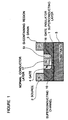
- FIG. 1 there is shown a diagrammatic sectional view of one embodiment of the superconducting device in accordance with the present invention.
- the shown superconducting device is a super-FET.
- the super-FET includes an oxide superconducting layer 1 formed on a substantially planar principal surface of a substrate 5.
- the oxide superconducting layer 1 has a gate electrode 4 embedded therein, and a substantially planar principal surface is formed of an upper surface of the oxide superconducting layer 1 itself and an upper exposed surface of the embedded gate electrode 4.
- An thickness of the oxide superconducting layer 1 is extremely thin underneath the gate electrode 4 so that a superconducting channel 10 having a thickness of about five nanometers is formed under the the gate electrode 4.
- the gate electrode 4 is formed of a gate insulator 16 formed directly on the superconducting channel 10, and a normal conductor layer 17 formed on the gate insulator 16.
- the normal conductor layer 17 is formed of for example polysilicon or a compound containing silicon, such as silicide.
- a portion of the oxide superconducting layer 1 surrouding the gate electrode 4 is changed into a region 51 containing silicon diffused from the normal conductor layer 17.
- the silicon containing region 51 is formed of a silicon doped oxide superconductor, which has a critical temperature greatly of remarkably lower than that of the other portion of the oxide superconducting layer 1. Alternately, the silicon containing region 51 no longer has superconductivity, dependently upon the doped amount of silicon. In any case, at an operating temperature of the shown super-FET, the oxide superconducting layer 1 is brought into and maintained in a superconducting condition, but the silicon containing region 51 does not have superconductivity. Accordingly, the gate electrode 4 is isolated from the oxide superconducting layer 1 by the the silicon containing region 51 and the gate isulator 16.
- a source electrode 2 and a drain electrode 3 are formed on the substantially planar principal surface of the oxide superconducting layer 1 at both sides of the gate electrode 4.
- a substrate 5 having a substantially planar principal surface is prepared as shown in Figure 2A.
- This substrate 5 is formed of for example, and insulating substrate such as a MgO (100) substrate, a SrTiO3 (100) substrate, a CdNdAlO4 (001) substrate or others, or a semiconductor substrate such as a silicon substrate having a principal surface coated with a buffer layer composed of an insulating film.
- the principal surface of the silicon substrate is continuously coated with MgAlO4 by a CVD (chemical vapor deposition) and also with BaTiO3 by a sputtering process.
- oxide superconductor thin film 11 is deposited on the principal surface of the substrate 5, by for example an off-axis sputtering, a reactive evaporation, an MBE (molecular beam epitaxy), a CVD, etc.
- This extremely thin oxide superconductor thin film 11 forms the superconducting channel when the super-FET is completed.
- the oxide superconductor material is preferably formed of, for example, a Y-Ba-Cu-O type compound oxide superconductor material, a Bi-Sr-Ca-Cu-O type compound oxide superconductor material, and a Tl-Ba-Ca-Cu-O type compound oxide superconductor material.
- a c -axis orientated thin film is preferably deposited, since the c -axis orientated thin film has a large critical current density in the direction in parallel to the substrate surface.
- an insulating layer 6 is deposited on the oxide superconductor thin film 11.
- the insulating layer 6 is deposited to have a thickness not less than ten nanometers.
- the insulating layer 6 is formed of an insulating material such as MgO, which does not form a large density of energy levels between the superconductor thin film 1 and the insulating layer 6.
- a polysilicon layer 7 is deposited on the insulating layer 6.
- This polysilicon layer 7 can be deposited by a vacuum evaporation of any other suitable process.
- the polysilicon layer 7 is 200 nm in thickness.
- the polysilicon layer 7 can be formed of a metal silicide in place of the polysilicon.
- the stacked layer of the insulating layer 6 and the polysilicon layer 7 is selectively removed so as to form the gate electrode 4.
- the polysilicon layer 7 is selectively etched so as remove all of the polysilicon layer excluding a portion which becomes the gate electrode on the superconducting channel 10, so that the normal conductor layer 17 of the gate electrode 4 is formed.
- the insulating layer 6 is selectively etched in a self alignment to the normal conductor layer 17 of the gate electrode 4, so that an gate insulator 16 is left on the superconducting channel 10 and only under the the normal conductor layer 17 of the gate electrode 4. In this connection, it is desired that the gate insulator 16 is side-etched in comparison with the normal conductor layer 17 of the gate electrode 4.
- the oxide superconductor thin film is grown again on the substrate 5, namely on the extremely thin oxide superconductor thin film 11, so that the gate electrode 4 is completely embedded within the deposited oxide superconductor thin film 1.
- the oxide superconductor thin film 1 is grown to have a thickness on the order of about 300 nm.
- the silicon of the polysilicon layer 17 of the gate electrode 4 is diffused into a portion of the oxide superconductor thin film 1 surrounding the gate electrode 4, so that a silicon containing region 51 is formed around the gate electrode 4.
- the silicon of the polysilicon layer 17 is not diffused into the oxide superconductor thin film 1 underneath the gate insulator 16, since the gate insulator 16 functions as a barrier preventing diffusion of the silicon of the polysilicon layer 17. Therefore, when the super-FET is cooled so that the oxide superconductor thin film 1 is brought into a superconducting condition, the gate electrode 4 is electrically isolated from the oxide superconductor thin film 1 by the silicon containing region 51 and the gate insulator 16.
- a photoresist layer (not shown) is deposited on the oxide superconductor thin film 1 in such a manner that the deposited photoresist layer has a flat upper surface, and then, the deposited photoresist layer and the deposited oxide superconductor thin film 1 are etched back, until the upper surface of the oxide superconductor thin film 1 is planarized and the polysilicon layer 17 of the gate electrode 4 is exposed at the planarized upper surface of the oxide superconductor thin film 1 as shown in Figure 2H.
- a source electrode 2 and a drain electrode 3 of Au are formed on the oxide superconductor thin film 1 at both sides of the gate electrode 4, respectively. With this, the super-FET in accordance with the present invention is completed.
- the super-FET in accordance with the present invention is manufactured in accordance with the method of the present invention, the limitation in the fine processing technique required for manufacturing the super-FET is relaxed.
- the upper surface of the superconductor thin film is planarized, it become easy to form conductor wirings in a later process. Accordingly, it is easy to manufacture the super-FET with good repeatability, and the manufactured super-FET has a stable performance.
- FIG 3 there is shown a diagrammatic perspective view of another embodiment of the superconducting device in accordance with the present invention.
- This second embodiment is a Josephson devise.
- the Josephson device includes a substrate 18, a pair of superconducting electrode zones 20A and 20B formed on the substrate 18 separately from each other, and a weak link zone 20C formed on the substrate between a pair of superconducting electrode zones 20A and 20B so as to couple the pair of superconducting electrode zones 20A and 20B.
- the shown device is formed of an oxide superconductor thin film 20, other then the substrate 18, and a barrier layer 22 and a diffusion material source layer 24 provided within the weak link zone 20C.
- the barrier layer 22 is formed separately from the substrate 18, and a diffusion material source layer 24 is formed directly on the barrier layer 22.
- the barrier layer 22 and the diffusion material source layer 24 are completely embedded in the oxide superconductor thin film 20.
- a diffusion material is diffused from the diffusion material source layer 24 into a portion 26 of the oxide superconductor thin film 20 above the diffusion material source layer 24, so that the portion 26 loses superconductivity. Namely, the portion 26 is an isolation region.
- the weak link zone 20C only a portion of the oxide superconductor thin film 20 under the barrier layer 22 has superconductivity.
- a pair of normal conductor electrodes 40A and 40B can be formed on the oxide superconductor thin film 20 in the superconducting electrode zones 20A and 20B, respectively.
- a Y-Ba-Cu-O type compound oxide superconductor material is used for forming the oxide superconductor thin film.
- the substrate 18 having a flat upper or principal surface is prepared as shown in Figure 4A.
- This substrate 18 is formed of an insulating substrate such as a MgO ( 100) substrate, a CdNdAlO4 (001) substrate or others. If these substrates are used, a c -axis orientated oxide superconductor thin film having a large critical current density in a direction in parallel to the substrate surface can be formed on the substrate.
- a first oxide superconductor thin film 28 is deposited on the substrate 10.
- This first oxide superconductor thin film 28 has an extremely thin thickness which is the same as that of a weak link region of a final or completed Josephson device so that the final or completed Josephson device has a desired characteristics.
- the thickness of the first oxide superconductor thin film 28 is not greater than 10 nm.
- the first oxide superconductor thin film 28 can be deposited, by for example an off-axis sputtering, a reactive evaporation, a CVD, etc.
- a barrier material layer 30 is deposited on the first oxide superconductor thin film 28.
- This barrier material layer 30 is formed of a metal such as Au and Pt which are stable to the oxide superconductor material.
- the barrier material layer 30 is preferably deposited by an electron beam evaporation.
- the barrier material layer 30 is preferably deposited by a vacuum evaporation.
- an Au thin film having a thickness not less than 25 nm is formed.
- a diffusion material layer 32 is deposited on the barrier material layer 30.
- This diffusion material layer 32 is preferably composed of a silicon or silicide thin film having a thickness not less than 25 nm, which can be deposited by an evaporation process or a CVD process.
- the diffusion material layer 32 and the barrier material layer 30 are patterned as shown in Figure 4E, so that the diffusion material layer 32 and the barrier material layer 30 are left in only a zone corresponding to a weak link region of the final or completed Josephson device, and the first oxide superconductor thin film 28 is exposed in the other zone.
- the width of the weak link region (the length of the weak link region in a direction of a superconduction current flowing through the weak link region) is 0.25 ⁇ m.
- This patterning is performed by a reactive ion etching using a resist for electron beam. In this connection, the etching condition is controlled or adjusted so that a side etching of the diffusion material layer 32 and the barrier material layer 30 are sufficiently promoted. With this etching, the width of the weak link region can be made narrower than that of a resist pattern.
- a second oxide superconductor thin film 20 is deposited on the substrate 10 on which the above mentioned various layers have been formed.
- the second oxide superconductor thin film 20 is epitaxially continuous to the first oxide superconductor thin film 28. Therefore, and integral oxide superconductor thin film is formed.
- a deposition surface is cleaned by a reverse sputtering before deposition of the second oxide superconductor thin film 20.
- the diffusion material contained in the diffusion material layer 24 or the material itself of the diffusion material layer 24 is diffused into the second oxide superconductor thin film 20 deposited on the diffusion material layer 24.
- crystalline growth of the oxide superconductor thin film 20 is impeded or prevented.
- the isolation region 26 losing the superconductivity is formed on the diffusion material layer 24, and therefore, the superconducting electrode zones 20A and 20B are confined separately from each other.
- the Josephson device thus formed has a substantially planar surface, but can be additionally planarized if necessary.
- the weak link is formed directly on the substrate, even if a planarization processing is executed, the characteristics of the Josephson device is subjected to no adverse effect.
- the silicon diffused region 51 is exaggeratingly depicted to extend not only on the upper surface of the polysilicon layer 17 but also on both side surfaces of the polysilicon layer 17, in the step shown in Figure 2G
- the isolation layer 26 is exaggeratingly depicted to extend only on the upper surface of the diffusion source layer 24 in Figure 4F.
- diffusion occurs in a lateral or sideward direction from the polysilicon layer 17 and the diffusion source layer 24.
- the diffusion source layer 24 does function as the conductor, it is sufficient if the portion above the diffusion source layer 24 is non-conductive so that a pair of superconducting electrode zones 20A and 20B can be coupled only through the weak link zone 20C.
- the VTB type Josephson device can operate when the barrier layer 22 and hence the weak link zone 20C are less than 1 ⁇ m. If the side diffusion is compared with the barrier layer 22 of about 0.25 ⁇ m in the shown embodiment, the amount or size of the side diffusion would be negligible.
- the super-FET since the gate electrode has to be completely isolated, the upper surface and both side surfaces of the polysilicon layer 17 have to be covered by the silicon diffused region 51 having a sufficient thickness to completely isolate the gate electrode.
- the super-FET can operate when the gate length is less than 0.1 ⁇ m. If the side diffusion is compared with the gate length of less than 0.1 ⁇ m, the amount or size of the side diffusion would never be negligible.
Description
- The present invention relates to a superconducting device and a method for manufacturing the same, and more specifically to a superconducting device including an oxide superconducting layer having a planar upper surface and a partially reduced thickness, and a method for manufacturing the same.
- Typical three-terminal devices which utilize a superconductor include a so called superconducting-base transistor and a so called super-FET (field effect transistor). The superconducting-base transistor includes an emitter of a superconductor or a normal conductor, a tunnel barrier of an insulator, a base of a superconductor, a semiconductor isolator and collector of a normal conductor, stacked in the named order. This superconducting-base transistor operates at a high speed and with a low power consumption, by utilizing high speed electrons passing through the tunnel barrier.
- The super-FET includes a semiconductor layer, and a ssuperconductor source electrode and a superconductor drain electrode which are formed closely to each other on the semiconductor layer. A portion of the semiconductor layer between the superconductor source electrode and the superconductor drain electrode has a greatly recessed or undercut rear surface so as to have a reduced thickness. In addition, a gate electrode is formed through a gate insulator layer on the recessed or undercut rear surface of the portion of the semiconductor layer between the superconductor source electrode and the superconductor drain electrode.
- A superconducting current flowing through the semiconductor layer portion between the superconductor source electrode and the superconductor drain electrode due to a superconducting proximity effect is controlled by an applied gate voltage. This super-FET also operates at a high speed with a low power consumption.
- In addition, in the prior art, there has been proposed a three-terminal superconducting device having a channel of a superconductor formed between a source electrode and a drain electrode, so that a current flowing through the superconducting channel is controlled by a voltage applied to a gate formed above the superconducting channel, such as described in the patent Application EP-A- 0 324 044.
- Both of the above mentioned superconducting-base transistor and the super-FET have a portion in which a semiconductor layer and a superconducting layer are stacked to each other. However, it is difficult to form a stacked structure of the semiconductor layer and the superconducting layer formed of an oxide superconductor which has been recently advanced in study. In addition, even if it is possible to form a stacked structure of the semiconductor layer and the oxide superconducting layer, it is difficult to control a boundary between the semiconductor layer and the oxide superconducting layer. Therefore, a satisfactory operation could not been obtained in these superconducting devices.
- In addition, since the super-FET utilizes the superconducting proximity effect, the superconductor source electrode and the superconductor drain electrode have to be located close to each other at a distance which is a few times the coherence length of the superconductor materials of the superconductor source electrode and the superconductor drain electrode. In particular, since an oxide superconductor has a short coherence length, if the superconductor source electrode and the superconductor drain electrode are formed of the oxide superconductor material, a distance between the superconductor source electrode and the superconductor drain electrode has to be on the order of a few ten nanometers. It is very difficult to conduct a fine processing such as a fine pattern etching so as to ensure the very short separation distance. Because of this, in the prior art, it has been impossible to manufacture the super-FET composed of the oxide superconductor material.
- Furthermore, it has been confirmed that the conventional three-terminal superconducting device having the superconducting channel shows a modulation operation. However, the conventional three-terminal superconducting device having the superconducting channel could not realize a complete ON/OFF operation, because a carrier density is too high. In this connection, since an oxide superconductor material has a low carrier density, it is expected to form a three-terminal superconducting device which has a superconducting channel and which can realize the complete ON/OFF operation, by forming the superconducting channel of the oxide superconducting material. In this connection, however, a thickness of the superconducting channel has to be made on the order of five nanometers.
- On the other hand, typical two-terminal devices which utilize a superconductor include a so called Josephson device, which comprises a pair of superconductors coupled to each other through a tunnel barrier. The Josephson device can realize a high speed switching.
- The Josephson device formed of an oxide superconductor material thin film can be realized in the form of a planer type, which is divided into a Dayem bridge (DMB) type and a variable thickness bridge (VTB) type.
- The Dayem bridge type Josephson device has been formed of a constant thickness oxide superconductor thin film which is formed on a subtrate and which is patterned in a plan view, so that a superconductor thin film region having a greatly narrow whidth is formed between a pair of superconductor thin film regions having a sufficient width. In other words, the pair of superconductor thin film regions having a sufficient width are coupled to each other by the superconductor thin film region having the greatly narrow width. Namely, a weak link of the Josephson junction in the superconductor thin film is formed at the greatly narrow width region.
- On the other hand, the variable thickness bridge type Josephson device has been formed of an oxide superconductor this film of a sufficient thickness which is formed on a substrate and which is partially etched or thinned in a thickness direction, so that a thinned oxide superconductor thin film portion is formed between a pair of superconductor thin film portions having the sufficient thickness. In other words, the pair of superconductor thin film portions having the sufficient thickness are coupled to each other by the thinned oxide superconductor thin film portion. Accordingly, a weak link of the Josephson junction is formed at the reduced thickness portion of the oxide superconductor thin film.
- As would be understood from the above, the characteristics of the planar type Josephson devices have a close relation to the width of the superconductor thin film region having the greatly narrow width in the Dayem bridge type Josephson device, and to the thickness of the thinned oxide superconductor thin film portion in the variable thickness bridge type Josephson device, both of which form the weak link of the Josephson junction. Therefore, in order to obtain desired characteristics with a good repeatability, a high precision on a sub-micron level of the processing such as the etching is required.
- The Dayem bridge type Josephson device can be said to be more preferable than the variable thickness bridge type Josephson device, since the Dayem bridge type Josephson device has a relatively planer surface, which is preferred in an integrated circuit. However, in order to form the weak link in the Dayem bridge type Josephson device, it is required to pattern an oxide superconductor thin film having the thickness on the order of 0.5µm to 1.0µm into a width of not greater the 0.2µm. However, it is very difficult to conduct this fine patterning with good repeatability.
- On the other hand, in the variable thickness bridge type Josephson device, the very fine pattering is not required in order to form the weak link. However, it is very difficult to uniformly control the remaining thickness of the thinned portion forming the weak link. In addition, the variable thickness bridge type Josephson device cannot have a satisfactorily planer surface. This is not preferable to the integrated circuit application.
- Moreover, the article "Novel method of patterning YBaCuO superconducting thin film", published in the Appl. Phys. Lett., vol.55, N° 9, pages 896-898, 28 August 1989, discloses that a thin film of silicon, deposited on a Mg0 substrate, will intermix with a deposited YBaCu0 film, so that it will inhibit the superconductivity after a rapid thermal annealing process. Owing to this phenomenon, micron-scale superconducting lines, with a critical temperature above 76K have been demonstrated.
- Accordingly, it is an object of the present invention to provide a superconducting device and a method for manufacturing the same, which have overcome the above mentioned defects of the conventional ones.
- Another object of the present invention is to provide an FET type superconducting device including an channel composed of an oxide superconducting layer having a planar upper surface and a partially reduced thickness, and a method for manufacturing the same with a good repeatability by using existing established processing techniques.
- Still another object of the present invention is to provide a Josephson junction superconducting device including a weak link composed of an oxide superconducting layer having a planar upper surface and a partially reduced thickness, and a method for manufacturing the same with a good repeatability by using existing established processing techniques.
- The above and other objects of the present invention are achieved in accordance with the present invention by a superconducting device which comprises a substrate having a principal flat surface, first and second oxide superconducting regions of a relatively thick thickness formed directly on the principal surface of the substrate separately from each other, and a third oxide superconducting region of an extremely thin thickness formed directly on the principal surface of the substrate between the first and second oxide superconducting regions so as to bridge the first and second oxide superconducting regions, a barrier layer of a non-superconductor material formed directly on the third oxide superconducting region, and a diffusion source layer of a non-superconductor material formed on the barrier layer, characterized in that it further comprises an isolation region formed to cover the upper surface or both side surfaces of the diffusion source layer, and in that the first, second and third oxide superconducting regions and the isolation region being formed of the same oxide superconductor material, the isolation region being diffused with the same material as at least one material contained in the diffusion source layer, so that when the first and second oxide superconducting regions are brought into a superconducting condition, the isolation region does not show superconductivity, and therefore, a superconducting current can flow between the first and second oxide superconducting regions through only the third oxide superconducting region.
- In a preferred embodiment, the oxide superconductor material is selected from the group consisting of a Y-Ba-Cu-O type compound oxide superconductor material, a Bi-Sr-Ca-Cu-O type compound oxide superconductor material, and a Tl-Ba-Ca-Cu-O type compound oxide superconductor material. In addition, the first, second and third oxide superconducting regions are formed of a single c-axis orientated single crystal film.
- The superconducting device in accordance with the present invention, the substrate, on which the oxide superconductor thin film is deposited, can be formed of an insulating substrate, preferably an oxide single crystalline substrate such as MgO, SrTiO₃, CdNdAlO₄, etc. These substrate materials are very effective in forming or growing a crystalline film having a high orientation property. However, the superconducting device can be formed on a semiconductor substrate if an appropriate buffer layer is deposited thereon. For example, the buffer layer on the semiconductor substrate can be formed of a double-layer coating formed of a MgAlO₄ layer and a BaTiO₃ layer if a silicon substrate is used.
- Preferably, the diffusion source layer is formed of a material selected from the group consisting of silicon and silicide, and the isolation region is diffuse with at least silicon. Furthermore, the barrier layer is formed of a material stable to the oxide superconductor material of the first, second and third oxide superconducting regions.
- In one embodiment, the isolation region is formed to cover at least the upper portion of the diffusion source layer. Preferably, the first and second oxide superconducting regions and the isolation region are formed of a single oxide superconductor thin film having a substantially planar surface. In this case, the third oxide superconducting region can form a weak link of a Josephson junction, and therefore, the superconducting device constitutes a Josepson device.
- In another embodiment, the isolation region is formed to cover at least both side surfaces of the diffusion source layer. In addition, the diffusion source layer can be formed of a conducting material and exposed so as to function as a gate electrode, and the isolation region can be formed of an insulating material. Preferably, the first and second oxide superconducting regions are formed of a single oxide superconductor thin film, and the first and second oxide superconducting regions and the diffusion source layer forming the gate electrode are formed to have a substantially planar surface. In this case, the superconducting device constitutes a super-FET, and the superconducting current flowing between the first and second electrodes through the third oxide superconducting region is controlled by a voltage applied to the gate electrode.
- As mentioned hereinbefore, in the conventional super-FET, a superconducting current flows through the semiconducting channel due to the superconducting proximity effect. However, in the super-FET in accordance with the present invention, a main current flows through the superconductor. Therefore, the limitation in the fine processing techniques required for manufacturing the super-FET can be relaxed.
- The above mentioned superconducting device in accordance with the present invention can be formed by preparing a substrate having a planar principal surface thereof, forming a first oxide superconductor thin film having a very thin thickness on the principal surface of the substrate, forming on a portion of the first oxide superconductor thin film a stacked structure including a barrier layer formed directly on the first oxide superconductor thin film and a diffusion source layer formed on the barrier layer, and growing a second oxide superconductor thin film on an exposed surface of the first oxide superconductor thin film until the stacked structure is embedded in the second oxide superconductor thin film, so that at least on material contained in the diffusion source layer is diffused into an region of the second oxide superconductor thin film surrounding the diffusion source layer, and the diffused region does not show superconductivity when a non-diffused region of the second oxide superconductor thin film shows superconductivity.
- As mentioned hereinbefore, in the conventional superconducting device, after the superconductor thin film having a uniform thickness and flat upper and lower surfaces was formed, the superconductor thin film is partially abraded or recessed in a thickness direction so as to form a thinned superconductor thin film portion which constitutes a superconducting channel in the super-FET and a weak link in the Josephson device. However, since the required thickness of the thinned superconductor thin film portion is very small, an extremely high degree of precision in a fine processing (for example, etching) has been required in order to obtain desired characteristics of the superconducting device.
- On the other hand, in the above mentioned method in accordance with the present invention, after a first superconductor thin film of an extremely thin thickness (which can constitute a superconducting channel in the super-FET and a weak link in the Josephson device) is formed to cover a whole of the principal surface of the substrate, a unique layered structure preventing a superconductor thin film growth is located on a portion of the first superconductor thin film, and then, a second superconductor thin film having a sufficient thickness is selectively grown on the first superconductor thin film. As result, the second superconductor thin film is continuously and epitaxially grown on the first superconductor thin film excluding the superconductor thin film growth preventing layered structure. On the other hand, the second superconductor thin film is not properly grown on the superconductor thin film growth preventing layered structure, and an insulative thin film is formed on the superconductor thin film growth preventing layered structure. Thus, portions of the second superconductor thin film at both sides of the superconductor thin film growth preventing layered structure is bridged by the first superconductor thin film of the extremely thin thickness under the superconductor thin film growth preventing layered structure. In the Josephson device, the first superconductor thin film of the extremely thin thickness forms a weak link, and the second superconductor thin film portions at both sides of the superconductor thin film growth preventing layered structure constitute a pair of superconducting electrode regions. On the other hand, in the super-FET, the first superconductor thin film of the extremely thin thickness forms a superconducting channel, and the second superconductor thin film portions at both sides of the superconductor thin film growth preventing layered structure constitute a pair of superconducting source/drain regions, respectively.
- The superconductor thin film growth preventing layered structure is constituted of a diffusion source layer contains a component which diffuses into the second superconductor thin film when the second superconductor thin film is deposited or grown on the first superconductor thin film, so that formation of a special crystal structure in the second superconductor thin film is prevented by the diffused or doped component. However, in order to prevent the diffusion component from being diffused into the first superconductor thin film, a barrier layer stable to the oxide superconductor material is sandwiched between the first superconductor thin film and the diffusion source layer.
- As seen from the above, the extremely thin oxide superconductor thin film (which can constitute a superconducting channel in the super-FET and a weak link in the Josephson device) can be easily formed by precisely controlling the deposition process, and therefore, with a high repeatability. Therefore, it is no longer necesary to conduct a high degree of fine processing such as a fine etching.
- In addition, since the upper surface of the superconductor thin film has a planarized upper surface, the superconducting device is very convenient in order to be assembled in an integrated circuit.
- In the super-FET, in order to ensure that the superconducting channel can be turned on and off by a voltage applied to the gate electrode, a thickness of the superconducting channel has to be on the order of five nanometers in the direction of an electric field created by the voltage applied to the gate electrode. This extremely thin superconducting channel can be easily realized or formed in accordance with the method of the present invention, since the superconducting channel is formed of the first oxide superconductor thin film portion which is deposited or grown to cover the whole of the substrate.
- For example, the first oxide superconductor thin film is formed to have the thickness on the order of about 5 nanometers. This extremely thin oxide superconductor thin film can be formed in a conventional process by precisely controlling both of the thin film growth speed and the growth time. For this purpose, a sputtering can be used. However, since the oxide superconductor crystal has a multi-layer structure in which respective constituent elements are stacked in a layered structured, it is possible to stack a desired number of unit cells of oxide superconductor, by using a MBE (molecular beam epitaxy).
- The extremely thin oxide superconductor thin film thus formed of deposited is very preferable in thickness to form a superconducting channel, but insufficient in thickness to form a source region and a drain region. Therefore, the superconducting layer in the source region and the drain region must be further thickened. The above mentioned method in accordance with the present invention is very effective in thickening the source region and the drain region while maintaining the thickness of the extremely thin oxide superconductor thin film in the superconducting channel zone. Namely, a gate electrode is formed on the extremely thin oxide superconductor thin film at a position corresponding to the superconducting channel, and the oxide superconductor thin film is deposited or grown again on the extremely thin oxide superconductor thin film, using the gate electrode as a mask. In this connection, it is preferred to perform this second deposition or growth of the oxide superconductor thin film until the gate electrode is completely embedded in the oxide superconductor thin film, and to planarize the oxide superconductor thin film until an upper surface of the gate electrode is exposed at the planarized upper surface of the oxide superconductor thin film.
- In the above mentioned process, the gate electrode is completely embedded in the oxide superconductor thin film at once. In the process of the second deposition or growth of the oxide superconductor thin film, the diffusion material such as silicon included in the gate electrode is diffused into a portion of the oxide superconductor thin film surrounding the gate electrode. Therefore, this diffusion material diffused region is formed to surround the gate electrode. The diffusion material diffused region has a lowered critical temperature or does not any longer have superconductivity, because of the diffuse impurity. Accordingly, when the super-FET is used at an operating temperature, this diffusion material diffused region functions as an insulator, and therefore, the gate electrode is electrically isolated from the oxide superconductor thin film by the gate insulator and the diffusion material diffused region.
- The above and other objects, features and advantages of the present invention will be apparent from the following description of preferred embodiments of the invention with reference to the accompanying drawings.
-
- Figure 1 is a diagrammatic sectional view of one embodiment of the superconducting device in accordance with the present invention;
- Figure 2A to 2I are diagrammatic sectional views for illustrating the process for manufacturing the superconducting device shown in Figure 1;
- Figure 3 is a diagrammatic perspective view of another embodiment of the superconducting device in accordance with the present invention; and
- Figure 4A to 4F are diagrammatic sectional views for illustrating the process for manufacturing the superconducting device shown in Figure 3.
- Referring to Figure 1, there is shown a diagrammatic sectional view of one embodiment of the superconducting device in accordance with the present invention. The shown superconducting device is a super-FET.
- The super-FET includes an
oxide superconducting layer 1 formed on a substantially planar principal surface of asubstrate 5. Theoxide superconducting layer 1 has agate electrode 4 embedded therein, and a substantially planar principal surface is formed of an upper surface of theoxide superconducting layer 1 itself and an upper exposed surface of the embeddedgate electrode 4. An thickness of theoxide superconducting layer 1 is extremely thin underneath thegate electrode 4 so that asuperconducting channel 10 having a thickness of about five nanometers is formed under the thegate electrode 4. Thegate electrode 4 is formed of agate insulator 16 formed directly on thesuperconducting channel 10, and anormal conductor layer 17 formed on thegate insulator 16. Thenormal conductor layer 17 is formed of for example polysilicon or a compound containing silicon, such as silicide. In addition, a portion of theoxide superconducting layer 1 surrouding thegate electrode 4 is changed into aregion 51 containing silicon diffused from thenormal conductor layer 17. - Therefore, the
silicon containing region 51 is formed of a silicon doped oxide superconductor, which has a critical temperature greatly of remarkably lower than that of the other portion of theoxide superconducting layer 1. Alternately, thesilicon containing region 51 no longer has superconductivity, dependently upon the doped amount of silicon. In any case, at an operating temperature of the shown super-FET, theoxide superconducting layer 1 is brought into and maintained in a superconducting condition, but thesilicon containing region 51 does not have superconductivity. Accordingly, thegate electrode 4 is isolated from theoxide superconducting layer 1 by the thesilicon containing region 51 and thegate isulator 16. - In addition, a
source electrode 2 and adrain electrode 3 are formed on the substantially planar principal surface of theoxide superconducting layer 1 at both sides of thegate electrode 4. - Now, the process for manufacturing the above mentioned superconducting device will be described with reference to Figure 2A to 2I.
- First, a
substrate 5 having a substantially planar principal surface is prepared as shown in Figure 2A. Thissubstrate 5 is formed of for example, and insulating substrate such as a MgO (100) substrate, a SrTiO₃ (100) substrate, a CdNdAlO₄ (001) substrate or others, or a semiconductor substrate such as a silicon substrate having a principal surface coated with a buffer layer composed of an insulating film. Preferably, the principal surface of the silicon substrate is continuously coated with MgAlO₄ by a CVD (chemical vapor deposition) and also with BaTiO₃ by a sputtering process. - As shown in figure 2B, and extremely thin oxide superconductor
thin film 11 on the order of about five nanometers is deposited on the principal surface of thesubstrate 5, by for example an off-axis sputtering, a reactive evaporation, an MBE (molecular beam epitaxy), a CVD, etc. This extremely thin oxide superconductorthin film 11 forms the superconducting channel when the super-FET is completed. The oxide superconductor material is preferably formed of, for example, a Y-Ba-Cu-O type compound oxide superconductor material, a Bi-Sr-Ca-Cu-O type compound oxide superconductor material, and a Tl-Ba-Ca-Cu-O type compound oxide superconductor material. In addition, a c-axis orientated thin film is preferably deposited, since the c-axis orientated thin film has a large critical current density in the direction in parallel to the substrate surface. - Then, as shown in Figure 2C, an insulating
layer 6 is deposited on the oxide superconductorthin film 11. The insulatinglayer 6 is deposited to have a thickness not less than ten nanometers. In addition, the insulatinglayer 6 is formed of an insulating material such as MgO, which does not form a large density of energy levels between the superconductorthin film 1 and the insulatinglayer 6. - Furthermore, as shown in Figure 2C, a
polysilicon layer 7 is deposited on the insulatinglayer 6. Thispolysilicon layer 7 can be deposited by a vacuum evaporation of any other suitable process. Thepolysilicon layer 7 is 200 nm in thickness. Thepolysilicon layer 7 can be formed of a metal silicide in place of the polysilicon. - Thereafter, the stacked layer of the insulating
layer 6 and thepolysilicon layer 7 is selectively removed so as to form thegate electrode 4. For this purpose, as shown in Figure 2E, thepolysilicon layer 7 is selectively etched so as remove all of the polysilicon layer excluding a portion which becomes the gate electrode on thesuperconducting channel 10, so that thenormal conductor layer 17 of thegate electrode 4 is formed. Then, as shown in Figure 2F, the insulatinglayer 6 is selectively etched in a self alignment to thenormal conductor layer 17 of thegate electrode 4, so that angate insulator 16 is left on thesuperconducting channel 10 and only under the thenormal conductor layer 17 of thegate electrode 4. In this connection, it is desired that thegate insulator 16 is side-etched in comparison with thenormal conductor layer 17 of thegate electrode 4. - After the
gate electrode 4 composed of thegate insulator 16 and thenormal conductor layer 17 of polysilicon is formed on thesuperconducting channel 10, as shown in Figure 2G, the oxide superconductor thin film is grown again on thesubstrate 5, namely on the extremely thin oxide superconductorthin film 11, so that thegate electrode 4 is completely embedded within the deposited oxide superconductorthin film 1. For example, the oxide superconductorthin film 1 is grown to have a thickness on the order of about 300 nm. - In the process of growth of the oxide superconductor
thin film 1, the silicon of thepolysilicon layer 17 of thegate electrode 4 is diffused into a portion of the oxide superconductorthin film 1 surrounding thegate electrode 4, so that asilicon containing region 51 is formed around thegate electrode 4. But, the silicon of thepolysilicon layer 17 is not diffused into the oxide superconductorthin film 1 underneath thegate insulator 16, since thegate insulator 16 functions as a barrier preventing diffusion of the silicon of thepolysilicon layer 17. Therefore, when the super-FET is cooled so that the oxide superconductorthin film 1 is brought into a superconducting condition, thegate electrode 4 is electrically isolated from the oxide superconductorthin film 1 by thesilicon containing region 51 and thegate insulator 16. - Thereafter, in order the planarize an upper surface of the deposited oxide superconductor
thin film 1, a photoresist layer (not shown) is deposited on the oxide superconductorthin film 1 in such a manner that the deposited photoresist layer has a flat upper surface, and then, the deposited photoresist layer and the deposited oxide superconductorthin film 1 are etched back, until the upper surface of the oxide superconductorthin film 1 is planarized and thepolysilicon layer 17 of thegate electrode 4 is exposed at the planarized upper surface of the oxide superconductorthin film 1 as shown in Figure 2H. - Finally, as shown in Figure 2I, a
source electrode 2 and adrain electrode 3 of Au are formed on the oxide superconductorthin film 1 at both sides of thegate electrode 4, respectively. With this, the super-FET in accordance with the present invention is completed. - As explained above, if the super-FET in accordance with the present invention is manufactured in accordance with the method of the present invention, the limitation in the fine processing technique required for manufacturing the super-FET is relaxed. In addition, since the upper surface of the superconductor thin film is planarized, it become easy to form conductor wirings in a later process. Accordingly, it is easy to manufacture the super-FET with good repeatability, and the manufactured super-FET has a stable performance.
- Referring to figure 3, there is shown a diagrammatic perspective view of another embodiment of the superconducting device in accordance with the present invention. This second embodiment is a Josephson devise.
- The Josephson device includes a
substrate 18, a pair ofsuperconducting electrode zones substrate 18 separately from each other, and aweak link zone 20C formed on the substrate between a pair ofsuperconducting electrode zones superconducting electrode zones - Here, the shown device is formed of an oxide superconductor
thin film 20, other then thesubstrate 18, and abarrier layer 22 and a diffusionmaterial source layer 24 provided within theweak link zone 20C. Thebarrier layer 22 is formed separately from thesubstrate 18, and a diffusionmaterial source layer 24 is formed directly on thebarrier layer 22. Thebarrier layer 22 and the diffusionmaterial source layer 24 are completely embedded in the oxide superconductorthin film 20. A diffusion material is diffused from the diffusionmaterial source layer 24 into aportion 26 of the oxide superconductorthin film 20 above the diffusionmaterial source layer 24, so that theportion 26 loses superconductivity. Namely, theportion 26 is an isolation region. As a result, in theweak link zone 20C, only a portion of the oxide superconductorthin film 20 under thebarrier layer 22 has superconductivity. In addition, a pair ofnormal conductor electrodes thin film 20 in thesuperconducting electrode zones - Now, the process for manufacturing the above mentioned superconducting device will be described with reference to Figure 4A to 4F. In the embodiment which will be described below, a Y-Ba-Cu-O type compound oxide superconductor material is used for forming the oxide superconductor thin film.
- First, the
substrate 18 having a flat upper or principal surface is prepared as shown in Figure 4A. Thissubstrate 18 is formed of an insulating substrate such as a MgO ( 100) substrate, a CdNdAlO₄ (001) substrate or others. If these substrates are used, a c-axis orientated oxide superconductor thin film having a large critical current density in a direction in parallel to the substrate surface can be formed on the substrate. - As shown in Figure 4B, a first oxide superconductor
thin film 28 is deposited on thesubstrate 10. This first oxide superconductorthin film 28 has an extremely thin thickness which is the same as that of a weak link region of a final or completed Josephson device so that the final or completed Josephson device has a desired characteristics. For example, the thickness of the first oxide superconductorthin film 28 is not greater than 10 nm. The first oxide superconductorthin film 28 can be deposited, by for example an off-axis sputtering, a reactive evaporation, a CVD, etc. In this example, the off-axis sputtering is performed under the condition that a sputtering gas is composed of Ar an O₂ at the rate of Ar : O₂ = 9 : 1, the sputtering gas pressure is 10 Pa, and the temperature is 700°C. - Then, as shown in Figure 4C, a
barrier material layer 30 is deposited on the first oxide superconductorthin film 28. Thisbarrier material layer 30 is formed of a metal such as Au and Pt which are stable to the oxide superconductor material. In the case of Pt being used, thebarrier material layer 30 is preferably deposited by an electron beam evaporation. In the case of Au being used, thebarrier material layer 30 is preferably deposited by a vacuum evaporation. In this example, an Au thin film having a thickness not less than 25 nm is formed. - Furthermore, as shown in Figure 4D, a diffusion material layer 32 is deposited on the
barrier material layer 30. This diffusion material layer 32 is preferably composed of a silicon or silicide thin film having a thickness not less than 25 nm, which can be deposited by an evaporation process or a CVD process. - Thereafter, the diffusion material layer 32 and the
barrier material layer 30 are patterned as shown in Figure 4E, so that the diffusion material layer 32 and thebarrier material layer 30 are left in only a zone corresponding to a weak link region of the final or completed Josephson device, and the first oxide superconductorthin film 28 is exposed in the other zone. In the shown example, the width of the weak link region (the length of the weak link region in a direction of a superconduction current flowing through the weak link region) is 0.25µm. This patterning is performed by a reactive ion etching using a resist for electron beam. In this connection, the etching condition is controlled or adjusted so that a side etching of the diffusion material layer 32 and thebarrier material layer 30 are sufficiently promoted. With this etching, the width of the weak link region can be made narrower than that of a resist pattern. - Thereafter, a second oxide superconductor
thin film 20 is deposited on thesubstrate 10 on which the above mentioned various layers have been formed. The second oxide superconductorthin film 20 is deposited by a conventional sputtering under the condition that a sputtering gas is composed of Ar and O₂ at the rate of Ar : O₂ = 9 : 1, the sputtering gas pressure is 10 Pa, and the temperature is 700°C. - In the process, in the
superconducting electrode zones thin film 28, the second oxide superconductorthin film 20 is epitaxially continuous to the first oxide superconductorthin film 28. Therefore, and integral oxide superconductor thin film is formed. Incidentally, for the purpose of elevating continuity between the first oxide superconductorthin film 28 and the second oxide superconductorthin film 20, it is preferred that a deposition surface is cleaned by a reverse sputtering before deposition of the second oxide superconductorthin film 20. - In this process of the deposition of the second oxide superconductor
thin film 20, on other hand, the diffusion material contained in thediffusion material layer 24 or the material itself of thediffusion material layer 24 is diffused into the second oxide superconductorthin film 20 deposited on thediffusion material layer 24. In other words, crystalline growth of the oxide superconductorthin film 20 is impeded or prevented. As a result, theisolation region 26 losing the superconductivity is formed on thediffusion material layer 24, and therefore, thesuperconducting electrode zones - The Josephson device thus formed has a substantially planar surface, but can be additionally planarized if necessary. In the Josephson device formed as mentioned above, since the weak link is formed directly on the substrate, even if a planarization processing is executed, the characteristics of the Josephson device is subjected to no adverse effect.
- Here, it should be noted that, in view of the function of the super-FET, the silicon diffused
region 51 is exaggeratingly depicted to extend not only on the upper surface of thepolysilicon layer 17 but also on both side surfaces of thepolysilicon layer 17, in the step shown in Figure 2G, and on the other hand, in view of the function of the VTB type Josephson device, theisolation layer 26 is exaggeratingly depicted to extend only on the upper surface of thediffusion source layer 24 in Figure 4F. In both of the process shown in Figure 2A to 2I and the process shown in Figure 4A to 4F, diffusion occurs in a lateral or sideward direction from thepolysilicon layer 17 and thediffusion source layer 24. However, in the VTB type Josephson device, since thediffusion source layer 24 does function as the conductor, it is sufficient if the portion above thediffusion source layer 24 is non-conductive so that a pair ofsuperconducting electrode zones weak link zone 20C. In addition, since the VTB type Josephson device can operate when thebarrier layer 22 and hence theweak link zone 20C are less than 1 µm. If the side diffusion is compared with thebarrier layer 22 of about 0.25 µm in the shown embodiment, the amount or size of the side diffusion would be negligible. On the other hand, in the super-FET, since the gate electrode has to be completely isolated, the upper surface and both side surfaces of thepolysilicon layer 17 have to be covered by the silicon diffusedregion 51 having a sufficient thickness to completely isolate the gate electrode. In addition, the super-FET can operate when the gate length is less than 0.1µm. If the side diffusion is compared with the gate length of less than 0.1µm, the amount or size of the side diffusion would never be negligible. - The invention has thus been shown and described with reference to the specific embodiments. However, it should be noted that the present invention is in no way limited to the details of the illustrate structures but changes and modifications may be made within the scope of the appended claims.
Claims (19)
- A superconducting device comprising a substrate (5, 18) having a principal flat surface, first and second oxide superconducting regions (1; 20A, 20B) of a relatively thick thickness formed directly on the principal surface of the substrate separately from each other, and a third oxide superconducting region (10, 20C) of an extremely thin thickness formed directly on the principal surface of the substrate between the first and second oxide superconducting regions so as to bridge the first and second oxide superconducting regions, a barrier layer (16, 22) of a non-superconductor material formed directly on the third oxide superconducting region, and a diffusion source layer (17, 24) of a non-superconductor material formed on the barrier layer, characterized in that it further comprises an isolation region (51, 26) formed to cover the upper surface or both side surfaces of the diffusion source layer, and in that the first, second and third oxide superconducting regions and the isolation region being formed of the same oxide superconductor material, the isolation region being diffused with the same material as at least one material contained in the diffusion source layer, so that when the first and second oxide superconducting regions are brought into a superconducting condition, the isolation region does not show superconductivity, and therefore, a superconducting current can flow between the first and second oxide superconducting regions through only the third oxide superconducting region.
- A superconducting device claimed in Claim 1 wherein at least the first and second oxide superconducting regions (1; 20A, 20B) and the isolation region (51, 26) are formed of a single oxide superconductor thin film having a substantially planar surface.
- A superconducting device claimed in Claim 2 wherein the oxide superconductor material is selected from the group consisting of a Y-Ba-Cu-O type compound oxide superconductor material, a Bi-Sr-Ca-Cu-O type compound oxide superconductor material, and a Tl-Ba-Ca-Cu-O type compound oxide superconductor material.
- A superconducting device claimed in Claim 3 wherein the first, second and third oxide superconducting regions (1, 20A, 20B, 10, 20C) are formed of a single c-axis orientated single crystal film.
- A superconducting device claimed in Claim 4 wherein the diffusion source layer (17, 24) is formed of a material selected from the group consisting of silicon and silicide, and the isolation region is diffused with at least silicon.
- A superconducting device claimed in Claim 5 wherein the barrier layer (16, 22) is formed of a material stable to the oxide superconductor material of the first, second and third oxide superconducting regions.
- A superconducting device claimed in Claim 5 wherein the substrate (5, 18) is formed of a material selected from the group consisting of a MgO (100) substrate, a SrTiO₃ (100) substrate and a CdNdAlO₄ (001) substrate, and a semiconductor substrate.
- A superconducting device claimed in Claim 5 wherein the substrate (5, 18) is formed of a semiconducting material substrate and a principal surface of the semiconducting material substrate is coated with an insulating material layer which is formed of a MgAlO₄ layer and a BaTiO₃ layer.
- A superconducting device claimed in Claim 1 wherein the isolation region (51, 26) is formed to cover at least the upper portion of the diffusion source layer and the third oxide superconducting region has a thickness of not greater than 10 nm and forms a weak link of a Josephson junction, so that the superconducting device constitutes a Josephson device.
- A superconducting device claimed in Claim 9 wherein the barrier layer (16, 22) is formed of a metal stable to the oxide superconductor material of the first, second and third oxide superconducting regions.
- A superconducting device claimed in Claim 10 wherein the metal is selected from the group consisting of Au and Pt.
- A superconducting device claimed in Claim 1 further including a first electrode formed on the first oxide superconducting region (1, 20A) and a second electrode formed on the second oxide superconducting region (1, 20 B), so that a superconducting current can flow between the first and second electrodes through the third oxide superconducting region.
- A superconducting device claimed in Claim 12 wherein the diffusion source layer (17, 24) is formed of a conducting material and exposed so as to function as a gate electrode, and the isolation region (51, 26) is formed of an insulating material, so that the superconducting device constitutes a super-FET, and the superconducting current flowing between the first and second electrodes through the third oxide superconducting region (10, 20C) is controlled by a voltage applied to the gate electrode.
- A superconducting device claimed in Claim 13 wherein each of the first and second electrodes and the gate electrode is formed of a superconductor material or a normal conductor material.
- A superconducting device claimed in Claim 13 wherein the isolation region (51, 26) is formed of an insulating material which does not form a large density of energy levels between the oxide superconductor material of the third oxide superconducting region and the insulating material of the isolation region.
- A superconducting device claimed in Claim 15 wherein the third oxide superconducting region (10, 20C) has a thickness of about 5 nm and the barrier layer is formed of MgO and has a thickness of not less than 10 nanometers.
- A method of manufacturing a superconducting device, comprising the step of preparing a substrate (5,18) having a planar principal surface thereof, forming a first oxide superconductor thin film having a very thin thickness on the principal surface of the substrate, forming on a portion of the first oxide superconductor thin film a stacked structure including a barrier layer (16, 22) formed directly on the first oxide superconductor thin film and a diffusion source layer (17, 24) formed on the barrier layer, and growing a second oxide superconductor thin film on an exposed surface of the first oxide superconductor thin film until the stacked structure is embedded in the second oxide superconductor thin film, so that at least one material contained in the diffusion source layer is diffused into an region of the second oxide superconductor thin film surrounding the diffusion source layer, and the diffused region does not show superconductivity when a non-diffused region of the second oxide superconductor thin film shows superconductivity.
- A method claimed in Claim 17 wherein after formation of the second oxide superconductor thin film, a resist layer is coated on the second oxide superconductor thin film so as to have a flat upper surface, and the resist layer and the second oxide superconductor thin film are etched back until the oxide superconductor thin film has the planar upper surface.
- A method claimed in Claim 18 wherein the the second oxide superconductor thin film is etched back until the diffusion source layer is exposed.
Applications Claiming Priority (4)
| Application Number | Priority Date | Filing Date | Title |
|---|---|---|---|
| JP2239423A JPH04118978A (en) | 1990-09-10 | 1990-09-10 | Superconducting element and manufacture thereof |
| JP239423/90 | 1990-09-10 | ||
| JP2257853A JP2597745B2 (en) | 1990-09-27 | 1990-09-27 | Superconducting element and fabrication method |
| JP257853/90 | 1990-09-27 |
Publications (3)
| Publication Number | Publication Date |
|---|---|
| EP0475838A2 EP0475838A2 (en) | 1992-03-18 |
| EP0475838A3 EP0475838A3 (en) | 1992-07-08 |
| EP0475838B1 true EP0475838B1 (en) | 1996-03-06 |
Family
ID=26534242
Family Applications (1)
| Application Number | Title | Priority Date | Filing Date |
|---|---|---|---|
| EP91402409A Expired - Lifetime EP0475838B1 (en) | 1990-09-10 | 1991-09-10 | Superconducting device having a reduced thickness of oxide superconducting layer and method for manufacturing the same |
Country Status (4)
| Country | Link |
|---|---|
| US (2) | US5621223A (en) |
| EP (1) | EP0475838B1 (en) |
| CA (1) | CA2051048C (en) |
| DE (1) | DE69117628T2 (en) |
Families Citing this family (10)
| Publication number | Priority date | Publication date | Assignee | Title |
|---|---|---|---|---|
| CA2051778C (en) * | 1990-09-19 | 1997-05-06 | Takao Nakamura | Method for manufacturing superconducting device having a reduced thickness of oxide superconducting layer and superconducting device manufactured thereby |
| CA2085290C (en) * | 1991-12-13 | 1997-08-05 | Takao Nakamura | Superconducting device having an extremely thin superconducting channel formed of oxide superconductor material and method for manufacturing the same |
| JPH05291637A (en) * | 1992-04-09 | 1993-11-05 | Sumitomo Electric Ind Ltd | Superconductive field effect type element |
| US5552374A (en) * | 1992-04-09 | 1996-09-03 | Sumitomo Electric Industries, Ltd. | Oxide superconducting a transistor in crank-shaped configuration |
| CN100483651C (en) * | 1992-08-27 | 2009-04-29 | 株式会社半导体能源研究所 | Process for fabricating semiconductor device |
| US9741918B2 (en) | 2013-10-07 | 2017-08-22 | Hypres, Inc. | Method for increasing the integration level of superconducting electronics circuits, and a resulting circuit |
| US10763420B2 (en) | 2016-06-13 | 2020-09-01 | Intel Corporation | Josephson Junction damascene fabrication |
| EP3505490B1 (en) * | 2017-12-29 | 2022-02-09 | Imec Vzw | A method for forming a qubit device |
| WO2019173448A1 (en) * | 2018-03-06 | 2019-09-12 | Cornell University | Epitaxial semiconductor/superconductor heterostructures |
| FR3116946B1 (en) * | 2020-11-27 | 2022-11-11 | Commissariat Energie Atomique | Method for making a quantum device |
Family Cites Families (10)
| Publication number | Priority date | Publication date | Assignee | Title |
|---|---|---|---|---|
| KR910002311B1 (en) * | 1987-02-27 | 1991-04-11 | 가부시기가이샤 히다찌세이사꾸쇼 | A superconductor device |
| JPH0634418B2 (en) * | 1987-09-07 | 1994-05-02 | 株式会社半導体エネルギー研究所 | Method for manufacturing superconducting element |
| JPS646964A (en) * | 1987-06-29 | 1989-01-11 | Fuji Photo Film Co Ltd | Capsule toner |
| DE3876228T2 (en) * | 1988-01-15 | 1993-06-03 | Ibm | FIELD EFFECT ARRANGEMENT WITH SUPRAL-CONDUCTING CHANNEL. |
| JP2862137B2 (en) * | 1988-08-11 | 1999-02-24 | 古河電気工業株式会社 | Superconducting transistor |
| JP3015408B2 (en) * | 1989-05-23 | 2000-03-06 | 三洋電機株式会社 | Method for manufacturing superconducting transistor |
| JPH0354875A (en) * | 1989-07-24 | 1991-03-08 | Furukawa Electric Co Ltd:The | Formation of superconductor circuit |
| US5229360A (en) * | 1989-07-24 | 1993-07-20 | The Furukawa Electric Co., Ltd. | Method for forming a multilayer superconducting circuit |
| JPH0355889A (en) * | 1989-07-25 | 1991-03-11 | Furukawa Electric Co Ltd:The | Manufacture of superconducting multilayered circuit |
| CA2051778C (en) * | 1990-09-19 | 1997-05-06 | Takao Nakamura | Method for manufacturing superconducting device having a reduced thickness of oxide superconducting layer and superconducting device manufactured thereby |
-
1991
- 1991-09-10 DE DE69117628T patent/DE69117628T2/en not_active Expired - Fee Related
- 1991-09-10 CA CA002051048A patent/CA2051048C/en not_active Expired - Fee Related
- 1991-09-10 EP EP91402409A patent/EP0475838B1/en not_active Expired - Lifetime
-
1995
- 1995-08-16 US US08/515,701 patent/US5621223A/en not_active Expired - Fee Related
-
1997
- 1997-01-02 US US08/778,370 patent/US5739084A/en not_active Expired - Fee Related
Also Published As
| Publication number | Publication date |
|---|---|
| US5739084A (en) | 1998-04-14 |
| DE69117628D1 (en) | 1996-04-11 |
| DE69117628T2 (en) | 1996-09-26 |
| CA2051048A1 (en) | 1992-03-11 |
| EP0475838A2 (en) | 1992-03-18 |
| CA2051048C (en) | 1996-07-02 |
| US5621223A (en) | 1997-04-15 |
| EP0475838A3 (en) | 1992-07-08 |
Similar Documents
| Publication | Publication Date | Title |
|---|---|---|
| EP0480814B1 (en) | Superconducting device having an extremely thin superconducting channel formed of oxide superconductor material and method for manufacturing the same | |
| EP0478465B1 (en) | Method for manufacturing superconducting device having a reduced thickness of oxide superconducting layer and superconducting device manufactured thereby | |
| EP0484253B1 (en) | Superconducting device having an extremely thin superconducting channel formed of oxide superconductor material and method for manufacturing the same | |
| US5494891A (en) | Method for manufacturing three-terminal oxide superconducting devices | |
| EP0475838B1 (en) | Superconducting device having a reduced thickness of oxide superconducting layer and method for manufacturing the same | |
| US5717222A (en) | Superconducting device having an extremely thin superconducting channel formed of oxide superconductor material and method for manufacturing the same | |
| EP0477103B1 (en) | Method for manufacturing superconducting device having a reduced thickness of oxide superconducting layer and superconducting device manufactured thereby | |
| EP0477063B1 (en) | Superconducting device having a reduced thickness of oxide superconducting layer and method for manufacturing the same | |
| US5637555A (en) | Method for manufacturing a three-terminal superconducting device having an extremely short superconducting channel | |
| US5854493A (en) | Superconduting device having an extremely short superconducting channel formed of oxide superconductor material and method for manufacturing the same | |
| EP0488837B1 (en) | Method for manufacturing superconducting device having a reduced thickness of oxide superconducting layer and superconducting device manufactured thereby | |
| EP0534811A2 (en) | Method of manufacturing superconducting thin film formed of oxide superconductor having non superconducting region in it, and method of manufacturing superconducting device utilizing the superconducting thin film | |
| EP0478463B1 (en) | Superconducting device having an extremely thin superconducting channel formed of oxide superconductor material | |
| EP0557207B1 (en) | Josephson junction device of oxide superconductor and process for preparing the same | |
| JP2738144B2 (en) | Superconducting element and fabrication method | |
| EP0790655B1 (en) | Superconducting field effect device having a superconducting channel and method for manufacturing the same | |
| JP2597745B2 (en) | Superconducting element and fabrication method | |
| CA2243654A1 (en) | Superconducting field effect device having a superconducting channel and method for manufacturing the same |
Legal Events
| Date | Code | Title | Description |
|---|---|---|---|
| PUAI | Public reference made under article 153(3) epc to a published international application that has entered the european phase |
Free format text: ORIGINAL CODE: 0009012 |
|
| AK | Designated contracting states |
Kind code of ref document: A2 Designated state(s): DE FR GB |
|
| PUAL | Search report despatched |
Free format text: ORIGINAL CODE: 0009013 |
|
| AK | Designated contracting states |
Kind code of ref document: A3 Designated state(s): DE FR GB |
|
| 17P | Request for examination filed |
Effective date: 19920722 |
|
| 17Q | First examination report despatched |
Effective date: 19940719 |
|
| GRAA | (expected) grant |
Free format text: ORIGINAL CODE: 0009210 |
|
| AK | Designated contracting states |
Kind code of ref document: B1 Designated state(s): DE FR GB |
|
| REF | Corresponds to: |
Ref document number: 69117628 Country of ref document: DE Date of ref document: 19960411 |
|
| ET | Fr: translation filed | ||
| PLBE | No opposition filed within time limit |
Free format text: ORIGINAL CODE: 0009261 |
|
| STAA | Information on the status of an ep patent application or granted ep patent |
Free format text: STATUS: NO OPPOSITION FILED WITHIN TIME LIMIT |
|
| 26N | No opposition filed | ||
| PGFP | Annual fee paid to national office [announced via postgrant information from national office to epo] |
Ref country code: FR Payment date: 19980909 Year of fee payment: 8 |
|
| PGFP | Annual fee paid to national office [announced via postgrant information from national office to epo] |
Ref country code: DE Payment date: 19980921 Year of fee payment: 8 |
|
| PGFP | Annual fee paid to national office [announced via postgrant information from national office to epo] |
Ref country code: GB Payment date: 19981001 Year of fee payment: 8 |
|
| PG25 | Lapsed in a contracting state [announced via postgrant information from national office to epo] |
Ref country code: GB Free format text: LAPSE BECAUSE OF NON-PAYMENT OF DUE FEES Effective date: 19990910 |
|
| GBPC | Gb: european patent ceased through non-payment of renewal fee |
Effective date: 19990910 |
|
| PG25 | Lapsed in a contracting state [announced via postgrant information from national office to epo] |
Ref country code: FR Free format text: LAPSE BECAUSE OF NON-PAYMENT OF DUE FEES Effective date: 20000531 |
|
| PG25 | Lapsed in a contracting state [announced via postgrant information from national office to epo] |
Ref country code: DE Free format text: LAPSE BECAUSE OF NON-PAYMENT OF DUE FEES Effective date: 20000701 |
|
| REG | Reference to a national code |
Ref country code: FR Ref legal event code: ST |