EP0473277A2 - Apparatus for controlling access to a data bus - Google Patents
Apparatus for controlling access to a data bus Download PDFInfo
- Publication number
- EP0473277A2 EP0473277A2 EP91306702A EP91306702A EP0473277A2 EP 0473277 A2 EP0473277 A2 EP 0473277A2 EP 91306702 A EP91306702 A EP 91306702A EP 91306702 A EP91306702 A EP 91306702A EP 0473277 A2 EP0473277 A2 EP 0473277A2
- Authority
- EP
- European Patent Office
- Prior art keywords
- data bus
- processing unit
- host
- bus
- computing system
- Prior art date
- Legal status (The legal status is an assumption and is not a legal conclusion. Google has not performed a legal analysis and makes no representation as to the accuracy of the status listed.)
- Granted
Links
Images


Classifications
-
- G—PHYSICS
- G06—COMPUTING; CALCULATING OR COUNTING
- G06F—ELECTRIC DIGITAL DATA PROCESSING
- G06F13/00—Interconnection of, or transfer of information or other signals between, memories, input/output devices or central processing units
- G06F13/38—Information transfer, e.g. on bus
- G06F13/40—Bus structure
- G06F13/4004—Coupling between buses
- G06F13/4027—Coupling between buses using bus bridges
-
- G—PHYSICS
- G06—COMPUTING; CALCULATING OR COUNTING
- G06F—ELECTRIC DIGITAL DATA PROCESSING
- G06F13/00—Interconnection of, or transfer of information or other signals between, memories, input/output devices or central processing units
- G06F13/14—Handling requests for interconnection or transfer
Definitions
- the present invention is directed to an apparatus for use with a host computing system for controlling access to a first data bus, which first data bus is external of the host computing system.
- the first data bus is operatively connected to a second data bus which is internal of the host computing system.
- the present invention is directed to an apparatus commonly known as a bus master circuit used in controlling access to a system bus associated with a host computing system.
- bus master circuit As an integral part of a computer processing unit which may be utilized either as a host computer processing unit or as a bus master control local computer processing unit.
- the mode in which the particular processing unit is employed is determined by setting bits in a register to enable or disable the bus master support circuit portion of the processing unit architecture.
- bus master support circuit integrally within the design of a computer processing unit, the costs of integration already incorporated for design and manufacture of the computer processing unit are spread across additional applications for which the unit may be utilized. That is, the marginal increase in design and integration cost to incorporate the bus master support circuit of the present invention is minimal in comparison with similar design and integration costs which would be incurred for a wholly separate bus master support circuit.
- a computer processing unit configured to operate as a bus master local processing unit has additional intelligent processing capability not generally found nor economically designed into prior art bus master circuits.
- an apparatus for use with a host computing system for controlling access to a first data bus which is external of the host computing system, which first data bus is operatively connected with a second data bus internal of the host computing system.
- the apparatus comprises a local processing unit which is configured substantially the same as the host processing unit and is driven by a separate local program distinct from the host processing program driving the host processing unit.
- the apparatus further comprises a supplemental processing circuit for processing information, which supplemental processing circuit is responsive to the host processing unit and to the local processing unit to determine whether the host processing unit or the local processing unit has operative access to the first data bus.
- the supplemental processing circuit is integrally configured with the local processing unit, and the first data bus and the second data bus are operatively connected by a configurable buffer circuit for effecting data bus connection. Further, in the preferred embodiment of the present invention, the supplemental processing circuit generates an intervention signal in response to the host processing unit or to the local processing unit, the buffer circuit responding to the intervention signal by configuring appropriately to provide operative access by the apparatus to the second data bus.
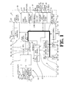
- Apparatus 10 is illustrated as situated on a single substrate 12.
- Apparatus 10 includes a computer processing unit 14, a connection 16 for an S-bus (not shown) and supportive peripheral devices 18 comprising an S-bus interface circuit 20 and a bus master support circuit 22.
- S-bus supportive peripheral devices 18 are preferably configured to accommodate direct connection of an S-bus to apparatus 10 with no additional peripheral devices required for an effective operative connection.
- a connection 24 for an M-bus (not shown) has associated therewith M-bus supportive peripheral devices 26, including a dynamic random access memory (DRAM) control unit 28 and a shadow random access memory (RAM) control unit 30.
- M-bus supportive peripheral devices 26 are configured to allow direct connection of the M-bus to M-bus connection 24 with no additional supportive peripheral devices required for an effective operative connection.
- a connection 32 with an X-bus (not shown) is also provided for apparatus 10.
- X-bus supportive peripheral devices 34 Associated with X-bus connection 32 are X-bus supportive peripheral devices 34, including an X-bus interface 36.
- X-bus supportive peripheral devices 34 are preferably configured to allow direct connection of the X-bus to X-bus connection 32 with no additional peripheral devices required for an effective operative connection.
- the S-bus is intended for use as a system-expansion bus to which would be connected industry-standard signal generators, timing devices, and other expansion cards and subsystems.
- the M-bus is used for communication to direct DRAM interfaces
- the X-bus is employed as an expansion bus to effect connection with such devices as read-only memories (ROMs), keyboard controllers, numeric co-processors, and the like.
- Apparatus 10 further comprises a plurality of core pripheral devices 38 which include, by way of example, a direct memory access (DMA) unit 40, an interrupt unit 42, a counter/timer device 44, and a real time clock and static RAM device 46.
- the various core peripheral devices 38 are operatively connected to input-output pins in order to perform their intended function.
- DMA unit 40 is operatively connected with input-output pins 48 in order to receive data request signals (DREQ) and transmit data acknowledgement signals (DACK)
- interrupt unit 42 is operatively connected with input-output pins 50 in order to receive interrupt signals (Ints)
- counter/timer device 44 is operatively connected with input-output pins 52 to provide operative connection with a system speaker (Spkr)
- real time clock and static RAM device 46 is operatively connected to input-output pins 54 in order to receive power from a power supply, such as VBatt.
- ROMs and keyboard controllers are connectable to apparatus 10 X-bus connection 32
- the preferred embodiment of apparatus 10 illustrated in Fig. 1 also provides,for direct ROM connection to a ROM interface 56 through an input-output pins 58.
- a keyboard interface 60 is also provided for access to apparatus 10 via input-output pins 62.
- additional supportive peripheral devices 64 including a co-processor interface 66, a reset circuit 68, a power control circuit 70, and a clock multiplexer and divider unit 72.
- Input-output pins are provided for access to the various additional supportive peripheral devices 64 so that co-processor interface 66 is connected with input-output pins 74, reset circuit 68 is connected with input-output pins 76, and clock multiplexer divider unit 72 is connected with a plurality of input-output pins 78.
- An internal bus 80 is provided to effect communications among the various components of apparatus 10, including S-bus supportive peripheral devices 18, M-bus supportive peripheral devices 26, X-bus supportive peripheral devices 34, core peripheral devices 38, and computer processing unit 14.
- Computer processing unit (CPU) 14 is operatively connected with internal bus 80 via memory management unit (MMU) 82 and its associated address latch 84 and data buffer 86.
- MMU memory management unit
- Computer processing unit 14 is responsive to a CPU control device 88, which CPU control device 88 is in intimate communicational relation with a bus control device 90.
- Bus control device 90 is operatively connected with internal bus 80 and includes a refresh generator 92 which is responsive to counter/timer 44 to periodically refresh specified components of apparatus 10, such as dynamic RAMs (DRAMs) through DRAM control unit 28.
- DRAMs dynamic RAMs
- Internal supportive peripheral devices 94 are situated intermediate internal bus 80 and bus control circuit 90, including a non-maskable interface (NMI) port 96, an input-output decode circuit 98, and configurable registers 100.
- NMI non-maskable interface
- apparatus 10 provides appropriate bus-accomodating means such as S-bus supportive peripheral devices 18, M-bus supportive peripheral devices 26, and X-bus supportive peripheral devices 34, as well as ROM interface 56 and keyboard interface 60, to support direct connection of peripheral devices via data buses to apparatus 10 with no additional supportive peripheral devices required.
- Effective and efficient internal communications within apparatus 10 are provided by internal bus 80, access to which is controlled by bus control circuit 90 so that computer processing unit 14 may provide information to or receive information from any of the several supportive external buses via internal bus 80. Further, information may be exchanged among the various external buses according to bus control circuit 90, as dictated by the program driving computer processing unit 14, all via internal bus 80.
- apparatus 10 is configured on a single substrate 12 as an integrated digital circuit, thereby providing the advantages of higher operating speed, lower power consumption, and reduced occupancy of "real estate" in its physical embodiment.
- Fig. 2 is a schematic perspective drawing illustrating the employment of the present invention with a host computing system.
- a host processing system 10 including a computer processing unit 14, is carried with associated devices 15 on a substrate 12.
- the apparatus 210 of the present invention is carried on a substrate 212. Also carried on substrate 212 are additional devices in support of apparatus 210, such as erasable programmable memories (EPROMs) 214, dynamic random access memories (DRAMs) 216, and peripherals 218, 219.
- EPROMs erasable programmable memories
- DRAMs dynamic random access memories
- EPROM 214 and peripherals 218, 219 are associated with X'-bus 220;
- DRAMs 216 are associated with M'-bus 222;
- S'-bus 224 is operatively connected with apparatus 10 at its S-bus interface 20 (see Fig. 1), not shown in detail in Fig. 2.
- S'-bus 224 is connected to S-bus 16 (see Fig. 1).
- Fig. 3 is a schematic diagram of the preferred embodiment of the present invention.
- a bus master support circuit 22 is illustrated.
- Apparatus 22 is comprised of a page register 230 which receives address information from internal data bus 80 (not shown) at bus connector 232, and receives read/write control information at input 234.
- Page register 230 produces an address page output signal at output 236 and applies that signal at an input 238 to a memory hit compara device 240, as well as at an input 242 to an input-output hit compare unit 244.
- Address information relating to memory operations which is identified by the particular address bits provided, is provided as input 246 to memory hit compare unit 240.
- address information relating to input-output operations is applied as input 248 of input-output hit compare unit 244.
- one of the memory hit compare unit 240 and input-output hit compare unit 244 will produce an output indicating a "hit", i.e., an equality of comparison of address page output signal from page register 230 and address information received at input 246 or input 248.
- output 250 from input-output hit compare unit 244 or output 252 from memory hit compare unit 240 will be positive, but not both.
- Outputs 250, 252 are applied as inputs to hit detect unit 254.
- Bus master support apparatus 22 also includes a control register 260 for receiving information from internal data bus 80 (not shown) at bus connector 262 and for receiving read-write signals at input 264.
- Control register 260 has a number of outputs, including data type indicators HIE at output 266 and HME at output 268.
- page register 230 and control register 260 cooperate whereby page register 230 sets a window address by its address page output signal 236 and control register 260 sets a window type: input-output type operation (output signal HIE 266); or memory-type operation, (output signal HME 268).
- signal HIE is provided at input 270 and signal HME is provided at input 272 of hit detect unit 254.
- hit detect unit 254 ascertains the window address as well as window type associated with a given operation by receiving inputs 250, 252, 270, 272.
- Local computer processing unit status is provided to detect unit 254 at bus connector 274. Additional outputs of control register 260 are also applied as inputs to hit detect unit 254: acquire bus output 276 from control register 260 is applied to control and status unit 294 to request access to S-bus 16 (Fig. 1); signal BCON at output 280 of control register 260 and signal BMM at output 282 of control register 260 control whether bus master support circuit 22 is engaged or not engaged. Signal BMM is applied as input 284 of hit detect unit 254. Input 278 provides an indication to hit detect unit 254 when S-bus 16 (Fig. 1) is acquired.
- Control and status unit 294 is a programmable logic unit responsive to its various inputs, which include outputs 276, 280, 282 from control register 260 and output 292 from hit detect unit 254 to produce outputs responsive to those various inputs according to a program in either the form of pin signals 296 or the form of an intervention signal at output 298.
- Pin signals 296 relate to communicating to the host computer processing unit to take control of the host computer processing unit's internal bus and comprise a bus request signal 300 which is issued by control and status unit 294 when it is desired that bus matter support circuit 22 take control of S-bus interface 20 of the host computing system (not shown).
- the host computing system indicates that such control by bus master support unit 22 will be allowed by issuing a bus acknowledge signal which is received by control and status unit 294 at input 302. Once a bus acknowledge signal is received at input 302, and enabling signal is passed on control line 304 to S-bus interface 20 (Fig. 1) to enable data transfer on S-bus 16 (Fig. 1).
- An intervention signal 298 is produced by control and status unit 294 when it is desired to take control of S-bus interface 20 of a host device and, in such case, intervention signal 298 is applied to S-bus buffer control unit 308 in order to modify normal buffer control signals received from bus control unit 90 (not shown) on bus connector 310 to produce modified buffer control signals to S-bus interface 20 on output bus connector 312.
Landscapes
- Engineering & Computer Science (AREA)
- Theoretical Computer Science (AREA)
- General Engineering & Computer Science (AREA)
- Physics & Mathematics (AREA)
- General Physics & Mathematics (AREA)
- Computer Hardware Design (AREA)
- Bus Control (AREA)
- Multi Processors (AREA)
- Selective Calling Equipment (AREA)
Abstract
Description
- The present invention is directed to an apparatus for use with a host computing system for controlling access to a first data bus, which first data bus is external of the host computing system. The first data bus is operatively connected to a second data bus which is internal of the host computing system. Specifically, the present invention is directed to an apparatus commonly known as a bus master circuit used in controlling access to a system bus associated with a host computing system.
- Of particular interest in connection with the present invention is the structure of the bus master circuit as an integral part of a computer processing unit which may be utilized either as a host computer processing unit or as a bus master control local computer processing unit. The mode in which the particular processing unit is employed is determined by setting bits in a register to enable or disable the bus master support circuit portion of the processing unit architecture.
- By such incorporation of a bus master support circuit integrally within the design of a computer processing unit, the costs of integration already incorporated for design and manufacture of the computer processing unit are spread across additional applications for which the unit may be utilized. That is, the marginal increase in design and integration cost to incorporate the bus master support circuit of the present invention is minimal in comparison with similar design and integration costs which would be incurred for a wholly separate bus master support circuit.
- Further, by employing an integrated system design approach, a computer processing unit configured to operate as a bus master local processing unit has additional intelligent processing capability not generally found nor economically designed into prior art bus master circuits.
- Accordingly, we describe an apparatus for use with a host computing system for controlling access to a first data bus which is external of the host computing system, which first data bus is operatively connected with a second data bus internal of the host computing system. The apparatus comprises a local processing unit which is configured substantially the same as the host processing unit and is driven by a separate local program distinct from the host processing program driving the host processing unit. The apparatus further comprises a supplemental processing circuit for processing information, which supplemental processing circuit is responsive to the host processing unit and to the local processing unit to determine whether the host processing unit or the local processing unit has operative access to the first data bus.
- Preferably, the supplemental processing circuit is integrally configured with the local processing unit, and the first data bus and the second data bus are operatively connected by a configurable buffer circuit for effecting data bus connection. Further, in the preferred embodiment of the present invention, the supplemental processing circuit generates an intervention signal in response to the host processing unit or to the local processing unit, the buffer circuit responding to the intervention signal by configuring appropriately to provide operative access by the apparatus to the second data bus.
- We therefore describe an apparatus for use with a host computing system for controlling access to a data bus external of the host computing system which is economical to manufacture.
- We further describe an apparatus for use with a host computing system for controlling access to a data bus external of the host computing system which is integrally formed with a computing unit.
- We further describe an apparatus for use with a host computing system for controlling access to a data bus external of the host computing system which includes a local processing unit capable of intelligent manipulation of data in response to a program.
- Further features of the present invention will be apparent from the following description when considered with the accompanying drawings wherein, by way of example only:
- Fig. 1 is a system-level schematic drawing of a computing system embodying the present invention;
- Fig. 2 is a schematic perspective drawing illustrating the employment of the present invention with a host computing system; and
- Fig. 3 is a schematic diagram of an embodiment of the present invention.
- In Fig. 1, an
apparatus 10 is illustrated as situated on asingle substrate 12.Apparatus 10 includes acomputer processing unit 14, aconnection 16 for an S-bus (not shown) and supportiveperipheral devices 18 comprising an S-bus interface circuit 20 and a busmaster support circuit 22. S-bus supportiveperipheral devices 18 are preferably configured to accommodate direct connection of an S-bus toapparatus 10 with no additional peripheral devices required for an effective operative connection. - Similarly, a
connection 24 for an M-bus (not shown) has associated therewith M-bus supportiveperipheral devices 26, including a dynamic random access memory (DRAM)control unit 28 and a shadow random access memory (RAM)control unit 30. Preferably, M-bus supportiveperipheral devices 26 are configured to allow direct connection of the M-bus to M-bus connection 24 with no additional supportive peripheral devices required for an effective operative connection. - A
connection 32 with an X-bus (not shown) is also provided forapparatus 10. Associated withX-bus connection 32 are X-bus supportiveperipheral devices 34, including an X-bus interface 36. X-bus supportiveperipheral devices 34 are preferably configured to allow direct connection of the X-bus toX-bus connection 32 with no additional peripheral devices required for an effective operative connection. - In the environment in which it is anticipated the preferred embodiment of the present invention would be employed, i.e, an AT-configured computing system, the S-bus is intended for use as a system-expansion bus to which would be connected industry-standard signal generators, timing devices, and other expansion cards and subsystems. Similarly, in such a preferred AT system configuration, the M-bus is used for communication to direct DRAM interfaces, while the X-bus is employed as an expansion bus to effect connection with such devices as read-only memories (ROMs), keyboard controllers, numeric co-processors, and the like.
-
Apparatus 10 further comprises a plurality of corepripheral devices 38 which include, by way of example, a direct memory access (DMA) unit 40, an interrupt unit 42, a counter/timer device 44, and a real time clock and static RAM device 46. The various coreperipheral devices 38 are operatively connected to input-output pins in order to perform their intended function. Thus, DMA unit 40 is operatively connected with input-output pins 48 in order to receive data request signals (DREQ) and transmit data acknowledgement signals (DACK), interrupt unit 42 is operatively connected with input-output pins 50 in order to receive interrupt signals (Ints), counter/timer device 44 is operatively connected with input-output pins 52 to provide operative connection with a system speaker (Spkr), and real time clock and static RAM device 46 is operatively connected to input-output pins 54 in order to receive power from a power supply, such as VBatt. - While ROMs and keyboard controllers are connectable to
apparatus 10X-bus connection 32, the preferred embodiment ofapparatus 10 illustrated in Fig. 1 also provides,for direct ROM connection to a ROM interface 56 through an input-output pins 58. Similarly, a keyboard interface 60 is also provided for access toapparatus 10 via input-output pins 62. - Also illustrated in the system-level diagram of Fig. 1 are additional supportive
peripheral devices 64, including aco-processor interface 66, a reset circuit 68, apower control circuit 70, and a clock multiplexer and divider unit 72. Input-output pins are provided for access to the various additional supportiveperipheral devices 64 so thatco-processor interface 66 is connected with input-output pins 74, reset circuit 68 is connected with input-output pins 76, and clock multiplexer divider unit 72 is connected with a plurality of input-output pins 78. - An
internal bus 80 is provided to effect communications among the various components ofapparatus 10, including S-bus supportiveperipheral devices 18, M-bus supportiveperipheral devices 26, X-bus supportiveperipheral devices 34, coreperipheral devices 38, andcomputer processing unit 14. Computer processing unit (CPU) 14 is operatively connected withinternal bus 80 via memory management unit (MMU) 82 and itsassociated address latch 84 anddata buffer 86. -
Computer processing unit 14 is responsive to a CPU control device 88, which CPU control device 88 is in intimate communicational relation with abus control device 90.Bus control device 90 is operatively connected withinternal bus 80 and includes arefresh generator 92 which is responsive to counter/timer 44 to periodically refresh specified components ofapparatus 10, such as dynamic RAMs (DRAMs) throughDRAM control unit 28. - Internal supportive
peripheral devices 94 are situated intermediateinternal bus 80 andbus control circuit 90, including a non-maskable interface (NMI)port 96, an input-output decode circuit 98, and configurable registers 100. - Thus,
apparatus 10 provides appropriate bus-accomodating means such as S-bus supportiveperipheral devices 18, M-bus supportiveperipheral devices 26, and X-bus supportiveperipheral devices 34, as well as ROM interface 56 and keyboard interface 60, to support direct connection of peripheral devices via data buses toapparatus 10 with no additional supportive peripheral devices required. Effective and efficient internal communications withinapparatus 10 are provided byinternal bus 80, access to which is controlled bybus control circuit 90 so thatcomputer processing unit 14 may provide information to or receive information from any of the several supportive external buses viainternal bus 80. Further, information may be exchanged among the various external buses according tobus control circuit 90, as dictated by the program drivingcomputer processing unit 14, all viainternal bus 80. - In its preferred embodiment,
apparatus 10 is configured on asingle substrate 12 as an integrated digital circuit, thereby providing the advantages of higher operating speed, lower power consumption, and reduced occupancy of "real estate" in its physical embodiment. - In order to facilitate understanding of the present invention, like elements will be indicated by like reference numerals in the various drawings.
- Fig. 2 is a schematic perspective drawing illustrating the employment of the present invention with a host computing system. In Fig. 2, a
host processing system 10, including acomputer processing unit 14, is carried withassociated devices 15 on asubstrate 12. - The
apparatus 210 of the present invention is carried on asubstrate 212. Also carried onsubstrate 212 are additional devices in support ofapparatus 210, such as erasable programmable memories (EPROMs) 214, dynamic random access memories (DRAMs) 216, andperipherals apparatus 10 and withapparatus 210 will be denoted similarly, with buses associated withapparatus 210 being further denoted with a "prime" annotation. Thus, EPROM 214 andperipherals bus 220;DRAMs 216 are associated with M'-bus 222; and S'-bus 224 is operatively connected withapparatus 10 at its S-bus interface 20 (see Fig. 1), not shown in detail in Fig. 2. In its preferred embodiment, S'-bus 224 is connected to S-bus 16 (see Fig. 1). - Fig. 3 is a schematic diagram of the preferred embodiment of the present invention. In Fig. 3, a bus
master support circuit 22 is illustrated.Apparatus 22 is comprised of apage register 230 which receives address information from internal data bus 80 (not shown) atbus connector 232, and receives read/write control information atinput 234.Page register 230 produces an address page output signal atoutput 236 and applies that signal at aninput 238 to a memory hit compara device 240, as well as at aninput 242 to an input-output hit compareunit 244. - Address information relating to memory operations, which is identified by the particular address bits provided, is provided as input 246 to memory hit compare unit 240. Similarly, address information relating to input-output operations, likewise identifiable by the particular bits provided, is applied as
input 248 of input-output hit compareunit 244. Thus, one of the memory hit compare unit 240 and input-output hit compareunit 244 will produce an output indicating a "hit", i.e., an equality of comparison of address page output signal frompage register 230 and address information received at input 246 orinput 248. Thus, eitheroutput 250 from input-output hit compareunit 244 oroutput 252 from memory hit compare unit 240 will be positive, but not both.Outputs unit 254. - Bus
master support apparatus 22 also includes acontrol register 260 for receiving information from internal data bus 80 (not shown) atbus connector 262 and for receiving read-write signals atinput 264.Control register 260 has a number of outputs, including data type indicators HIE atoutput 266 and HME atoutput 268. - Thus,
page register 230 and control register 260 cooperate wherebypage register 230 sets a window address by its addresspage output signal 236 and control register 260 sets a window type: input-output type operation (output signal HIE 266); or memory-type operation, (output signal HME 268). Note that signal HIE is provided atinput 270 and signal HME is provided atinput 272 of hit detectunit 254. In such manner, hit detectunit 254 ascertains the window address as well as window type associated with a given operation by receivinginputs - Local computer processing unit status is provided to detect
unit 254 atbus connector 274. Additional outputs ofcontrol register 260 are also applied as inputs to hit detect unit 254: acquirebus output 276 fromcontrol register 260 is applied to control and status unit 294 to request access to S-bus 16 (Fig. 1); signal BCON atoutput 280 ofcontrol register 260 and signal BMM atoutput 282 ofcontrol register 260 control whether busmaster support circuit 22 is engaged or not engaged. Signal BMM is applied asinput 284 of hit detectunit 254.Input 278 provides an indication to hit detectunit 254 when S-bus 16 (Fig. 1) is acquired. - Thus, when there is a match as to desired window type (indicated by signal HIE at
input 270 and signal HME at input 272) with desired window address (indicated atinputs 250, 252), and the local computer processing unit is effecting the correct type of transfer, such as memory read, memory write, input-output read, or input-output write, (indicated by input 274), and busmaster support circuit 22 is engaged (indicated byinputs 284 and 278), then a "hit" is detected and an output hit-detect signal is applied tooutput 290 from hit detectunit 254. The hit-detect signal atoutput 290 is applied to bus control unit 90 (see Fig. 1), as well as provided as aninput 292 to control and status circuit 294. - Control and status unit 294 is a programmable logic unit responsive to its various inputs, which include
outputs control register 260 andoutput 292 from hit detectunit 254 to produce outputs responsive to those various inputs according to a program in either the form of pin signals 296 or the form of an intervention signal atoutput 298. Pin signals 296 relate to communicating to the host computer processing unit to take control of the host computer processing unit's internal bus and comprise a bus request signal 300 which is issued by control and status unit 294 when it is desired that busmatter support circuit 22 take control of S-bus interface 20 of the host computing system (not shown). The host computing system indicates that such control by busmaster support unit 22 will be allowed by issuing a bus acknowledge signal which is received by control and status unit 294 atinput 302. Once a bus acknowledge signal is received atinput 302, and enabling signal is passed oncontrol line 304 to S-bus interface 20 (Fig. 1) to enable data transfer on S-bus 16 (Fig. 1). - An
intervention signal 298 is produced by control and status unit 294 when it is desired to take control of S-bus interface 20 of a host device and, in such case,intervention signal 298 is applied to S-busbuffer control unit 308 in order to modify normal buffer control signals received from bus control unit 90 (not shown) onbus connector 310 to produce modified buffer control signals to S-bus interface 20 on output bus connector 312. - Attention is directed to the following applications being filed concurrently herewith and describing related subject matter:

Claims (4)
Applications Claiming Priority (2)
| Application Number | Priority Date | Filing Date | Title |
|---|---|---|---|
| US576061 | 1990-08-31 | ||
| US07/576,061 US5218681A (en) | 1990-08-31 | 1990-08-31 | Apparatus for controlling access to a data bus |
Publications (3)
| Publication Number | Publication Date |
|---|---|
| EP0473277A2 true EP0473277A2 (en) | 1992-03-04 |
| EP0473277A3 EP0473277A3 (en) | 1994-01-19 |
| EP0473277B1 EP0473277B1 (en) | 1998-02-25 |
Family
ID=24302809
Family Applications (1)
| Application Number | Title | Priority Date | Filing Date |
|---|---|---|---|
| EP91306702A Expired - Lifetime EP0473277B1 (en) | 1990-08-31 | 1991-07-23 | Apparatus for controlling access to a data bus |
Country Status (6)
| Country | Link |
|---|---|
| US (1) | US5218681A (en) |
| EP (1) | EP0473277B1 (en) |
| JP (1) | JP3379762B2 (en) |
| AT (1) | ATE163484T1 (en) |
| DE (1) | DE69128948T2 (en) |
| ES (1) | ES2112266T3 (en) |
Families Citing this family (8)
| Publication number | Priority date | Publication date | Assignee | Title |
|---|---|---|---|---|
| GB9018992D0 (en) * | 1990-08-31 | 1990-10-17 | Ncr Co | Internal bus for work station interfacing means |
| GB9019001D0 (en) * | 1990-08-31 | 1990-10-17 | Ncr Co | Work station including a direct memory access controller and interfacing means to microchannel means |
| US5333277A (en) * | 1992-01-10 | 1994-07-26 | Exportech Trading Company | Data buss interface and expansion system |
| US5816921A (en) * | 1994-09-27 | 1998-10-06 | Sega Enterprises, Ltd. | Data transferring device and video game apparatus using the same |
| US5634112A (en) * | 1994-10-14 | 1997-05-27 | Compaq Computer Corporation | Memory controller having precharge prediction based on processor and PCI bus cycles |
| US5673400A (en) * | 1995-06-06 | 1997-09-30 | National Semiconductor Corporation | Method and apparatus for identifying and controlling a target peripheral device in a multiple bus system |
| US5909560A (en) * | 1995-06-06 | 1999-06-01 | National Semiconductor Corporation | Target peripheral device detection in a multi-bus system |
| US7076584B2 (en) * | 2003-05-09 | 2006-07-11 | Freescale Semiconductor, Inc. | Method and apparatus for interconnecting portions of circuitry within a data processing system |
Citations (3)
| Publication number | Priority date | Publication date | Assignee | Title |
|---|---|---|---|---|
| EP0297931A2 (en) * | 1987-06-29 | 1989-01-04 | Digital Equipment Corporation | Bus adapter unit for digital data processing system |
| EP0335502A2 (en) * | 1988-03-30 | 1989-10-04 | Advanced Micro Devices, Inc. | Microcontroller and associated method |
| EP0343770A2 (en) * | 1988-05-26 | 1989-11-29 | International Business Machines Corporation | Multi-bus microcomputer system with bus arbitration |
Family Cites Families (5)
| Publication number | Priority date | Publication date | Assignee | Title |
|---|---|---|---|---|
| US4777591A (en) * | 1984-01-03 | 1988-10-11 | Texas Instruments Incorporated | Microprocessor with integrated CPU, RAM, timer, and bus arbiter for data communications systems |
| US4646232A (en) * | 1984-01-03 | 1987-02-24 | Texas Instruments Incorporated | Microprocessor with integrated CPU, RAM, timer, bus arbiter data for communication system |
| US4935868A (en) * | 1988-11-28 | 1990-06-19 | Ncr Corporation | Multiple port bus interface controller with slave bus |
| US5083259A (en) * | 1988-12-07 | 1992-01-21 | Xycom, Inc. | Computer bus interconnection device |
| US5088028A (en) * | 1989-04-07 | 1992-02-11 | Tektronix, Inc. | Lock converting bus-to-bus interface system |
-
1990
- 1990-08-31 US US07/576,061 patent/US5218681A/en not_active Expired - Lifetime
-
1991
- 1991-07-23 AT AT91306702T patent/ATE163484T1/en active
- 1991-07-23 DE DE69128948T patent/DE69128948T2/en not_active Expired - Lifetime
- 1991-07-23 ES ES91306702T patent/ES2112266T3/en not_active Expired - Lifetime
- 1991-07-23 EP EP91306702A patent/EP0473277B1/en not_active Expired - Lifetime
- 1991-08-29 JP JP21828391A patent/JP3379762B2/en not_active Expired - Lifetime
Patent Citations (3)
| Publication number | Priority date | Publication date | Assignee | Title |
|---|---|---|---|---|
| EP0297931A2 (en) * | 1987-06-29 | 1989-01-04 | Digital Equipment Corporation | Bus adapter unit for digital data processing system |
| EP0335502A2 (en) * | 1988-03-30 | 1989-10-04 | Advanced Micro Devices, Inc. | Microcontroller and associated method |
| EP0343770A2 (en) * | 1988-05-26 | 1989-11-29 | International Business Machines Corporation | Multi-bus microcomputer system with bus arbitration |
Also Published As
| Publication number | Publication date |
|---|---|
| JP3379762B2 (en) | 2003-02-24 |
| US5218681A (en) | 1993-06-08 |
| DE69128948D1 (en) | 1998-04-02 |
| JPH04332063A (en) | 1992-11-19 |
| EP0473277A3 (en) | 1994-01-19 |
| EP0473277B1 (en) | 1998-02-25 |
| ES2112266T3 (en) | 1998-04-01 |
| ATE163484T1 (en) | 1998-03-15 |
| DE69128948T2 (en) | 1998-09-17 |
Similar Documents
| Publication | Publication Date | Title |
|---|---|---|
| US4935868A (en) | Multiple port bus interface controller with slave bus | |
| US5125093A (en) | Interrupt control for multiprocessor computer system | |
| US6792493B2 (en) | Data processing system having a card type interface with assigned addressing | |
| KR100245818B1 (en) | Shared bus system with transaction and destination id | |
| EP0518488A1 (en) | Bus interface and processing system | |
| US4528626A (en) | Microcomputer system with bus control means for peripheral processing devices | |
| WO1994008313A1 (en) | Arrangement of dma, interrupt and timer functions to implement symmetrical processing in a multiprocessor computer system | |
| US5175820A (en) | Apparatus for use with a computing device controlling communications with a plurality of peripheral devices including a feedback bus to indicate operational modes | |
| GB2202977A (en) | Computer system having direct memory access | |
| US5170481A (en) | Microprocessor hold and lock circuitry | |
| US6253304B1 (en) | Collation of interrupt control devices | |
| US5317721A (en) | Method and apparatus to disable ISA devices for EISA addresses outside the ISA range | |
| EP0473277B1 (en) | Apparatus for controlling access to a data bus | |
| US6339808B1 (en) | Address space conversion to retain software compatibility in new architectures | |
| EP0473273B1 (en) | System for communication between a computing device and peripheral devices | |
| US5369777A (en) | Integrated digital processing apparatus having a single biodirectional data bus for accommodating a plurality of peripheral devices connected to a plurality of external buses | |
| US5313597A (en) | System for controlling communications among a computer processing unit and a plurality of peripheral devices | |
| US5060138A (en) | Apparatus for use with a computing device for generating a substitute acknowledgement to an input when the computing device is in an operational hiatus | |
| US5892977A (en) | Apparatus and method for read-accessing write-only registers in a DMAC | |
| EP0473279B1 (en) | Communication control apparatus for computing systems | |
| US6018781A (en) | Work station having simultaneous access to registers contained in two different interfaces | |
| EP0329692A1 (en) | Data buffer/switch | |
| KR950001929B1 (en) | Interrepeat control device and its method of multi-stage tx/rx data | |
| EP0818008B1 (en) | Dynamic ram in a microprocessor system | |
| JP2780406B2 (en) | Initial setting control method |
Legal Events
| Date | Code | Title | Description |
|---|---|---|---|
| PUAI | Public reference made under article 153(3) epc to a published international application that has entered the european phase |
Free format text: ORIGINAL CODE: 0009012 |
|
| AK | Designated contracting states |
Kind code of ref document: A2 Designated state(s): AT BE CH DE DK ES FR GB GR IT LI LU NL SE |
|
| PUAL | Search report despatched |
Free format text: ORIGINAL CODE: 0009013 |
|
| AK | Designated contracting states |
Kind code of ref document: A3 Designated state(s): AT BE CH DE DK ES FR GB GR IT LI LU NL SE |
|
| 17P | Request for examination filed |
Effective date: 19940627 |
|
| 17Q | First examination report despatched |
Effective date: 19960425 |
|
| GRAG | Despatch of communication of intention to grant |
Free format text: ORIGINAL CODE: EPIDOS AGRA |
|
| GRAG | Despatch of communication of intention to grant |
Free format text: ORIGINAL CODE: EPIDOS AGRA |
|
| GRAH | Despatch of communication of intention to grant a patent |
Free format text: ORIGINAL CODE: EPIDOS IGRA |
|
| GRAH | Despatch of communication of intention to grant a patent |
Free format text: ORIGINAL CODE: EPIDOS IGRA |
|
| GRAA | (expected) grant |
Free format text: ORIGINAL CODE: 0009210 |
|
| AK | Designated contracting states |
Kind code of ref document: B1 Designated state(s): AT BE CH DE DK ES FR GB GR IT LI LU NL SE |
|
| PG25 | Lapsed in a contracting state [announced via postgrant information from national office to epo] |
Ref country code: IT Free format text: LAPSE BECAUSE OF FAILURE TO SUBMIT A TRANSLATION OF THE DESCRIPTION OR TO PAY THE FEE WITHIN THE PRESCRIBED TIME-LIMIT;WARNING: LAPSES OF ITALIAN PATENTS WITH EFFECTIVE DATE BEFORE 2007 MAY HAVE OCCURRED AT ANY TIME BEFORE 2007. THE CORRECT EFFECTIVE DATE MAY BE DIFFERENT FROM THE ONE RECORDED. Effective date: 19980225 Ref country code: CH Free format text: LAPSE BECAUSE OF FAILURE TO SUBMIT A TRANSLATION OF THE DESCRIPTION OR TO PAY THE FEE WITHIN THE PRESCRIBED TIME-LIMIT Effective date: 19980225 Ref country code: BE Free format text: LAPSE BECAUSE OF FAILURE TO SUBMIT A TRANSLATION OF THE DESCRIPTION OR TO PAY THE FEE WITHIN THE PRESCRIBED TIME-LIMIT Effective date: 19980225 Ref country code: AT Free format text: LAPSE BECAUSE OF FAILURE TO SUBMIT A TRANSLATION OF THE DESCRIPTION OR TO PAY THE FEE WITHIN THE PRESCRIBED TIME-LIMIT Effective date: 19980225 Ref country code: GR Free format text: LAPSE BECAUSE OF FAILURE TO SUBMIT A TRANSLATION OF THE DESCRIPTION OR TO PAY THE FEE WITHIN THE PRESCRIBED TIME-LIMIT Effective date: 19980225 Ref country code: NL Free format text: LAPSE BECAUSE OF FAILURE TO SUBMIT A TRANSLATION OF THE DESCRIPTION OR TO PAY THE FEE WITHIN THE PRESCRIBED TIME-LIMIT Effective date: 19980225 Ref country code: LI Free format text: LAPSE BECAUSE OF FAILURE TO SUBMIT A TRANSLATION OF THE DESCRIPTION OR TO PAY THE FEE WITHIN THE PRESCRIBED TIME-LIMIT Effective date: 19980225 |
|
| REF | Corresponds to: |
Ref document number: 163484 Country of ref document: AT Date of ref document: 19980315 Kind code of ref document: T |
|
| REG | Reference to a national code |
Ref country code: CH Ref legal event code: EP |
|
| ET | Fr: translation filed | ||
| REG | Reference to a national code |
Ref country code: ES Ref legal event code: FG2A Ref document number: 2112266 Country of ref document: ES Kind code of ref document: T3 |
|
| REF | Corresponds to: |
Ref document number: 69128948 Country of ref document: DE Date of ref document: 19980402 |
|
| PG25 | Lapsed in a contracting state [announced via postgrant information from national office to epo] |
Ref country code: SE Free format text: LAPSE BECAUSE OF FAILURE TO SUBMIT A TRANSLATION OF THE DESCRIPTION OR TO PAY THE FEE WITHIN THE PRESCRIBED TIME-LIMIT Effective date: 19980525 Ref country code: DK Free format text: LAPSE BECAUSE OF FAILURE TO SUBMIT A TRANSLATION OF THE DESCRIPTION OR TO PAY THE FEE WITHIN THE PRESCRIBED TIME-LIMIT Effective date: 19980525 |
|
| PG25 | Lapsed in a contracting state [announced via postgrant information from national office to epo] |
Ref country code: LU Free format text: LAPSE BECAUSE OF NON-PAYMENT OF DUE FEES Effective date: 19980723 |
|
| NLV1 | Nl: lapsed or annulled due to failure to fulfill the requirements of art. 29p and 29m of the patents act | ||
| REG | Reference to a national code |
Ref country code: CH Ref legal event code: PL |
|
| PLBE | No opposition filed within time limit |
Free format text: ORIGINAL CODE: 0009261 |
|
| STAA | Information on the status of an ep patent application or granted ep patent |
Free format text: STATUS: NO OPPOSITION FILED WITHIN TIME LIMIT |
|
| 26N | No opposition filed | ||
| REG | Reference to a national code |
Ref country code: GB Ref legal event code: IF02 |
|
| PGFP | Annual fee paid to national office [announced via postgrant information from national office to epo] |
Ref country code: ES Payment date: 20100716 Year of fee payment: 20 |
|
| PGFP | Annual fee paid to national office [announced via postgrant information from national office to epo] |
Ref country code: FR Payment date: 20100813 Year of fee payment: 20 Ref country code: GB Payment date: 20100616 Year of fee payment: 20 Ref country code: DE Payment date: 20100730 Year of fee payment: 20 |
|
| REG | Reference to a national code |
Ref country code: DE Ref legal event code: R071 Ref document number: 69128948 Country of ref document: DE |
|
| REG | Reference to a national code |
Ref country code: DE Ref legal event code: R071 Ref document number: 69128948 Country of ref document: DE |
|
| REG | Reference to a national code |
Ref country code: GB Ref legal event code: PE20 Expiry date: 20110722 |
|
| PG25 | Lapsed in a contracting state [announced via postgrant information from national office to epo] |
Ref country code: GB Free format text: LAPSE BECAUSE OF EXPIRATION OF PROTECTION Effective date: 20110722 |
|
| REG | Reference to a national code |
Ref country code: ES Ref legal event code: FD2A Effective date: 20120110 |
|
| PG25 | Lapsed in a contracting state [announced via postgrant information from national office to epo] |
Ref country code: ES Free format text: LAPSE BECAUSE OF EXPIRATION OF PROTECTION Effective date: 20110724 |
|
| PG25 | Lapsed in a contracting state [announced via postgrant information from national office to epo] |
Ref country code: DE Free format text: LAPSE BECAUSE OF EXPIRATION OF PROTECTION Effective date: 20110724 |