EP0472938A2 - Device for testing and repairing an integrated circuit - Google Patents
Device for testing and repairing an integrated circuit Download PDFInfo
- Publication number
- EP0472938A2 EP0472938A2 EP91112862A EP91112862A EP0472938A2 EP 0472938 A2 EP0472938 A2 EP 0472938A2 EP 91112862 A EP91112862 A EP 91112862A EP 91112862 A EP91112862 A EP 91112862A EP 0472938 A2 EP0472938 A2 EP 0472938A2
- Authority
- EP
- European Patent Office
- Prior art keywords
- integrated circuit
- ion beam
- testing
- signal
- electrode
- Prior art date
- Legal status (The legal status is an assumption and is not a legal conclusion. Google has not performed a legal analysis and makes no representation as to the accuracy of the status listed.)
- Granted
Links
Images

Classifications
-
- H—ELECTRICITY
- H01—ELECTRIC ELEMENTS
- H01L—SEMICONDUCTOR DEVICES NOT COVERED BY CLASS H10
- H01L22/00—Testing or measuring during manufacture or treatment; Reliability measurements, i.e. testing of parts without further processing to modify the parts as such; Structural arrangements therefor
- H01L22/20—Sequence of activities consisting of a plurality of measurements, corrections, marking or sorting steps
- H01L22/22—Connection or disconnection of sub-entities or redundant parts of a device in response to a measurement
-
- G—PHYSICS
- G01—MEASURING; TESTING
- G01R—MEASURING ELECTRIC VARIABLES; MEASURING MAGNETIC VARIABLES
- G01R31/00—Arrangements for testing electric properties; Arrangements for locating electric faults; Arrangements for electrical testing characterised by what is being tested not provided for elsewhere
- G01R31/28—Testing of electronic circuits, e.g. by signal tracer
- G01R31/302—Contactless testing
-
- H—ELECTRICITY
- H01—ELECTRIC ELEMENTS
- H01L—SEMICONDUCTOR DEVICES NOT COVERED BY CLASS H10
- H01L23/00—Details of semiconductor or other solid state devices
- H01L23/52—Arrangements for conducting electric current within the device in operation from one component to another, i.e. interconnections, e.g. wires, lead frames
- H01L23/522—Arrangements for conducting electric current within the device in operation from one component to another, i.e. interconnections, e.g. wires, lead frames including external interconnections consisting of a multilayer structure of conductive and insulating layers inseparably formed on the semiconductor body
- H01L23/525—Arrangements for conducting electric current within the device in operation from one component to another, i.e. interconnections, e.g. wires, lead frames including external interconnections consisting of a multilayer structure of conductive and insulating layers inseparably formed on the semiconductor body with adaptable interconnections
- H01L23/5256—Arrangements for conducting electric current within the device in operation from one component to another, i.e. interconnections, e.g. wires, lead frames including external interconnections consisting of a multilayer structure of conductive and insulating layers inseparably formed on the semiconductor body with adaptable interconnections comprising fuses, i.e. connections having their state changed from conductive to non-conductive
- H01L23/5258—Arrangements for conducting electric current within the device in operation from one component to another, i.e. interconnections, e.g. wires, lead frames including external interconnections consisting of a multilayer structure of conductive and insulating layers inseparably formed on the semiconductor body with adaptable interconnections comprising fuses, i.e. connections having their state changed from conductive to non-conductive the change of state resulting from the use of an external beam, e.g. laser beam or ion beam
-
- H—ELECTRICITY
- H01—ELECTRIC ELEMENTS
- H01L—SEMICONDUCTOR DEVICES NOT COVERED BY CLASS H10
- H01L2924/00—Indexing scheme for arrangements or methods for connecting or disconnecting semiconductor or solid-state bodies as covered by H01L24/00
- H01L2924/0001—Technical content checked by a classifier
- H01L2924/0002—Not covered by any one of groups H01L24/00, H01L24/00 and H01L2224/00
Definitions
- the invention relates to a method according to the preamble of claim 1 and an arrangement according to the preamble of claim 4 for testing and repairing an integrated circuit.
- the invention is therefore based on the object of developing the method according to the preamble of claim 1 and the arrangement according to the preamble of claim 4 in such a way that the time and cost involved in testing and repairing an integrated circuit are significant compared to the prior art is lowered.
- the ion beam used for the repair also forms the corpuscular beam used for the test process and a single beam generating device is provided for generating this beam.
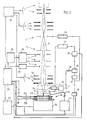
- the exemplary embodiment of an arrangement for testing and repairing an integrated circuit shown in FIG. 1 contains an ion source 1, a condenser lens 2, a blanking system 3, an aperture stop 4, a deflection device 5, a stigmator 6 and an objective lens 7.
- the objective lens 7 contains three Arranged one behind the other in the beam direction, rotationally symmetrical electrodes 7a, 7b, 7c, the axis 8 of the ion beam coinciding with the axis of the objective lens 7.
- a secondary electron spectrometer is also integrated, which essentially contains an extraction electrode 9, a filter electrode 10, a secondary electron detector 11 and a control circuit to be explained in more detail.
- the secondary electron detector 11 essentially consists of a scintillator 12, which is formed by the inner region of the central electrode 7b of the objective lens 7, a mirror 13 (or other optics) and a multiplier 14. Instead, the scintillator 12 can also be used an optical fiber can be connected to the multiplier 14.
- the device for applying an input signal to an integrated circuit 23 is formed by an LSI tester 22, which is connected to the integrated circuit 23 via a test head 15.
- the control circuit which connects the scintillator 12 to the filter electrode 10, contains the LSI tester 22 with test head 15, a phase controller 16, a delay device 17, a gate controller 18, a preamplifier 19, a signal processing circuit 20 and an amplifier 21, the output of which is connected to the filter electrode 10.
- the output of the phase control 16 connected to the delay device 17 is also connected to the blanking system 3 via a pulse generator 22.
- a data processing system 25 controls the LSI tester 22 and the phase controller 16. A corresponding return signal is led from the signal processing circuit 20 to the data processing system 25.
- the integrated circuit 23 to be examined is located on a table 26 which can be displaced in any direction perpendicular to the axis of the objective lens 7.
- the shift is done by two motors 27a, 27b controlled by the data processing system 25 via a control unit 28.
- a driver 29 is provided for actuating the deflection device 5 and is driven by the data processing system 25 via a control 30.
- the stigmator 6 is also connected to the data processing system 25 via a controller 31.
- Another controller 32 connected to the data processing system 25 controls the ion source 1, the condenser lens 2 and the objective lens 7.
- a separation device 33 is provided with a nozzle 34, which is also controlled via the data processing system 25.
- the general principle of the control loop is to regulate the secondary electron signal to a constant current and at the same time to generate the phase control for the blanking system 3 of the ion beam.
- the secondary electrons 35 triggered by the ion beam when it hits the sample 23 must first pass through the filter electrode 10 after passing through the extraction electrode 9. Since the filter electrode is at a certain negative potential (which - as will be explained - is controlled by the control loop), only the secondary electrons which have a sufficiently high energy are let through through the filter electrode 10.
- the potential at the examined measuring point of the integrated circuit 23 changes, the energy distribution of the secondary electrons shifts and accordingly more or fewer electrons come to the scintillator 12 of the secondary electron detector 11. Now the potential of the filter electrode 10 is readjusted so that the secondary electron current remains constant . The potential of the filter electrode 10 is thus changed depending on the potential to be measured on the integrated circuit 23. The changing potential of the filter electrode 10 thus represents a measure of the potential of the integrated circuit 23 to be measured.
- the outer control circuit works as follows:
- the secondary electron detector 11 converts the secondary electrons generated by the ion beam at the measuring point - provided they pass through the filter electrode 10 - into an electrical actual signal which is scanned by the gate control 18 after amplification in the preamplifier 19 .
- This scanning is controlled by the LSI tester 22, which at the same time also drives the integrated circuit 23 to be examined via the test head 15.
- the phase controller 16 enables the sampling time to be set.
- the blanking system 3 of the ion beam is controlled from the output of the phase control 16 via the pulse generator 24.
- the delay device 17 is provided.
- the device for comparing the converted actual signal with the desired signal is formed by the signal processing circuit 20.
- the output signal of the preamplifier 19 sampled via the gate control 18 can be averaged in order to improve the signal-to-noise ratio.
- a comparator is used to carry out a comparison with the target signal, which corresponds to the desired constant secondary electron current.
- the output signal reaches the filter electrode 10 via the amplifier 21 and, in the manner already explained, keeps the secondary electron current constant by changing the negative potential of the filter electrode 10, even if the potential to be measured changes at the measuring point of the integrated circuit 23 under investigation.
- a pulsed ion source can of course also be used within the scope of the invention.
- the ion beam can be adjusted to any measuring point of the integrated circuit 23 by moving the table 26 by means of the motors 27a, 27b via the control unit 28.
- the relative movement of the ion beam and the integrated circuit 23 can also be solved within the scope of the invention by, for example, shifting the axis 8 of the ion beam and thus the entire apparatus perpendicular to the integrated circuit 23.
- An input signal is applied to the integrated circuit 23 by the LSI tester 22 via the test head 15, and the resulting output signal is in turn passed on to the LSI tester 22 via the test head 15. In this way, the information is obtained as to whether there is an error in the circuit. If there is an error, 22 different test programs are generated by the LSI tester in order to limit the error.
- Measuring points are defined by means of a CAD system and the electrical description of the integrated circuit 23. The individual measuring points are approached by the ion beam in order to carry out potential measurements there in the manner described above.
- the data processing system 25 receives from the signal processing circuit 20 at each measuring point the information as to whether there is a deviation of the actual signal from the target signal. These measurements are carried out repeatedly at various measuring points until the fault is precisely localized. The choice of the individual measuring points expediently depends on the results of the previous measurements. This can be done either automatically by the data processing system 25 or by the operator.
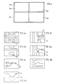
- FIGS. 4a to 4h show possible menus which can be combined in any way on the screen 36.
- FIG. 4 a shows a so-called SEM image of a section of the integrated circuit 23, which was created by scanning the integrated circuit with the ion beam.
- the reference point 37 denotes the measuring point to be examined.
- 4b shows the corresponding CAD layout over the same section of the integrated circuit 23, the position 38 corresponding to the measuring point 37 being shown from the layout.
- 4c illustrates a CAD block diagram, the measuring point 37 or the position 38 being designated by the corresponding position 39 in the block diagram.
- the waveform 40 in FIG. 4d corresponds, for example, to the waveform signal measured at the measuring point 37.
- the waveform 40 was created by simulation so that the operator can determine on the screen whether there are deviations between the measured and simulated waveform.
- the arrangement for testing and repairing an integrated circuit can also be used to carry out the repair immediately, without the integrated circuit 23 having to be implemented.
- the device for repairing an integrated circuit provided in this arrangement also uses an ion beam.
- the ion beam used for the repair also forms the ion beam used for the test process. This beam is generated in a single beam generating device, namely the ion source 1.
- conductor tracks can be cut with the ion beam, and on the other hand, conductive material can be applied to the integrated circuit by a separating device, so that new line connections are created.
- FIG. 4f A CAD layout is shown in FIG. 4f, the locations of the deposition 42 and the separation 43 being indicated.
- FIG. 4g the conductor track 44 and the cut 45 can be observed in a CAD layout.
- the separation process takes place by controlling the separation device 33 via the data processing system 25, the outlet opening of the nozzle 34 being brought into the correct position by moving the table 26.
- 4h shows a control menu in which the waveform signals generated by simulation and / or measurements can be compiled.
- the data processing system 25 has all circuit data of the integrated circuit 23, such as block diagrams, layout and mask data.
- the new integrated circuit created by a repair can in turn be stored in the data processing system and new simulations can be carried out for this circuit.
- the Time for a circuit development can be significantly reduced in this way.
- the arrangement for testing and repairing can therefore not only be used for finished integrated circuits - which are only to be checked again - but can also be used for the circuit construction in the development phase.
- the scintillator 12 is formed by the central electrode 7b of the objective lens 7.
- the scintillator 12 ' is arranged outside the objective lens 7.
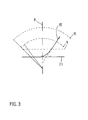
- the secondary electron spectrometer contains a pressure electrode 46 and a deflection electrode 47.
- the pressure electrode 46 and the deflection electrode 47 ensure that the secondary electrons generated after passing through the filter electrode 10 reach the scintillator 12 'arranged on the side next to the secondary electron spectrometer. Otherwise, the structure and mode of operation are analogous to the exemplary embodiment according to FIG. 1.
- the extraction electrode 9 and the filter electrode 10 are shown in FIG. 2 as planar networks, but can advantageously also be designed as spherical networks, as shown in FIG.
Landscapes
- Engineering & Computer Science (AREA)
- Power Engineering (AREA)
- General Physics & Mathematics (AREA)
- Computer Hardware Design (AREA)
- Microelectronics & Electronic Packaging (AREA)
- Physics & Mathematics (AREA)
- Condensed Matter Physics & Semiconductors (AREA)
- General Engineering & Computer Science (AREA)
- Manufacturing & Machinery (AREA)
- Testing Or Measuring Of Semiconductors Or The Like (AREA)
- Tests Of Electronic Circuits (AREA)
- Testing Of Individual Semiconductor Devices (AREA)
- Design And Manufacture Of Integrated Circuits (AREA)
Abstract
Description
Die Erfindung betrifft ein Verfahren entsprechend dem Oberbegriff des Anspruches 1 sowie eine Anordnung entsprechend dem Gattungsbegriff des Anspruches 4 zum Testen und Reparieren einer integrierten Schaltung.The invention relates to a method according to the preamble of
Es ist bekannt, zum Testen von integrierten Schaltungen ein Elektronenstrahlgerät zu verwenden. Dabei wird die mit einem Eingangssignal beaufschlagte integrierte Schaltung mit einem Elektronenstrahl abgetastet. Die an einer bestimmten Meßstelle erzeugten Sekundärelektronen werden in ein entsprechendes elektrisches Ist-Signal umgewandelt und mit dem durch das Eingangssignal bestimmten Soll-Signal verglichen. Die Reparatur einer als fehlerhaft erkannten integrierten Schaltung erfolgt dann in einem lonenstrahlgerät.It is known to use an electron beam device to test integrated circuits. The integrated circuit loaded with an input signal is scanned with an electron beam. The secondary electrons generated at a certain measuring point are converted into a corresponding actual electrical signal and compared with the desired signal determined by the input signal. The repair of an integrated circuit identified as defective is then carried out in an ion beam device.
Das Umsetzen der integrierten Schaltung aus dem Elektronenstrahlgerät in das lonenstrahlgerät hat jedoch zur Folge, daß die fehlerhafte Stelle der integrierten Schaltung erneut aufgesucht werden muß, bevor die eigentliche Reparatur mit dem lonenstrahl erfolgen kann. Die anschließende Überprüfung der erfolgten Reparatur muß wieder in einem Elektronenstrahlgerät durchgeführt werden.However, converting the integrated circuit from the electron beam device into the ion beam device means that the faulty location of the integrated circuit must be sought again before the actual repair can be carried out with the ion beam. The subsequent check of the repair must be carried out again in an electron beam device.
Neben dem großen Zeitaufwand sind für ein derartiges Test- und Reparaturverfahren viele und teure Geräte erforderlich.In addition to the large amount of time required for such a test and repair procedure, many and expensive devices are required.
Der Erfindung liegt daher die Aufgabe zugrunde, das Verfahren entsprechend dem Oberbegriff des Anspruches 1 sowie die Anordnung entsprechend dem Gattungsbegriff des Anspruches 4 derart weiterzubilden, daß der mit dem Testen und Reparieren einer integrierten Schaltung verbundene Zeit- und Kostenaufwand im Vergleich zum Stand der Technik wesentlich gesenkt wird.The invention is therefore based on the object of developing the method according to the preamble of
Diese Aufgabe wird erfindungsgemäß dadurch gelöst, daß der für die Reparatur verwendete lonenstrahl zugleich den für den Testvorgang benutzten Korpuskularstrahl bildet und zur Erzeugung dieses Strahles eine einzige Strahlerzeugungseinrichtung vorgesehen ist.This object is achieved in that the ion beam used for the repair also forms the corpuscular beam used for the test process and a single beam generating device is provided for generating this beam.
Dadurch entfällt das zeitaufwendige Umsetzen der integrierten Schaltung zwischen einer Vorrichtung zum Testen und einer Vorrichtung zum Reparieren. Nachdem der erzeugte lonenstrahl sowohl zum Testen als auch zum Reparieren der integrierten Schaltung verwendet wird, reicht eine einzige Strahlerzeugungseinrichtung aus, wodurch sich der Kostenaufwand erheblich reduziert.This eliminates the time-consuming implementation of the integrated circuit between a device for testing and a device for repairing. Since the ion beam generated is used both for testing and for repairing the integrated circuit, a single beam generating device is sufficient, which considerably reduces the cost.
Weitere Merkmale der Erfindung sind Gegenstand der Unteransprüche und werden in der Zeichnung und der folgenden Beschreibung näher erläutert.Further features of the invention are the subject of the dependent claims and are explained in more detail in the drawing and the following description.
In der Zeichnung zeigen
- Fig.1 eine schematische Darstellung eines ersten Ausführungsbeispieles,
- Fig.2 eine schematische Darstellung eines zweiten Ausführungsbeispieles,
- Fig.3 eine schematische Darstellung eines Ausführungsbeispieles eines Sekundärelektronenspektrometers,
- Fig.4, 4a bis 4h Menüdarstellungen auf einem Bildschirm.
- 1 shows a schematic illustration of a first exemplary embodiment,
- 2 shows a schematic illustration of a second exemplary embodiment,
- 3 shows a schematic illustration of an exemplary embodiment of a secondary electron spectrometer,
- Fig. 4, 4a to 4h menu displays on a screen.
Das in Fig.1 dargestellte Ausführungsbeispiel einer Anordnung zum Testen und Reparieren einer integrierten Schaltung enthält eine lonenquelle 1, eine Kondensorlinse 2, ein Austastsystem 3, eine Aperturblende 4, eine Ablenkeinrichtung 5, einen Stigmator 6 sowie eine Objektivlinse 7. Die Objektivlinse 7 enthält drei in Strahlrichtung hintereinander angeordnete, rotationssymmetrische Elektroden 7a, 7b, 7c, wobei die Achse 8 des lonenstrahls mit der Achse der Objektivlinse 7 zusammenfällt.The exemplary embodiment of an arrangement for testing and repairing an integrated circuit shown in FIG. 1 contains an
In diese Anordnung ist ferner ein Sekundärelektronenspektrometer integriert, das im wesentlichen eine Extraktionselektrode 9, eine Filterelektrode 10, einen Sekundärelektronendetektor 11 und einen noch näher zu erläuternden Regelkreis enthält.In this arrangement, a secondary electron spectrometer is also integrated, which essentially contains an
Der Sekundärelektronendetektor 11 besteht im wesentlichen aus einem Szintillator 12, der durch den inneren Bereich der mittleren Elektrode 7b der Objektivlinse 7 gebildet wird, ferner aus einem Spiegel 13 (oder einer sonstigen Optik) sowie einem Multiplier 14. Statt dessen kann der Szintillator 12 auch über einen Lichtleiter mit dem Multiplier 14 verbunden sein.The
Die Einrichtung zur Beaufschlagung einer integrierten Schaltung 23 mit einem Eingangssignal wird durch einen LSI-Tester 22 gebildet, der über einen Testkopf 15 mit der integrierten Schaltung 23 verbunden ist.The device for applying an input signal to an
Der Regelkreis, der den Szintillator 12 mit der Filterelektrode 10 verbindet, enthält den LSI-Tester 22 mit Testkopf 15, eine Phasensteuerung 16, eine Verzögerungseinrichtung 17, eine Torsteuerung 18, einen Vorverstärker 19, eine signalverarbeitende Schaltung 20 sowie einen Verstärker 21, dessen Ausgang an die Filterelektrode 10 angeschlossen ist.The control circuit, which connects the
Der mit der Verzögerungseinrichtung 17 verbundene Ausgang der Phasensteuerung 16 ist weiterhin über einen Pulsgenerator 22 an das Austastsystem 3 angeschlossen.The output of the
Eine datenverarbeitende Anlage 25 steuert den LSI-Tester 22 sowie die Phasensteuerung 16 an. Ein entsprechendes Rücksignal wird von der signalverarbeitenden Schaltung 20 zur datenverarbeitenden Anlage 25 geführt.A
Die zu untersuchende integrierte Schaltung 23 befindet sich auf einem Tisch 26, der beliebig in senkrechter Richtung zur Achse der Objektivlinse 7 verschiebbar ist. Die Verschiebung erfolgt durch zwei von der datenverarbeitenden Anlage 25 über eine Steuereinheit 28 gesteuerte Motoren 27a, 27b.The integrated
Zur Betätigung der Ablenkeinrichtung 5 ist ein Treiber 29 vorgesehen, der über eine Steuerung 30 von der datenverarbeitenden Anlage 25 angetrieben wird. Der Stigmator 6 ist über eine Steuerung 31 ebenfalls mit der datenverarbeitenden Anlage 25 verbunden. Eine weitere mit der datenverarbeitenden Anlage 25 in Verbindung stehende Steuerung 32 steuert die lonenquelle 1, die Kondensorlinse 2 und die Objektivlinse 7.A
Zur Abscheidung von leitendem Material auf der integrierten Schaltung 23 ist eine Abscheidevorrichtung 33 mit einer Düse 34 vorgesehen, die auch über die datenverarbeitende Anlage 25 angesteuert wird.For the separation of conductive material on the
Mit der Anordnung gemäß Fig.1 ist einerseits eine Vorrichtung zum Testen und andererseits eine Vorrichtung zum Reparieren einer integrierten Schaltung verwirklicht. Zunächst wird die Funktionsweise während des Testvorganges näher beschrieben:
- Der auf die
integrierte Schaltung 23 fokussierte lonenstrahl löst, in Abhängigkeit vom Potential an dieser Stelle, eine entsprechende Anzahl anSekundärelektronen 35 aus.
- The ion beam focused on the
integrated circuit 23 triggers a corresponding number ofsecondary electrons 35 depending on the potential at this point.
Das allgemeine Prinzip des Regelkreises besteht darin, das Sekundärelektronensignal auf konstanten Strom zu regeln und gleichzeitig die Phasensteuerung für das Austastsystem 3 des lonenstrahls zu erzeugen.The general principle of the control loop is to regulate the secondary electron signal to a constant current and at the same time to generate the phase control for the
Die vom lonenstrahl beim Auftreffen auf die Probe 23 ausgelösten Sekundärelektronen 35 müssen nach Passieren der Extraktionselektrode 9 zunächst die Filterelektrode 10 passieren. Da die Filterelektrode auf einem bestimmten negativen Potential liegt (das - wie noch erläutert wird - vom Regelkreis gesteuert wird), werden nur die Sekundärelektronen durch die Filterelektrode 10 durchgelassen, die eine genügend hohe Energie besitzen.The
Wenn sich das Potential an der untersuchten Meßstelle der integrierten Schaltung 23 ändert, verschiebt sich die Energieverteilung der Sekundärelektronen und es kommen entsprechend mehr oder weniger Elektronen zum Szintillator 12 des Sekundärelektronendetektors 11. Nunmehr wird das Potential der Filterelektrode 10 so nachgeregelt, daß der Sekundärelektronenstrom konstant bleibt. Das Potential der Filterelektrode 10 wird somit in Abhängigkeit von dem zu messenden Potential auf der integrierten Schaltung 23 geändert. Damit stellt das sich ändernde Potential der Filterelektrode 10 ein Maß für das zu messende Potential der integrierten Schaltung 23 dar.If the potential at the examined measuring point of the
Im einzelnen arbeitet der äußere Regelkreis wie folgt: Der Sekundärelektronendetektor 11 wandelt die durch den lonenstrahl an der Meßstelle erzeugten Sekundärelektronen - sofern sie die Filterelektrode 10 passieren - in ein elektrisches Ist-Signal um, das nach Verstärkung im Vorverstärker 19 durch die Torsteuerung 18 abgetastet wird. Diese Abtastung wird durch den LSI-Tester 22 gesteuert, der zugleich auch über den Testkopf 15 die zu untersuchende integrierte Schaltung 23 treibt. Die Phasensteuerung 16 ermöglicht hierbei die Einstellung des Abtastzeitpunktes.In detail, the outer control circuit works as follows: The
Vom Ausgang der Phasensteuerung 16 wird über den Pulsgenerator 24 das Austastsystem 3 des lonenstrahls gesteuert. Um die Laufzeit des lonenstrahls vom Austastsystem 3 bis zur integrierten Schaltung 23 zu berücksichtigen, ist die Verzögerungseinrichtung 17 vorgesehen.The
Die Einrichtung zum Vergleichen des umgewandelten Ist-Signals mit dem Soll-Signal wird durch die signalverarbeitende Schaltung 20 gebildet. In der signalverarbeitenden Schaltung 20 kann das über die Torsteuerung 18 abgetastete Ausgangssignal des Vorverstärkers 19 gemittelt werden, um das Signal-Rausch-Verhältnis zu verbessern. Mittels eines Komparators wird ein Vergleich mit dem Soll-Signal durchgeführt, der dem gewünschten konstanten Sekundärelektronenstrom entspricht. Das Ausgangssignal gelangt über den Verstärker 21 zur Filterelektrode 10 und hält in der bereits erläuterten Weise durch Änderung des negativen Potentials der Filterelektrode 10 den Sekundärelektronenstrom konstant, auch wenn sich das zu messende Potential auf der untersuchten Meßstelle der integrierten Schaltung 23 ändert.The device for comparing the converted actual signal with the desired signal is formed by the
Statt eines Austastsystems 3 zum Austasten (Blanken) des lonenstrahls kann im Rahmen der Erfindung selbstverständlich auch eine gepulste lonenquelle Verwendung finden.Instead of a
Der lonenstrahl kann durch Verschiebung des Tisches 26 mittels der Motoren 27a, 27b über die Steuereinheit 28 auf jede beliebige Meßstelle der integrierten Schaltung 23 eingestellt werden. Ferner besteht die Möglichkeit, den lonenstrahl über die Steuerung 30 und den Treiber 29 der Ablenkeinrichtung 5 auf der integrierten Schaltung zu verschieben. Die Relativbewegung von lonenstrahl und integrierter Schaltung 23 kann im Rahmen der Erfindung auch dadurch gelöst werden, daß beispielsweise die Achse 8 des lonenstrahls und damit die gesamte Apparatur senkrecht zur integrierten Schaltung 23 verschoben wird.The ion beam can be adjusted to any measuring point of the integrated
Über den Testkopf 15 wird die integrierte Schaltung 23 vom LSI-Tester 22 mit einem Eingangssignal beaufschlagt, und das entstehende Ausgangssignal wird wiederum über den Testkopf 15 zum LSI-Tester 22 weitergeleitet. Auf diese Weise ergibt sich die Information, ob ein Fehler in der Schaltung vorliegt. Liegt ein Fehler vor, werden vom LSI-Tester 22 verschiedene Testprogramme erzeugt, um den Fehler einzugrenzen.An input signal is applied to the
Nach dieser groben Fehlerlokalisierung muß gezielt im Schaltungsinneren gemessen werden. Mittels eines CAD-Systems und der elektrischen Beschreibung der integrierten Schaltung 23 werden Meßstellen festgelegt. Die einzelnen Meßstellen werden vom lonenstrahl angefahren, um dort Potentialmessungen in der oben beschriebenen Art und Weise durchzuführen.After this rough error localization be measured specifically inside the circuit. Measuring points are defined by means of a CAD system and the electrical description of the
Die datenverarbeitende Anlage 25 erhält von der signalverarbeitenden Schaltung 20 an jeder Meßstelle die Information, ob eine Abweichung des Ist-Signales gegenüber dem Soll-Signal vorliegt. Diese Messungen werden an verschiedenen Meßstellen wiederholt durchgeführt, bis der Fehler exakt lokalisiert ist. Dabei richtet sich zweckmäßigerweise die Wahl der einzelnen Meßstellen nach den Ergebnissen der vorangegangenen Messungen. Dies kann entweder automatisch von der datenverarbeitenden Anlage 25 oder vom Operator erfolgen.The
Auf einem in Fig.4 dargestellten Bildschirm 36 der datenverarbeitenden Anlage 25 können von der zu untersuchenden integrierten Schaltung 23 verschiedene Darstellungen angezeigt werden. Die Figuren 4a bis 4h zeigen mögliche Menüs, die auf dem Bildschirm 36 in beliebiger Weise kombiniert werden können.Various representations of the
Fig.4a zeigt ein sogenanntes SEM-Bild eines Ausschnittes aus der integrierten Schaltung 23, das durch Rasterung der integrierten Schaltung mit dem lonenstrahl entstanden ist. Mit dem Bezugszeichen 37 ist die gerade zu untersuchende Meßstelle bezeichnet.4 a shows a so-called SEM image of a section of the
Fig.4b zeigt über den gleichen Ausschnitt der integrierten Schaltung 23 das entsprechende CAD-Layout, wobei die der Meßstelle 37 entsprechende Position 38 aus dem Layout gezeigt ist.4b shows the corresponding CAD layout over the same section of the
Fig.4c veranschaulicht ein CAD-Blockschaltbild, wobei die Meßstelle 37 bzw. die Position 38 mit der entsprechenden Position 39 im Blockschaltbild bezeichnet ist.4c illustrates a CAD block diagram, the measuring
Der Wellenform 40 in Fig.4d entspricht die Wellenform 41 beispielsweise dem an der Meßstelle 37 gemessenen Wellenformsignal. Die Wellenform 40 ist durch Simulation entstanden, so daß der Operator am Bildschirm feststellen kann, ob zwischen gemessener und simulierter Wellenform Abweichungen bestehen.The
Ist der Fehler eindeutig lokalisiert, läßt sich mit Hilfe der Anordnung zum Testen und Reparieren einer integrierten Schaltung unmittelbar auch die Reparatur durchführen, ohne daß die integrierte Schaltung 23 umgesetzt werden muß. Die in dieser Anordnung vorgesehene Vorrichtung zur Reparatur einer integrierten Schaltung verwendet ebenfalls einen lonenstrahl. Dabei bildet der für die Reparatur verwendete lonenstrahl zugleich den für den Testvorgang benutzten lonenstrahl. Die Erzeugung dieses Strahles erfolgt in einer einzigen Strahlerzeugungseinrichtung, nämlich der lonenquelle 1.If the fault is clearly localized, the arrangement for testing and repairing an integrated circuit can also be used to carry out the repair immediately, without the
Zur Reparatur einer integrierten Schaltung stehen im wesentlichen zwei Möglichkeiten zur Verfügung. Einerseits können mit dem lonenstrahl Leiterbahnen aufgetrennt werden, und andererseits kann durch eine Abscheideeinrichtung leitendes Material auf die integrierte Schaltung aufgebracht werden, so daß neue Leitungsverbindungen entstehen.There are essentially two options for repairing an integrated circuit. On the one hand, conductor tracks can be cut with the ion beam, and on the other hand, conductive material can be applied to the integrated circuit by a separating device, so that new line connections are created.
Welche dieser beiden Möglichkeiten zur Behebung einer Fehlerstelle angewandt wird, hängt vom Einzelfall ab. In Fig.4f ist ein CAD-Layout dargestellt, wobei die Stellen der Abscheidung 42 und der Auftrennung 43 angedeutet sind. In Fig.4g kann wiederum in einem CAD-Layout die durch Abscheidung neu entstandene Leiterbahn 44 und die aufgeschnittene Stelle 45 beobachtet werden.Which of these two options is used to correct a fault depends on the individual case. A CAD layout is shown in FIG. 4f, the locations of the
Der Abscheidevorgang erfolgt durch Steuerung der Abscheideeinrichtung 33 über die datenverarbeitende Anlage 25, wobei die Austrittsöffnung der Düse 34 durch Verfahren des Tisches 26 in die richtige Position gebracht wird.The separation process takes place by controlling the separation device 33 via the
Fig.4h zeigt ein Kontrollmenü, in dem die durch Simulation und/oder Messungen entstandenen Wellenformsignale zusammengestellt werden können.4h shows a control menu in which the waveform signals generated by simulation and / or measurements can be compiled.
Die Menüs gemäß den Fig.4a bis 4h sind nur als beispielhafte Zusammenstellungen anzusehen und können für spezielle Anwendungen entsprechend abgeändert bzw. ergänzt werden. Die Zahl der auf dem Bildschirm 36 gleichzeitig angezeigten Menüs ist keineswegs auf die in Fig.4 dargestellte Anzahl von vier Menüs 36a bis 36d beschränkt. Vielmehr können je nach Anwendung nur ein Menü oder auch beliebig viele Menüs kombiniert werden. Die Verwirklichung der Vorrichtung zum Testen und der Vorrichtung zum Reparieren in einer Anordnung, wobei nur eine einzige Strahlerzeugungseinrichtung vorgesehen ist, erweist sich besonders in folgenden Punkten als hilfreich:
- a) Der LSI-
Tester 22 kann die integrierte Schaltung 23 mit einem Eingangssignal beaufschlagen, so daß unmittelbar bestätigt werden kann, ob der angefahrene Meßpunkt genau der lokalisierten Fehlerstelle entspricht. - b) Der LSI-
Tester 22 kann schnell und leicht prüfen, ob beispielsweise eine Leiterbahn wirklich aufgetrennt worden ist, oder ob die durch abgeschiedenes Material neu entstandene Leiterbahn guten und gezielten Kontakt mit anderen Leiterbahnen hat.
- a) The
LSI tester 22 can apply an input signal to theintegrated circuit 23 so that it can be immediately confirmed whether the approached measuring point corresponds exactly to the localized fault location. - b) The
LSI tester 22 can quickly and easily check whether, for example, a conductor track has really been cut, or whether the conductor track newly formed by the separated material has good and targeted contact with other conductor tracks.
Die datenverarbeitende Anlage 25 verfügt über sämtliche Schaltungsdaten der integrierten Schaltung 23, wie beispielsweise Blockschaltbilder, Layout- und Maskendaten. Die neue, durch eine Reparatur entstandene integrierte Schaltung kann wiederum in der datenverarbeitenden Anlage abgespeichert werden, und es können neue Simulationen für diese Schaltung vorgenommen werden. Die Zeit für eine Schaltungsentwicklung läßt sich auf diese Weise deutlich reduzieren.The
Die Anordnung zum Testen und Reparieren ist demnach nicht nur für fertige integrierte Schaltungen - die lediglich noch einmal überprüft werden sollen - verwendbar, sondern auch für den Schaltungsaufbau in der Entwicklungsphase einsetzbar. In diesem Zusammenhang ist es auch denkbar, im Rahmen der Erfindung eine weitere Einrichtung vorzusehen, mit deren Hilfe Bauteile, wie beispielsweise Widerstände oder Transistoren auf die integrierte Schaltung aufgebracht werden können.The arrangement for testing and repairing can therefore not only be used for finished integrated circuits - which are only to be checked again - but can also be used for the circuit construction in the development phase. In this context, it is also conceivable to provide a further device within the scope of the invention, by means of which components, such as, for example, resistors or transistors, can be applied to the integrated circuit.
Im ersten Ausführungsbeispiel gemäß Fig.4 wird der Szintillator 12 durch die mittlere Elektrode 7b der Objektivlinse 7 gebildet. Im Ausführungsbeispiel gemäß Fig.2 ist der Szintillator 12' außerhalb der Objektivlinse 7 angeordnet.In the first exemplary embodiment according to FIG. 4, the
Das Sekundärelektronenspektrometer enthält neben der Extraktionselektrode 9 und der Filterelektrode 10 eine Druckelektrode 46 sowie eine Umlenkelektrode 47. Die Druckelektrode 46 und die Umlenkelektrode 47 gewährleisten dabei, daß die erzeugten Sekundärelektronen nach Passieren der Filterelektrode 10 den seitlich neben dem Sekundärelektronenspektrometer angeordneten Szintillator 12' erreichen. Im übrigen ist der Aufbau und die Funktionsweise analog zum Ausführungsbeispiel gemäß Fig.1. Die Extraktionselektrode 9 und die Filterelektrode 10 sind in Fig.2 als planare Netze dargestellt, können jedoch vorteilhafterweise auch als Kugelnetze ausgebildet sein, wie dies in Fig.3 dargestellt ist.In addition to the
Claims (10)
dadurch gekennzeichnet, daß
characterized in that
dadurch gekennzeichnet, daß
characterized in that
Applications Claiming Priority (2)
| Application Number | Priority Date | Filing Date | Title |
|---|---|---|---|
| DE4027062 | 1990-08-27 | ||
| DE4027062A DE4027062A1 (en) | 1990-08-27 | 1990-08-27 | METHOD AND ARRANGEMENT FOR TESTING AND REPAIRING AN INTEGRATED CIRCUIT |
Publications (3)
| Publication Number | Publication Date |
|---|---|
| EP0472938A2 true EP0472938A2 (en) | 1992-03-04 |
| EP0472938A3 EP0472938A3 (en) | 1992-06-17 |
| EP0472938B1 EP0472938B1 (en) | 1996-06-19 |
Family
ID=6413010
Family Applications (1)
| Application Number | Title | Priority Date | Filing Date |
|---|---|---|---|
| EP91112862A Expired - Lifetime EP0472938B1 (en) | 1990-08-27 | 1991-07-31 | Device for testing and repairing an integrated circuit |
Country Status (4)
| Country | Link |
|---|---|
| US (1) | US5214284A (en) |
| EP (1) | EP0472938B1 (en) |
| JP (1) | JP3330382B2 (en) |
| DE (2) | DE4027062A1 (en) |
Cited By (2)
| Publication number | Priority date | Publication date | Assignee | Title |
|---|---|---|---|---|
| EP1777729A1 (en) * | 2004-08-11 | 2007-04-25 | Hitachi High-Technologies Corporation | Scanning type electron microscope |
| DE102010064569B3 (en) | 2010-07-06 | 2022-10-13 | Carl Zeiss Multisem Gmbh | Particle beam system and method for operating a particle beam system |
Families Citing this family (7)
| Publication number | Priority date | Publication date | Assignee | Title |
|---|---|---|---|---|
| DE4216730C2 (en) * | 1992-05-20 | 2003-07-24 | Advantest Corp | Scanning electron beam device |
| JP3564958B2 (en) * | 1997-08-07 | 2004-09-15 | 株式会社日立製作所 | Inspection method and inspection apparatus using electron beam |
| US6234030B1 (en) | 1998-08-28 | 2001-05-22 | Rosewood Equipment Company | Multiphase metering method for multiphase flow |
| US6164308A (en) | 1998-08-28 | 2000-12-26 | Butler; Bryan V. | System and method for handling multiphase flow |
| FR2792455B1 (en) * | 1999-04-16 | 2003-02-28 | Centre Nat Etd Spatiales | METHOD AND INSTALLATION FOR CORRECTING AN INTEGRATED CIRCUIT BY AN ION BEAM CONTROLLED BY THE PROFILE OF THE VARIATIONS IN THE RATE OF DETECTED SECONDARY PARTICLES |
| EP1482532A1 (en) * | 2003-05-26 | 2004-12-01 | ICT Integrated Circuit Testing Gesellschaft für Halbleiterprüftechnik mbH | Gradient field deflector |
| CN113394534B (en) * | 2021-08-16 | 2021-11-26 | 南京华脉科技股份有限公司 | Ware is divided to combination formula merit convenient to overhaul |
Citations (5)
| Publication number | Priority date | Publication date | Assignee | Title |
|---|---|---|---|---|
| JPS6028151A (en) * | 1983-07-27 | 1985-02-13 | Mitsubishi Electric Corp | Scanning type strobo ion microscope |
| JPS6410561A (en) * | 1987-07-02 | 1989-01-13 | Akashi Biimu Technol Kk | Electrostatic lens with secondary electron detector function |
| JPH01181528A (en) * | 1988-01-11 | 1989-07-19 | Seiko Instr & Electron Ltd | Ion beam processing device |
| US4983830A (en) * | 1989-06-29 | 1991-01-08 | Seiko Instruments Inc. | Focused ion beam apparatus having charged particle energy filter |
| DE4000579A1 (en) * | 1990-01-10 | 1991-07-11 | Integrated Circuit Testing | ION RAY DEVICE AND METHOD FOR CARRYING OUT POTENTIAL MEASURES BY MEANS OF AN ION RAY |
Family Cites Families (9)
| Publication number | Priority date | Publication date | Assignee | Title |
|---|---|---|---|---|
| SE452526B (en) * | 1984-05-09 | 1987-11-30 | Stiftelsen Inst Mikrovags | PROCEDURE TO INSPECT INTEGRATED CIRCUITS OR OTHER OBJECTS |
| DE3576213D1 (en) * | 1984-09-18 | 1990-04-05 | Integrated Circuit Testing | COUNTERFIELD SPECTROMETER FOR ELECTRON BEAM MEASURING TECHNOLOGY. |
| DE3437550A1 (en) * | 1984-10-12 | 1986-04-24 | Siemens AG, 1000 Berlin und 8000 München | METHOD FOR FAULT ANALYSIS ON INTEGRATED CIRCUITS |
| JPS6298544A (en) * | 1985-10-25 | 1987-05-08 | Hitachi Ltd | Charged particle ray device |
| DE3638682A1 (en) * | 1986-11-13 | 1988-05-19 | Siemens Ag | SPECTROMETER LENS FOR CARPUSULAR BEAM MEASUREMENT TECHNOLOGY |
| US4853628A (en) * | 1987-09-10 | 1989-08-01 | Gazelle Microcircuits, Inc. | Apparatus for measuring circuit parameters of a packaged semiconductor device |
| US4908226A (en) * | 1988-05-23 | 1990-03-13 | Hughes Aircraft Company | Selective area nucleation and growth method for metal chemical vapor deposition using focused ion beams |
| US5083033A (en) * | 1989-03-31 | 1992-01-21 | Kabushiki Kaisha Toshiba | Method of depositing an insulating film and a focusing ion beam apparatus |
| DE3938660A1 (en) * | 1989-11-21 | 1991-05-23 | Integrated Circuit Testing | BODY RADIATOR |
-
1990
- 1990-08-27 DE DE4027062A patent/DE4027062A1/en not_active Withdrawn
-
1991
- 1991-07-31 EP EP91112862A patent/EP0472938B1/en not_active Expired - Lifetime
- 1991-07-31 DE DE59107944T patent/DE59107944D1/en not_active Expired - Fee Related
- 1991-08-14 US US07/744,933 patent/US5214284A/en not_active Expired - Lifetime
- 1991-08-27 JP JP21561691A patent/JP3330382B2/en not_active Expired - Fee Related
Patent Citations (5)
| Publication number | Priority date | Publication date | Assignee | Title |
|---|---|---|---|---|
| JPS6028151A (en) * | 1983-07-27 | 1985-02-13 | Mitsubishi Electric Corp | Scanning type strobo ion microscope |
| JPS6410561A (en) * | 1987-07-02 | 1989-01-13 | Akashi Biimu Technol Kk | Electrostatic lens with secondary electron detector function |
| JPH01181528A (en) * | 1988-01-11 | 1989-07-19 | Seiko Instr & Electron Ltd | Ion beam processing device |
| US4983830A (en) * | 1989-06-29 | 1991-01-08 | Seiko Instruments Inc. | Focused ion beam apparatus having charged particle energy filter |
| DE4000579A1 (en) * | 1990-01-10 | 1991-07-11 | Integrated Circuit Testing | ION RAY DEVICE AND METHOD FOR CARRYING OUT POTENTIAL MEASURES BY MEANS OF AN ION RAY |
Non-Patent Citations (9)
| Title |
|---|
| - 240; H.FUJIOKA ET AL.: 'Recent Topics on Electron Beam Testing in Japan' * |
| INT. CONF. ON WAFER SCALE INTEGRATION 1989 Januar 1989, SAN FRANCISCO US Seiten 161 - 172; J.F.MCDONALD ET AL.: 'Application of Focused Ion Beam for Testing, Repair and Fabrication of Metal and Optical Interconnections in Wafer Scale Integration' * |
| JOURNAL OF VACUUM SCIENCE AND TECHNOLOGY: PART B. Bd. 4, Nr. 1, Januar 1986, NEW YORK US Seiten 185 - 188; D.C.SHAVER ET AL.: 'Integrated circuit diagnosis using focused ion beams' * |
| MICROELECTRONIC ENGINEERING. Bd. 12, Nr. 1/4, Mai 1990, AMSTERDAM NL Seiten 15 - 26; D.W.RANASINGHE ET AL.: 'Design Verification and Quality Control of Integrated Circuits in an Industrial Environment' * |
| MICROELECTRONIC ENGINEERING. Bd. 12, Nr. 1/4, Mai 1990, AMSTERDAM NL Seiten 237 - 240; H.FUJIOKA ET AL.: 'Recent Topics on Electron Beam Testing in Japan' * |
| PATENT ABSTRACTS OF JAPAN vol. 13, no. 184 (E-751)28. April 1989 & JP-A-1 010 561 ( AKASHI BIIMU TECHNOL ) 13. Januar 1989 * |
| PATENT ABSTRACTS OF JAPAN vol. 9, no. 147 (E-323)(1870) 21. Juni 1985 & JP-A-60 028 151 ( MITSUBISHI DENKI ) 13. Februar 1985 * |
| Patent Abstracts of Japan, Bd. 13, Nr. 468 (E834), veröffentlicht am 23.10.89. * |
| Patent Abstracts of Japan, Bd.13, Nr. 468 (E834), veröffentlicht am 23.10.89 * |
Cited By (4)
| Publication number | Priority date | Publication date | Assignee | Title |
|---|---|---|---|---|
| EP1777729A1 (en) * | 2004-08-11 | 2007-04-25 | Hitachi High-Technologies Corporation | Scanning type electron microscope |
| EP1777729A4 (en) * | 2004-08-11 | 2009-09-16 | Hitachi High Tech Corp | Scanning type electron microscope |
| US8698080B2 (en) | 2004-08-11 | 2014-04-15 | Hitachi High-Technologies Corporation | Scanning electron microscope |
| DE102010064569B3 (en) | 2010-07-06 | 2022-10-13 | Carl Zeiss Multisem Gmbh | Particle beam system and method for operating a particle beam system |
Also Published As
| Publication number | Publication date |
|---|---|
| JPH04297051A (en) | 1992-10-21 |
| JP3330382B2 (en) | 2002-09-30 |
| DE4027062A1 (en) | 1992-04-23 |
| EP0472938A3 (en) | 1992-06-17 |
| US5214284A (en) | 1993-05-25 |
| EP0472938B1 (en) | 1996-06-19 |
| DE59107944D1 (en) | 1996-07-25 |
Similar Documents
| Publication | Publication Date | Title |
|---|---|---|
| EP0014304B1 (en) | Method and apparatus for the contactless measuring of the potential on an electronic element | |
| EP0189777B1 (en) | Particle beam measuring method for the contactless testing of circuit networks | |
| DE69332995T2 (en) | Scanning electron microscope | |
| DE102018007652A1 (en) | Particle beam system and method for current regulation of individual particle beams | |
| DE3689490T2 (en) | Electron beam test probe for examining integrated circuits. | |
| DE2436160B2 (en) | Scanning electron microscope | |
| DE3605129A1 (en) | CARGO PARTICLE RADIATION DEVICE | |
| DE2441421A1 (en) | METHOD AND DEVICE FOR DIRECTING ELECTRON BEAMS | |
| DE3636316C2 (en) | ||
| EP0461442A2 (en) | Particle beam apparatus | |
| DE1943140B2 (en) | METHOD OF ANALYZING THE SURFACE POTENTIAL OF A DUTY | |
| DE3206374C2 (en) | Method and apparatus for calibrating the deflection of a beam composed of charged particles | |
| DE3031814A1 (en) | ELECTRON BEAM DEVICE | |
| DE2461202A1 (en) | METHOD AND DEVICE FOR AUTOMATIC FOCUSING OF AN ELECTRON BEAM IN A SCANNING DEVICE | |
| EP0472938B1 (en) | Device for testing and repairing an integrated circuit | |
| DE19802848B4 (en) | Method and apparatus for testing a substrate | |
| EP0048857A1 (en) | Arrangement for the stroboscopic measuring of a potential with an electron beam measuring apparatus, and method of operating such an apparatus | |
| EP0216750B1 (en) | Ion beam apparatus and process for realizing modifications, especially corrections, on substrates, using an ion beam apparatus | |
| EP0440901B1 (en) | Ion beam apparatus as well as a process to perform potential measurements by means of an ion beam | |
| DE2937136C2 (en) | ||
| DE3430984A1 (en) | METHOD AND DEVICE FOR REGISTERING PARTICLES OR QUANTS WITH THE AID OF A DETECTOR | |
| DE1564658B2 (en) | METHOD OF FOCUSING THE OBJECTIVE LENS OF A BODY OF CULAR BEAM MICROSCOPE, IN PARTICULAR AN ELECTRON MICROSCOPE | |
| DE2440120A1 (en) | DEVICE FOR REPLAYING THE ENERGY DISTRIBUTION OF A JET CONSISTING OF CHARGED PARTICLES | |
| EP0232790A1 (en) | Process and arrangement for measuring time-dependent signals with a corpuscular beam probe | |
| DE112019007662T5 (en) | Charged particle beam device and test method |
Legal Events
| Date | Code | Title | Description |
|---|---|---|---|
| PUAI | Public reference made under article 153(3) epc to a published international application that has entered the european phase |
Free format text: ORIGINAL CODE: 0009012 |
|
| AK | Designated contracting states |
Kind code of ref document: A2 Designated state(s): DE FR GB NL |
|
| PUAL | Search report despatched |
Free format text: ORIGINAL CODE: 0009013 |
|
| AK | Designated contracting states |
Kind code of ref document: A3 Designated state(s): DE FR GB NL |
|
| 17P | Request for examination filed |
Effective date: 19921006 |
|
| 17Q | First examination report despatched |
Effective date: 19940722 |
|
| RAP1 | Party data changed (applicant data changed or rights of an application transferred) |
Owner name: ICT INTEGRATED CIRCUIT TESTING GESELLSCHAFT FUER H Owner name: ADVANTEST CORPORATION |
|
| GRAH | Despatch of communication of intention to grant a patent |
Free format text: ORIGINAL CODE: EPIDOS IGRA |
|
| RAP1 | Party data changed (applicant data changed or rights of an application transferred) |
Owner name: ADVANTEST CORPORATION Owner name: ACT ADVANCED CIRCUIT TESTING GESELLSCHAFT FUER TES |
|
| GRAH | Despatch of communication of intention to grant a patent |
Free format text: ORIGINAL CODE: EPIDOS IGRA |
|
| REG | Reference to a national code |
Ref country code: GB Ref legal event code: 732E |
|
| GRAA | (expected) grant |
Free format text: ORIGINAL CODE: 0009210 |
|
| RAP1 | Party data changed (applicant data changed or rights of an application transferred) |
Owner name: ADVANTEST CORPORATION |
|
| AK | Designated contracting states |
Kind code of ref document: B1 Designated state(s): DE FR GB NL |
|
| REF | Corresponds to: |
Ref document number: 59107944 Country of ref document: DE Date of ref document: 19960725 |
|
| ET | Fr: translation filed | ||
| GBT | Gb: translation of ep patent filed (gb section 77(6)(a)/1977) |
Effective date: 19960731 |
|
| PLBE | No opposition filed within time limit |
Free format text: ORIGINAL CODE: 0009261 |
|
| STAA | Information on the status of an ep patent application or granted ep patent |
Free format text: STATUS: NO OPPOSITION FILED WITHIN TIME LIMIT |
|
| 26N | No opposition filed | ||
| REG | Reference to a national code |
Ref country code: GB Ref legal event code: IF02 |
|
| PGFP | Annual fee paid to national office [announced via postgrant information from national office to epo] |
Ref country code: DE Payment date: 20070921 Year of fee payment: 17 |
|
| PGFP | Annual fee paid to national office [announced via postgrant information from national office to epo] |
Ref country code: GB Payment date: 20070622 Year of fee payment: 17 |
|
| PGFP | Annual fee paid to national office [announced via postgrant information from national office to epo] |
Ref country code: NL Payment date: 20070613 Year of fee payment: 17 |
|
| PGFP | Annual fee paid to national office [announced via postgrant information from national office to epo] |
Ref country code: FR Payment date: 20070611 Year of fee payment: 17 |
|
| GBPC | Gb: european patent ceased through non-payment of renewal fee |
Effective date: 20080731 |
|
| NLV4 | Nl: lapsed or anulled due to non-payment of the annual fee |
Effective date: 20090201 |
|
| PG25 | Lapsed in a contracting state [announced via postgrant information from national office to epo] |
Ref country code: DE Free format text: LAPSE BECAUSE OF NON-PAYMENT OF DUE FEES Effective date: 20090203 |
|
| REG | Reference to a national code |
Ref country code: FR Ref legal event code: ST Effective date: 20090331 |
|
| PG25 | Lapsed in a contracting state [announced via postgrant information from national office to epo] |
Ref country code: NL Free format text: LAPSE BECAUSE OF NON-PAYMENT OF DUE FEES Effective date: 20090201 |
|
| PG25 | Lapsed in a contracting state [announced via postgrant information from national office to epo] |
Ref country code: GB Free format text: LAPSE BECAUSE OF NON-PAYMENT OF DUE FEES Effective date: 20080731 |
|
| PG25 | Lapsed in a contracting state [announced via postgrant information from national office to epo] |
Ref country code: FR Free format text: LAPSE BECAUSE OF NON-PAYMENT OF DUE FEES Effective date: 20080731 |