EP0472717B1 - Semiconductor chip gyroscopic transducer - Google Patents
Semiconductor chip gyroscopic transducer Download PDFInfo
- Publication number
- EP0472717B1 EP0472717B1 EP91906925A EP91906925A EP0472717B1 EP 0472717 B1 EP0472717 B1 EP 0472717B1 EP 91906925 A EP91906925 A EP 91906925A EP 91906925 A EP91906925 A EP 91906925A EP 0472717 B1 EP0472717 B1 EP 0472717B1
- Authority
- EP
- European Patent Office
- Prior art keywords
- transducer
- micromechanical
- gyroscopic transducer
- micromechanical gyroscopic
- gimbal plate
- Prior art date
- Legal status (The legal status is an assumption and is not a legal conclusion. Google has not performed a legal analysis and makes no representation as to the accuracy of the status listed.)
- Expired - Lifetime
Links
- 239000004065 semiconductor Substances 0.000 title claims abstract description 25
- 239000000463 material Substances 0.000 claims abstract description 17
- XUIMIQQOPSSXEZ-UHFFFAOYSA-N Silicon Chemical compound [Si] XUIMIQQOPSSXEZ-UHFFFAOYSA-N 0.000 claims description 26
- 229910052710 silicon Inorganic materials 0.000 claims description 26
- 239000010703 silicon Substances 0.000 claims description 26
- 238000005530 etching Methods 0.000 claims description 12
- 239000010931 gold Substances 0.000 claims description 11
- PCHJSUWPFVWCPO-UHFFFAOYSA-N gold Chemical compound [Au] PCHJSUWPFVWCPO-UHFFFAOYSA-N 0.000 claims description 10
- 229910052737 gold Inorganic materials 0.000 claims description 10
- 239000011800 void material Substances 0.000 claims description 10
- 230000008878 coupling Effects 0.000 claims description 4
- 238000010168 coupling process Methods 0.000 claims description 4
- 238000005859 coupling reaction Methods 0.000 claims description 4
- 229910052751 metal Inorganic materials 0.000 claims description 4
- 239000002184 metal Substances 0.000 claims description 4
- MAKDTFFYCIMFQP-UHFFFAOYSA-N titanium tungsten Chemical compound [Ti].[W] MAKDTFFYCIMFQP-UHFFFAOYSA-N 0.000 claims description 4
- 229910021421 monocrystalline silicon Inorganic materials 0.000 claims description 3
- 229910021420 polycrystalline silicon Inorganic materials 0.000 claims description 3
- 229920005591 polysilicon Polymers 0.000 claims description 3
- 238000005452 bending Methods 0.000 claims description 2
- 238000009713 electroplating Methods 0.000 claims description 2
- 238000001020 plasma etching Methods 0.000 claims description 2
- 238000001771 vacuum deposition Methods 0.000 claims description 2
- 230000000994 depressogenic effect Effects 0.000 claims 3
- 239000002019 doping agent Substances 0.000 claims 2
- 230000003534 oscillatory effect Effects 0.000 claims 2
- 230000005669 field effect Effects 0.000 claims 1
- 230000000694 effects Effects 0.000 abstract description 7
- 230000015572 biosynthetic process Effects 0.000 abstract 1
- 238000000034 method Methods 0.000 description 9
- 238000005516 engineering process Methods 0.000 description 6
- 238000004519 manufacturing process Methods 0.000 description 6
- 230000003071 parasitic effect Effects 0.000 description 6
- VYPSYNLAJGMNEJ-UHFFFAOYSA-N Silicium dioxide Chemical compound O=[Si]=O VYPSYNLAJGMNEJ-UHFFFAOYSA-N 0.000 description 4
- 238000009792 diffusion process Methods 0.000 description 4
- 230000005284 excitation Effects 0.000 description 4
- 238000001465 metallisation Methods 0.000 description 4
- 238000010586 diagram Methods 0.000 description 3
- 238000002955 isolation Methods 0.000 description 3
- 230000035945 sensitivity Effects 0.000 description 3
- ZOXJGFHDIHLPTG-UHFFFAOYSA-N Boron Chemical compound [B] ZOXJGFHDIHLPTG-UHFFFAOYSA-N 0.000 description 2
- 230000002411 adverse Effects 0.000 description 2
- 229910052796 boron Inorganic materials 0.000 description 2
- 230000003139 buffering effect Effects 0.000 description 2
- 230000006835 compression Effects 0.000 description 2
- 238000007906 compression Methods 0.000 description 2
- 238000010276 construction Methods 0.000 description 2
- 238000007747 plating Methods 0.000 description 2
- 235000012239 silicon dioxide Nutrition 0.000 description 2
- 239000000377 silicon dioxide Substances 0.000 description 2
- 239000000758 substrate Substances 0.000 description 2
- 230000026683 transduction Effects 0.000 description 2
- 238000010361 transduction Methods 0.000 description 2
- 238000009966 trimming Methods 0.000 description 2
- 241001116459 Sequoia Species 0.000 description 1
- 238000007792 addition Methods 0.000 description 1
- 239000003990 capacitor Substances 0.000 description 1
- 230000015556 catabolic process Effects 0.000 description 1
- 238000006880 cross-coupling reaction Methods 0.000 description 1
- 230000001419 dependent effect Effects 0.000 description 1
- 230000001627 detrimental effect Effects 0.000 description 1
- 238000011161 development Methods 0.000 description 1
- 230000018109 developmental process Effects 0.000 description 1
- 238000006073 displacement reaction Methods 0.000 description 1
- 238000005183 dynamical system Methods 0.000 description 1
- 230000003993 interaction Effects 0.000 description 1
- 238000007567 mass-production technique Methods 0.000 description 1
- 230000003472 neutralizing effect Effects 0.000 description 1
- 239000007787 solid Substances 0.000 description 1
- 230000006641 stabilisation Effects 0.000 description 1
- 238000011105 stabilization Methods 0.000 description 1
- 235000012431 wafers Nutrition 0.000 description 1
Images




Classifications
-
- G—PHYSICS
- G01—MEASURING; TESTING
- G01C—MEASURING DISTANCES, LEVELS OR BEARINGS; SURVEYING; NAVIGATION; GYROSCOPIC INSTRUMENTS; PHOTOGRAMMETRY OR VIDEOGRAMMETRY
- G01C19/00—Gyroscopes; Turn-sensitive devices using vibrating masses; Turn-sensitive devices without moving masses; Measuring angular rate using gyroscopic effects
- G01C19/56—Turn-sensitive devices using vibrating masses, e.g. vibratory angular rate sensors based on Coriolis forces
- G01C19/5719—Turn-sensitive devices using vibrating masses, e.g. vibratory angular rate sensors based on Coriolis forces using planar vibrating masses driven in a translation vibration along an axis
Definitions
- This invention relates to gyroscopic transducers and, in particular to gyroscopic transducers manufactured using semiconductor fabrication processes.
- micromechanical structures are in use to produce micromechanical structures from silicon wafers. Such micromechanical structures have the potential of mass production at a very low cost.
- US-A-4 699 006 discloses further details of such monolithic semiconductor designs in accelerometers and gyroscopes.
- This document in particular details a gyroscope which basically comprises a semiconductor mass with a recess, above which is positioned a transducer element with first and second gimballed plates integrally linked to the mass, respectively the first plate via flexing links.
- the second plate bears a balanced mass, and sets of electrodes are provided in, i.e. integral to the semiconductor mass.
- a micromechanical gyroscopic transducer 10 is formed from a mass of N-type silicon 12.
- Mass 12 is preferably an N-type epitaxially grown layer 13 on a base of monocrystalline N-type silicon 15.
- Selective etching of the silicon 12 as described in the above-referenced applications yields a void 14 within a silicon frame 16.
- a transducer element 18, which has been doped P-type and is freed from silicon mass 12 as a result of selective etching is suspended above the void 14.
- the transducer element 18, comprising outer and inner portions 32 and 34 respectively, is supported by flexible links or flexures 20 and 22, similarly freed by selective etching, which provide first flexible linkage means coupling the portion 32 of transducer element 18 to the silicon frame 16.
- Flexures 20 and 22 each have first ends 24 and 26 respectively, extending from the silicon frame 16. Second ends 28 and 30 of flexures 20 and 22 respectively, connect with the first portion or gimbal plate 32 of the transducer element 18. First gimbal plate 32 flexibly supported by flexures 20 and 22 is capable of limited rotation about an X-axis extending through flexures 20 and 22.
- Second flexures 36,38 have first ends 40,42 and second ends 44,46, respectively.
- the first ends 40,42 of flexures 36,38 are connected to first gimbal plate 32.
- the second ends 44,46 are connected to second gimbal plate 34.
- Second gimbal plate 34 is capable of limited rotation about a Y-axis, orthogonal to the X-axis, extending through the first ends 40,42 and second ends 44,46 of the flexures 36,38 respectively.
- Second gimbal plate 34 supports a centrally located mass 48 which is substantially balanced between top and bottom of the second gimbal plate 34.
- Substantially balanced mass 48 is formed on second gimbal plate 34 by selectively etching a trough therein.
- the process discussed in significant detail in above-referenced U.S. Patent Application Serial No. 143,515, includes provision of a deep pit, through the surface of silicon mass 12 where mass 48 is to be located, prior to etch resistant doping of the plate 34. After etching, the pit remains and may be filled with single crystal or polysilicon followed by a solid electroplating on a layer of titanium tungsten (TiW) covered with a layer of gold (Au) deposited via vacuum deposition. A mass of gold may alternatively be electroplated into the pit on the layer of vacuum deposited gold.
- a Z-axis is defined by the central location of the topside and bottomside of the substantially balanced mass 48. The process of metal plating on silicon is discussed below.
- the micromechanical gyroscopic transducer 10 has four integral or buried electrodes 50,52,54,56 extending beneath the first gimbal plate 32 substantially parallel to the X-axis.
- the buried electrodes 50,52,54,56 are typically P+ doped semiconductor material formed in base layer 15 prior to the growth of epitaxial layer 13. With the typically N-type silicon mass these form P-N junctions.
- two of the electrodes are used for torquing the transducer element 18 and two are used for sensing and vibration angle amplitude control.
- Buried electrode functionality is facilitated by electrical connection through a deep P+ diffusion to the buried electrodes which are in turn surface metallized and connected to contacts 51,53,61,63 on frame 16 which are in turn electrically connected to associated on- or off-chip drive and sense electronics 55 on signal bus 57 that cause controlled amplitude vibration of plate 32 as discussed below.
- the micromechanical gyroscopic transducer 10 has four surface bridging electrodes 58,60,62 and 64 which span the transducer element 18 and are bonded to silicon frame 16 at respective electrode landings 66,68,70,72, 74,76,78 and 80.
- the bridge electrodes 58,60,62,64 reside above the second gimbal plate 34, two each on either side of substantially balanced mass 48, parallel to the Y-axis defined by first and second ends of flexures 36,38 for torquing and sensing position of the plate 34. For this purpose, they are connected to signal bus 57 and electronics 55.
- Bridge electrodes are fabricated using metal plating technology discussed in the referenced application.
- the second gimbal plate 34 with substantially balanced mass 48 supported by flexures 44,46 is the gyro sensing element.
- First gimbal plate 32 is a driven member which is caused to vibrate at a fixed frequency and angular amplitude about the X-axis.
- the fixed frequency of vibration with which the first gimbal plate 32 is driven is the resonant frequency of the second gimbal plate 34 with substantially balanced mass 48.
- Vibration of the first gimbal plate 32 is induced by applying appropriate alternating DC voltages to the outer buried electrodes 50,56, in order to produce an electrostatic torque.
- the inner buried electrodes 52,54 sense first gimbal plate 32 vibration angle amplitude.
- Electronics 55 provides feedback control over the torque to insure a fixed amplitude.
- the torque electrodes are preferably buried for stability.
- the resulting dynamical system is sensitive to rotation of the structure about a Z-axis orthogonal to the X and Y axes and passing through the balanced mass 48.
- second gimbal plate 34 with substantially balanced mass 48 oscillates at its resonant frequency at an amplitude proportional to the rate of rotation applied.
- the gyro system can tolerate variations in vibration frequency. Closed loop operation enables the drive vibration angle amplitude of first gimbal plate 32 to be increased without cross-coupling interactions with the second gimbal plate 34, since second gimbal plate 34 is maintained near null by closed loop rebalancing.
- Closed loop rebalancing is facilitated by two quadrature servo-loops in electronics 55 operating in conjunction.
- the servo-control electronics as shown in the referenced application, will rebalance second gimbal plate 34 so that the effect on nonorthogonality of the gimbals and the unbalance of the second gimbal plate 34 will be minimized.
- the output of the control electronics 55 is a voltage proportional to the torque required to rebalance the second gimbal plate 34 against gyroscopic torques.
- a third servo-controlled loop is required to maintain vibration drive angle of first gimbal plate 32 at a fixed value.
- the third servo-control loop is similar to the control loops of second gimbal plate 34 but allows a much lower bandwidth.
- buried electrodes exhibit a small leakage current and are limited with respect to the voltage which can be applied, that being the reverse breakdown voltage of a P-N junction, typically about 40 volts. Buried electrode utility is also limited in a micromechanical gyroscopic transducer application since although they can be disposed in a manner parallel to an X-axis of rotation of the first gimbal plate they cannot concurrently be disposed in a manner perpendicular to that same axis of rotation (or parallel to a Y-axis of rotation of the second gimbal plate).
- surface bridge electrodes can be disposed perpendicular to buried electrodes, the surface bridge electrodes can be aligned in proximity and parallel to the axis of rotation of second gimbal plate 34 while buried electrodes are aligned in proximity and parallel to the axis of rotation of first gimbal plate 32.
- a single pair of bridge electrodes can replace the double pair 58,60,62 and 64 by using separate frequencies for sensing and rebalance torquing.
- a pair of surface bridge electrodes may be used as differential signal pickoffs as discussed hereinafter.
- the detrimental effect of the rippling of the silicon dioxide lip 82 which is typically 0.6 micron in thickness at the undercut, according to the invention, is prevented by employing a 3 micron P-type diffusion or footing 84 at the junction of flexures 20,22 and silicon frame 16.
- the disposition of footing 84 is best viewed in Fig. 2A. It can be seen that N-type silicon frame 16 has disposed therein P-type footing 84 at the junction of silicon frame 16 and flexures 20 and 22 which prevents undercutting to either side of the flexures 20,22 by the selective etching of void 14.
- P-type footing 84 acts as a buffer between rippled portions 82 precluding the twisting which otherwise results, while maintaining P-N junction isolation of the double gimbal double flexure transducer from silicon frame 16.
- a double flexure double gimbal plate micromechanical gyroscopic transducer is provided, in combination, with a strain relief and torsional stiffness system. This is provided by grooved flexures and strain relieving slots defining tension relief beams at the junction of the flexures and outer gimbal plate 32.
- gimbal plate 32 has disposed therein four slots 86,88,90 and 92, which form stress relief beams 94,96,98 and 100, respectively.
- Slots 86 and 90 are disposed in proximity to the inner ends of flexures 20 and 22 such that the tension relief beams 94 and 98 are formed at the point where the flexures 20,22 join the plate 32.
- Slots 88 and 92 are placed where flexures 36 and 38 join plate 32 and form beams 96 and 100.
- the outer gimbal 32 is in tension because its etch resistance results from boron doping which reduces the lattice spacing with respect to the surrounding N-type doped mass 12. The result is that the undercut structure tries to shrink but is restrained by the larger stiffer mass 12 and this puts gimbal plate 32 in tension. In the axis through flexures 36,38 the structure is free to shrink. Since the gimbal 32 is thicker than the flexures 36,38 it must be more heavily doped and therefore shrinks at a higher rate putting flexures 36,38 in compression. Beams 94,96,98 and 100 are trimmable.
- the slot that creates the beam which alleviates the tension forces on the plate 32 also affects the resonant frequency of gimbal plate 32. By trimming the slot and beam sizes the resonant frequency can be controlled. Trimming beams 96,100, provides compression relief as discussed above.
- Grooves 102 and 104 are formed in flexures 36 and 38 respectively. While stress relieving beams 96 and 100 impact the torsional dynamics of the second flexible linkage means, grooves 102 and 104 provide a three-dimensional beam structure that is relatively soft in the desired torsional mode yet is substantially stiffer. This reduces unwanted buckling or bending of flexures 36 and 38. The same kind of grooves may be provided in flexures 20 and 22 with the same result, although they are not shown.
- Figs. 3A and 3B illustrate the construction of such a groove.
- Pits 102,104 are formed by a plasma or other etching process, as known in the art, prior to the P-type diffusion that defines the flexures.
- the diffusion thus takes the form of a groove or channel, providing box beam stiffening.
- FIG. 4 there is shown a cross-sectional view of the micromechanical gyroscopic transducer, according to the invention.
- a bridge electrode 64 is shown and is constructed in a manner described in U.S. Patent Application Serial No. 372,653 entitled BRIDGE ELECTRODES.
- Another bridge electrode 58 is located behind electrode 64 and therewith span the transducer element 18 above the second gimbal plate 34, a few microns therefrom.
- Each bridge electrode has opposite landings or terminations represented by landings 106,108 illustrated in Figs. 4, 4A, 4B and 4C, disposed on the silicon frame 16.
- the electrode landings are formed over metallization layer 110.
- An oxide layer 113- provides DC electrical isolation but capacitance to substrate is still large. In some cases (i.e. where the bridge electrodes are used at high impedance for signal pickoff instead of excitation from a low impedance source) this capacitance adversely affects the signal.
- Figs. 4A and 4B provides a driven shield to effectively neutralize this capacitance.
- electrical isolation regions 111 and 111a are provided under the landings of the signal pickoff bridges 64 and 58.
- regions 111 and 111a are DC isolated by the surrounding P regions 112,114.
- the region 111 is driven at the same (or nearly the same) potential as electrode landing 106 and the capacitance between them is thus electrically neutralized, maximizing the signal-to-noise ratio at the point of pickoff.
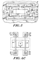
- FIG. 5 An alternative electrode arrangement for a micromechanical gyroscopic transducer, according to the invention, is illustrated in Fig. 5.
- four buried electrodes are configured in combination with two surface bridge electrodes one each replacing a pair 58/60 and 62/64 of Fig. 1, to effect the micromechanical gyroscopic transduction function as described hereinbefore.
- Outer buried electrodes 118,120 are disposed below outer gimbal plate 32 parallel to the axis formed by the flexures 20,22 and serve as torquing electrodes providing the function of driving outer gimbal plate 32 at one frequency, sensing the displacement at a second frequency and controlling the first frequency drive to achieve a controlled vibration as described in the referenced application.
- Inner buried electrodes 122,124 are disposed between buried electrodes 118,120 and loop beneath opposite ends of plate 34 from opposite ends of transducer element 18.
- Inner buried electrodes 112,124 provide the function of rebalance torquing, with a drive voltage, typically 1.0 mV, which rebalances or drives to null inner gimbal plate 34 with mass 48.
- Inner buried electrodes 122,124 have cutouts 126,128 around the region of flexures 20,22.
- two surface bridge electrodes are configured as discussed hereinbefore with respect to the four bridge electrodes of Fig. 1.
- four bridge electrodes were configured in proximity to inner gimbal plate 34, two on either side of balanced mass 48, parallel to the Y-axis defined by first and second ends of flexures 36,38, in the embodiment of Fig. 5
- only one bridge electrode is configured on either side of balanced mass 48, parallel to the Y-axis and in proximity to inner gimbal plate 34.
- the two bridge electrodes are used to sense inner gimbal plate 34 motion, while an excitation frequency is applied through flexures to the inner gimbal plate 34.
- the bridge electrode may be located to provide vertical symmetry with respect to the rebalance torquing buried electrodes 122,124.
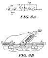
- FIG. 6A Shown in Fig. 6A is electrical circuitry for on-chip signal processing to limit the effect of parasitic capacitance in long signal paths in an embodiment wherein an excitation frequency is applied to inner gimbal plate 34 through bridge or buried electrodes and a signal indicating inner gimbal 34 motion is sensed at a flexure node 200.
- An electrical equivalent circuit diagram, illustrated in Fig. 6B, of the micromechanical gyroscopic transducer capacitances includes capacitances C 1 -C n and Cp wherein C 1 -C n represent the variable capacitances resulting from the distance of the inner gimbal plate 34 relative to n excited buried and bridge electrodes.
- the resulting signal at the gimbal plate 34 is sensed through flexures and outer gimbal plate 32 to frame 16.
- a parasitic capacitance Cp between the structure 18 and the semiconductor mass 12 acts as a shunt and is large enough to reduce the signal to noise ratio particularly if it includes any length of signal path prior to impedance buffering.
- the gimbal signal is buffer amplified by an on-chip JFET which minimizes the effect of shunt capacitance from long lead lengths by reducing the impedance of the signal for application to off-chip electronics 55 as described in the above-referenced application to provide the signals necessary to electronically torque the instrument and derive rate outputs.
- the signal from the inner gimbal 34 is present at output node 200 which is connected to the gate of a high input impedance JFET Q 1 which is fabricated on-chip and proximate to the signal source as an impedance buffering preamplifier to overcome the effects of parasitic capacitance.
- Transistor Q 2 is fabricated along with Q 1 as a matched pair.
- amplifier A 1 on- or off-chip
- it serves to bias the gate of Q 1 at a virtual ground. This provides a stable reference for the torque electrodes shown as C n .
- Electronics 55 provides the drive signals for capacitors C 1 through C n , the biases for R 1 and the drains of Q 1 and Q 2 .
- Amplifier A 1 is typically a unity voltage gain high gain amplifier providing feedback to an on-chip RC combination R 1 and C 10 which provides signal stabilization.
- the output of operational amplifier A 1 is processed by electronics 55.
- the on-chip JFET buffer amplifier Q 1 is fabricated on the chip in proximity to a flexure frame junction to ensure minimum parasitic capacitance and high stability.
- the RC combination of R 1 and C 10 may also be provided on-chip.
- R 1 may be fabricated in the megohm range from polysilicon or it may be formed on-chip as a biased JFET as shown in Fig. 6B.
- C 10 may be a MOS device fabricated on-chip.
- the p regions 150 doped to act as sources and drain (the p channel 152 and the gate 154 being diffused separately) in the on-chip JFETs may be fabricated as highly doped regions during the boron doping process steps used to make flexure and gimbal plate etch resistant structures as discussed hereinbefore or in separate steps.
- Metalliza- tions 156 and 158 for the source and drain and for gate 154, respectively required for electrical contact to the on-chip JFET can be provided during metallization process steps undertaken during the fabrication of the micromechanical gyroscopic transducer structure as described in the above.
- Metalization 154 extends to an aperture in layer 160 where it contacts a doped flexure to the outer gimbal plate.
- An embodiment wherein an excitation frequency is applied to inner gimbal 34, as illustrated in Fig. 4C, may provide a better signal-to-noise ratio when the signal indicating inner gimbal 34 motion is sensed differentially by a pair of surface bridge electrodes 58,64.
- Surface bridge electrodes as discussed in the referenced application, can provide lower capacitance than buried electrodes and can be electrically isolated by driven shields provided at the bridge electrode landings 106 as discussed hereinbefore with respect to Figs. 4, 4A, 4B and 4C.
- An electrical model of such a configuration and an illustration of a JFET buffer preamplifier located proximate to the bridge electrode landing are shown in Figs. 6C and 6D, respectively.
- a high frequency approximately 100 kHz signal is inserted on inner gimbal plate 34 by electronics 55.
- Bridges 64 and 58 serve as a differential capacitive pickoff. Areas 110,110a of the bridges have relatively high capacitance to the electrically isolated regions 111,111a.
- the differential signals from C 1 and C 2 are fed to the gates of JFETs Q 1 and Q 1a which serve as buffer amplifiers to greatly lower the signal impedance and isolate it from electrical interference.
- Transistors Q 2 and Q 2a and external electronics 55 (not shown in Fig. ) form a biasing network for the gates of Q 1 and Q 1a .
- Amplifier A 1 is a differential amplifier (either on- or off-chip) which differences and amplifies the positional signal.
- Nodes N 1 and N 1a are low impedance reference nodes which track the gate voltage in phase and amplitude and which may be used to drive regions 111 and 111a thereby effectively neutralizing the parasitic capacitance from regions 110,110a to 111,111a. The result is a greater signal-to-noise ratio.
Landscapes
- Physics & Mathematics (AREA)
- Engineering & Computer Science (AREA)
- General Physics & Mathematics (AREA)
- Radar, Positioning & Navigation (AREA)
- Remote Sensing (AREA)
- Gyroscopes (AREA)
- Bipolar Transistors (AREA)
Abstract
Description
- This invention relates to gyroscopic transducers and, in particular to gyroscopic transducers manufactured using semiconductor fabrication processes.
- Semiconductor fabrication techniques are in use to produce micromechanical structures from silicon wafers. Such micromechanical structures have the potential of mass production at a very low cost.
- Illustrative of this particular technology is U.S. Patent No. 4,598,585 to Boxenhorn, which discloses a planar micromechanical vibratory gyroscope adapted for small geometry configurations which may be constructed using semiconductor fabrication mass production techniques.
- Further advances in micromechanical gyroscopic transducer technology are described in Applicant's co-pending U.S. Patent Application Serial No. 07/143,515, filed January 13, 1988, entitled METHOD AND APPARATUS FOR SEMICONDUCTOR CHIP TRANSDUCER and U.S. Application Serial No. 07/143,515, Filed January 13, 1988, entitled METHOD AND APPARATUS FOR SEMICONDUCTOR CHIP TRANSDUCER.
- Other advances in micromechanical gyroscopic technology are described in Applicant's pending U.S. Patent Application US-A-5 216 490 entitled BRIDGE ELECTRODES.
- The infancy of monolithic micromechanical semiconductor gyroscopic transduction technology assures that significant advances will continue to be made with respect to implementation and application of the technology. As structures are implemented having increased sensitivity and accuracy, problem areas are identified and solutions defined. Presently, shortcomings with respect to "rippling" of an oxide support frame from which an outer flexure extends connecting a resonating structure thereto are observable. "Buckling" of inner flexures, results in undesirable large variations in a critical resonant frequency of a suspended gyroscopic element. Furthermore, surface bridge electrodes used for sensing and for rebalancing of a certain axis of a resonating structure have large capacitances to the substrate limiting effectiveness as signal pickoffs.
- Further document US-A-4 699 006 discloses further details of such monolithic semiconductor designs in accelerometers and gyroscopes. This document in particular details a gyroscope which basically comprises a semiconductor mass with a recess, above which is positioned a transducer element with first and second gimballed plates integrally linked to the mass, respectively the first plate via flexing links. The second plate bears a balanced mass, and sets of electrodes are provided in, i.e. integral to the semiconductor mass.
- Prior art document Sensors and Actuators, A21-A23, Feb'90, Elsevier Sequoia (NL), pp 273-277; Boxenhorn et al.: "Monolithic Silicon Accelerometer" describes further developments in design and manufacture of monolithic silicon micromechanical accelerometers. This document in particular suggests the use of bridge electrodes spanning the gimbal plate of the accelerometer, in order to produce more symmetrical torquing and better linearity.
- The above problems are solved by a gyroscope having the features of
claim 1. - The invention will be more fully understood from the following detailed description of illustrative embodiments taken in conjunction with the accompanying drawing in which:
- Fig. 1 is a perspective view partially cut away of a semiconductor chip gyroscopic transducer according to the invention;
- Fig. 2 is an expanded view of a semiconductor chip gyroscopic transducer flexure/frame junction with a footing according to the invention;
- Fig. 2A is an expanded side view of a P-type footing disposed at the flexure/frame junction of Fig. 2;
- Fig. 3 is a conceptual view of a semiconductor chip gyroscopic transducer having a strain relief and torsional stiffness system and footings according to the invention;
- Fig. 3A is a side sectional view of flexure grooves according to the invention, formed by plasma etching
- Fig. 3B is a side sectional view of flexure grooves according to the invention, formed by anisotropic etching;
- Fig. 4 is a cross-section view of the semiconductor chip gyroscopic transducer of Fig. 1 taken along a line Y-Y;
- Fig. 4A is a top view of an electrically isolated bridge electrode landing;
- Fig. 4B is a side section view of the isolated landing of Fig. 4A;
- Fig. 4C is a top, diagrammatic view of a micromechanical gyroscopic transducer having signal pickoff by inner bridge electrodes with electrically isolated landings;
- Fig. 5 is an alternative embodiment of a semiconductor chip gyroscopic transducer having four buried electrodes and two bridge electrodes according to the invention;
- Fig. 6A is a side section and perspective view of a micromechanical gyroscopic transducer having an on-chip JFET buffer for amplifying a signal picked off of a flexure;
- Fig. 6B is a schematic diagram of a micromechanical gyroscopic transducer including the on-chip JFET buffer amplifier of Fig. 6A;
- Fig. 6C is a schematic diagram of electronic circuitry for the gyroscopic transducer of Fig. 4C having bridge electrode signal pickoff; and
- Fig. 6D is a side section and perspective view of a micromechanical gyroscopic transducer having on-chip JFET buffer circuitry in proximity to pickoff bridge electrodes.
- A micromechanical
gyroscopic transducer 10, as viewed in Fig. 1, is formed from a mass of N-type silicon 12.Mass 12 is preferably an N-type epitaxially grown layer 13 on a base of monocrystalline N-type silicon 15. Selective etching of thesilicon 12 as described in the above-referenced applications yields avoid 14 within asilicon frame 16. Atransducer element 18, which has been doped P-type and is freed fromsilicon mass 12 as a result of selective etching is suspended above thevoid 14. Thetransducer element 18, comprising outer andinner portions flexures portion 32 oftransducer element 18 to thesilicon frame 16.Flexures first ends silicon frame 16.Second ends flexures gimbal plate 32 of thetransducer element 18.First gimbal plate 32 flexibly supported byflexures flexures - Interior to
gimbal plate 32 oftransducer element 18 is the second portion, or asecond gimbal plate 34. A second set offlexures second gimbal plate 34 to thefirst gimbal plate 32.Second flexures first ends second ends first ends flexures first gimbal plate 32. Thesecond ends second gimbal plate 34.Second gimbal plate 34 is capable of limited rotation about a Y-axis, orthogonal to the X-axis, extending through thefirst ends second ends flexures Second gimbal plate 34 supports a centrally locatedmass 48 which is substantially balanced between top and bottom of thesecond gimbal plate 34. Substantiallybalanced mass 48 is formed onsecond gimbal plate 34 by selectively etching a trough therein. The process, discussed in significant detail in above-referenced U.S. Patent Application Serial No. 143,515, includes provision of a deep pit, through the surface ofsilicon mass 12 wheremass 48 is to be located, prior to etch resistant doping of theplate 34. After etching, the pit remains and may be filled with single crystal or polysilicon followed by a solid electroplating on a layer of titanium tungsten (TiW) covered with a layer of gold (Au) deposited via vacuum deposition. A mass of gold may alternatively be electroplated into the pit on the layer of vacuum deposited gold. A Z-axis is defined by the central location of the topside and bottomside of the substantiallybalanced mass 48. The process of metal plating on silicon is discussed below. - In the illustrative embodiment of Fig. 1, the micromechanical
gyroscopic transducer 10 has four integral or buriedelectrodes first gimbal plate 32 substantially parallel to the X-axis. The buriedelectrodes base layer 15 prior to the growth of epitaxial layer 13. With the typically N-type silicon mass these form P-N junctions. Typically, two of the electrodes are used for torquing thetransducer element 18 and two are used for sensing and vibration angle amplitude control. Buried electrode functionality is facilitated by electrical connection through a deep P+ diffusion to the buried electrodes which are in turn surface metallized and connected tocontacts frame 16 which are in turn electrically connected to associated on- or off-chip drive andsense electronics 55 onsignal bus 57 that cause controlled amplitude vibration ofplate 32 as discussed below. - Additionally, the micromechanical
gyroscopic transducer 10 has foursurface bridging electrodes transducer element 18 and are bonded tosilicon frame 16 atrespective electrode landings bridge electrodes second gimbal plate 34, two each on either side of substantiallybalanced mass 48, parallel to the Y-axis defined by first and second ends offlexures plate 34. For this purpose, they are connected to signalbus 57 andelectronics 55. Bridge electrodes are fabricated using metal plating technology discussed in the referenced application. - Functionally, the
second gimbal plate 34 with substantiallybalanced mass 48 supported byflexures First gimbal plate 32 is a driven member which is caused to vibrate at a fixed frequency and angular amplitude about the X-axis. The fixed frequency of vibration with which thefirst gimbal plate 32 is driven is the resonant frequency of thesecond gimbal plate 34 with substantiallybalanced mass 48. Vibration of thefirst gimbal plate 32 is induced by applying appropriate alternating DC voltages to the outer buriedelectrodes electrodes first gimbal plate 32 vibration angle amplitude.Electronics 55 provides feedback control over the torque to insure a fixed amplitude. The torque electrodes are preferably buried for stability. The resulting dynamical system is sensitive to rotation of the structure about a Z-axis orthogonal to the X and Y axes and passing through thebalanced mass 48. When rotation of the system about the Z-axis occurs,second gimbal plate 34 with substantiallybalanced mass 48 oscillates at its resonant frequency at an amplitude proportional to the rate of rotation applied. -
Surface bridge electrodes transducer element 18 in proximity tosecond gimbal plate 34 are used for sensing and for rebalance of thesecond gimbal plate 34 with substantiallybalanced mass 48, nulling its tendency to vibrate. Because the gyro described hereinbefore in an open loop condition is very sensitive to parameter variations such as small changes in the resonant frequency ofsecond gimbal plate 34 or small changes in the angle of vibration, it is a practical necessity to operate the gyro in a closed loop condition to minimize this sensitivity. Closed loop operation requires that the gyro be incorporated into a rebalance loop that maintainssecond gimbal plate 34 at null by torquing thesecond gimbal plate 34 electrostatically. By torquingsecond gimbal plate 34 null the gyro system can tolerate variations in vibration frequency. Closed loop operation enables the drive vibration angle amplitude offirst gimbal plate 32 to be increased without cross-coupling interactions with thesecond gimbal plate 34, sincesecond gimbal plate 34 is maintained near null by closed loop rebalancing. - Closed loop rebalancing is facilitated by two quadrature servo-loops in
electronics 55 operating in conjunction. The servo-control electronics, as shown in the referenced application, will rebalancesecond gimbal plate 34 so that the effect on nonorthogonality of the gimbals and the unbalance of thesecond gimbal plate 34 will be minimized. The output of thecontrol electronics 55 is a voltage proportional to the torque required to rebalance thesecond gimbal plate 34 against gyroscopic torques. A third servo-controlled loop is required to maintain vibration drive angle offirst gimbal plate 32 at a fixed value. The third servo-control loop is similar to the control loops ofsecond gimbal plate 34 but allows a much lower bandwidth. - The desirability of surface bridge electrodes as opposed to an increased number of integral or buried electrodes, results from a large voltage dependent parasitic capacitance to the
semiconductor mass 12 inherent in such buried electrodes. Furthermore, buried electrodes exhibit a small leakage current and are limited with respect to the voltage which can be applied, that being the reverse breakdown voltage of a P-N junction, typically about 40 volts. Buried electrode utility is also limited in a micromechanical gyroscopic transducer application since although they can be disposed in a manner parallel to an X-axis of rotation of the first gimbal plate they cannot concurrently be disposed in a manner perpendicular to that same axis of rotation (or parallel to a Y-axis of rotation of the second gimbal plate). Because surface bridge electrodes can be disposed perpendicular to buried electrodes, the surface bridge electrodes can be aligned in proximity and parallel to the axis of rotation ofsecond gimbal plate 34 while buried electrodes are aligned in proximity and parallel to the axis of rotation offirst gimbal plate 32. A single pair of bridge electrodes can replace thedouble pair - In the selective etching of
void 14, whereinsilicon frame 16, thedouble gimbal plates adjacent flexures unsupported lip 82 which is subject to rippling (Fig. 2). The geometric variations induced by rippling along thelip 82 causes a variation in twist onflexures transducer element 18 insilicon frame 16. The resultant twisting forces exerted on theflexures first gimbal plate 32 which consequently affects the gyroscopic sensitivity ofsecond gimbal plate 34. The detrimental effect of the rippling of thesilicon dioxide lip 82 which is typically 0.6 micron in thickness at the undercut, according to the invention, is prevented by employing a 3 micron P-type diffusion orfooting 84 at the junction offlexures silicon frame 16. The disposition offooting 84 is best viewed in Fig. 2A. It can be seen that N-type silicon frame 16 has disposed therein P-type footing 84 at the junction ofsilicon frame 16 andflexures flexures void 14. P-type footing 84 acts as a buffer between rippledportions 82 precluding the twisting which otherwise results, while maintaining P-N junction isolation of the double gimbal double flexure transducer fromsilicon frame 16. - Referring now to Fig. 3, a double flexure double gimbal plate micromechanical gyroscopic transducer is provided, in combination, with a strain relief and torsional stiffness system. This is provided by grooved flexures and strain relieving slots defining tension relief beams at the junction of the flexures and
outer gimbal plate 32. - As shown there,
gimbal plate 32 has disposed therein fourslots Slots flexures tension relief beams flexures plate 32.Slots flexures join plate 32 and form beams 96 and 100. - The
outer gimbal 32 is in tension because its etch resistance results from boron doping which reduces the lattice spacing with respect to the surrounding N-type dopedmass 12. The result is that the undercut structure tries to shrink but is restrained by the largerstiffer mass 12 and this putsgimbal plate 32 in tension. In the axis throughflexures gimbal 32 is thicker than theflexures rate putting flexures Beams plate 32 also affects the resonant frequency ofgimbal plate 32. By trimming the slot and beam sizes the resonant frequency can be controlled. Trimming beams 96,100, provides compression relief as discussed above. -
Grooves flexures stress relieving beams 96 and 100 impact the torsional dynamics of the second flexible linkage means,grooves flexures flexures - Figs. 3A and 3B illustrate the construction of such a groove. Pits 102,104 are formed by a plasma or other etching process, as known in the art, prior to the P-type diffusion that defines the flexures. The diffusion thus takes the form of a groove or channel, providing box beam stiffening.
- Referring now to Fig. 4, there is shown a cross-sectional view of the micromechanical gyroscopic transducer, according to the invention. A
bridge electrode 64 is shown and is constructed in a manner described in U.S. Patent Application Serial No. 372,653 entitled BRIDGE ELECTRODES. Anotherbridge electrode 58 is located behindelectrode 64 and therewith span thetransducer element 18 above thesecond gimbal plate 34, a few microns therefrom. - Each bridge electrode has opposite landings or terminations represented by landings 106,108 illustrated in Figs. 4, 4A, 4B and 4C, disposed on the
silicon frame 16. The electrode landings are formed overmetallization layer 110. An oxide layer 113- provides DC electrical isolation but capacitance to substrate is still large. In some cases (i.e. where the bridge electrodes are used at high impedance for signal pickoff instead of excitation from a low impedance source) this capacitance adversely affects the signal. - The construction illustrated in Figs. 4A and 4B provides a driven shield to effectively neutralize this capacitance. As shown also in Fig. 4C electrical isolation regions 111 and 111a are provided under the landings of the signal pickoff bridges 64 and 58. In the discussion to follow it is understood that both regions 111, on both sides of the bridge, are treated the same electrically. This is true of regions 111a as well. Regions 111 and 111a are DC isolated by the surrounding P regions 112,114. By circuitry described below and illustrated in Fig. 6C, the region 111 is driven at the same (or nearly the same) potential as
electrode landing 106 and the capacitance between them is thus electrically neutralized, maximizing the signal-to-noise ratio at the point of pickoff. - An alternative electrode arrangement for a micromechanical gyroscopic transducer, according to the invention, is illustrated in Fig. 5. In this embodiment four buried electrodes are configured in combination with two surface bridge electrodes one each replacing a
pair 58/60 and 62/64 of Fig. 1, to effect the micromechanical gyroscopic transduction function as described hereinbefore. - Outer buried electrodes 118,120 are disposed below
outer gimbal plate 32 parallel to the axis formed by theflexures outer gimbal plate 32 at one frequency, sensing the displacement at a second frequency and controlling the first frequency drive to achieve a controlled vibration as described in the referenced application. - Inner buried electrodes 122,124, are disposed between buried electrodes 118,120 and loop beneath opposite ends of
plate 34 from opposite ends oftransducer element 18. Inner buried electrodes 112,124 provide the function of rebalance torquing, with a drive voltage, typically 1.0 mV, which rebalances or drives to nullinner gimbal plate 34 withmass 48. Inner buried electrodes 122,124 have cutouts 126,128 around the region offlexures - In this embodiment, two surface bridge electrodes, not shown, are configured as discussed hereinbefore with respect to the four bridge electrodes of Fig. 1. However, whereas four bridge electrodes were configured in proximity to
inner gimbal plate 34, two on either side ofbalanced mass 48, parallel to the Y-axis defined by first and second ends offlexures balanced mass 48, parallel to the Y-axis and in proximity toinner gimbal plate 34. The two bridge electrodes are used to senseinner gimbal plate 34 motion, while an excitation frequency is applied through flexures to theinner gimbal plate 34. The bridge electrode may be located to provide vertical symmetry with respect to the rebalance torquing buried electrodes 122,124. - Shown in Fig. 6A is electrical circuitry for on-chip signal processing to limit the effect of parasitic capacitance in long signal paths in an embodiment wherein an excitation frequency is applied to
inner gimbal plate 34 through bridge or buried electrodes and a signal indicatinginner gimbal 34 motion is sensed at aflexure node 200. An electrical equivalent circuit diagram, illustrated in Fig. 6B, of the micromechanical gyroscopic transducer capacitances includes capacitances C1-Cn and Cp wherein C1-Cn represent the variable capacitances resulting from the distance of theinner gimbal plate 34 relative to n excited buried and bridge electrodes. The resulting signal at thegimbal plate 34 is sensed through flexures andouter gimbal plate 32 to frame 16. A parasitic capacitance Cp between thestructure 18 and thesemiconductor mass 12 acts as a shunt and is large enough to reduce the signal to noise ratio particularly if it includes any length of signal path prior to impedance buffering. For this purpose the gimbal signal is buffer amplified by an on-chip JFET which minimizes the effect of shunt capacitance from long lead lengths by reducing the impedance of the signal for application to off-chip electronics 55 as described in the above-referenced application to provide the signals necessary to electronically torque the instrument and derive rate outputs. - As illustrated in Fig. 6B the signal from the
inner gimbal 34 is present atoutput node 200 which is connected to the gate of a high input impedance JFET Q1 which is fabricated on-chip and proximate to the signal source as an impedance buffering preamplifier to overcome the effects of parasitic capacitance. Transistor Q2 is fabricated along with Q1 as a matched pair. In connection with amplifier A1 (on- or off-chip), it serves to bias the gate of Q1 at a virtual ground. This provides a stable reference for the torque electrodes shown as Cn. Electronics 55 provides the drive signals for capacitors C1 through Cn, the biases for R1 and the drains of Q1 and Q2. Amplifier A1 is typically a unity voltage gain high gain amplifier providing feedback to an on-chip RC combination R1 and C10 which provides signal stabilization. The output of operational amplifier A1 is processed byelectronics 55. - As illustrated in Fig. 6A the on-chip JFET buffer amplifier Q1 is fabricated on the chip in proximity to a flexure frame junction to ensure minimum parasitic capacitance and high stability. Furthermore, the RC combination of R1 and C10 may also be provided on-chip. R1 may be fabricated in the megohm range from polysilicon or it may be formed on-chip as a biased JFET as shown in Fig. 6B. C10 may be a MOS device fabricated on-chip. The
p regions 150 doped to act as sources and drain (thep channel 152 and the gate 154 being diffused separately) in the on-chip JFETs may be fabricated as highly doped regions during the boron doping process steps used to make flexure and gimbal plate etch resistant structures as discussed hereinbefore or in separate steps. Metalliza-tions layer 160 where it contacts a doped flexure to the outer gimbal plate. - An embodiment wherein an excitation frequency is applied to
inner gimbal 34, as illustrated in Fig. 4C, may provide a better signal-to-noise ratio when the signal indicatinginner gimbal 34 motion is sensed differentially by a pair ofsurface bridge electrodes bridge electrode landings 106 as discussed hereinbefore with respect to Figs. 4, 4A, 4B and 4C. An electrical model of such a configuration and an illustration of a JFET buffer preamplifier located proximate to the bridge electrode landing are shown in Figs. 6C and 6D, respectively. - Referring to Figs. 6C and 6D, a high frequency approximately 100 kHz signal is inserted on
inner gimbal plate 34 byelectronics 55.Bridges - Although the invention has been shown and described with respect to exemplary embodiments thereof various other changes, omissions and additions in form and detail thereof may be made therein without departing from the scope of the invention as defined in the appended claims.
Claims (33)
- A micromechanical gyroscopic transducer comprising:a mass (12) of semiconductor material having a void (14) on a top surface extending downward, said mass of silicon comprising a silicon frame (16);a transducer element (18) suspended above said void (14), said transducer element (18) comprising:first and second flexible linkages (20, 22) integral with said frame material (16) for coupling said transducer element to said frame (16) at opposite ends, first ends (24, 26) of said first flexible linkages (20, 22) being connected to said silicon frame (16);a first gimbal plate (32) integral with said frame material (16) connected to said second ends (28, 30) of said first and second flexible linkages (20, 22), said first gimbal plate (32) being capable of oscillatory motion about an axis through said first and second flexible linkages (20, 22);a second gimbal plate (34), interior to said first gimbal plate (32);third and fourth flexible linkages (36, 38) integral with said frame material (16) coupling said second gimbal plate (34) to said first gimbal plate (32) on opposite ends, said third and fourth flexible linkages (36, 38) having first ends (40, 42) and second ends (44, 46), said first ends of said third and fourth flexible linkages (36, 38) being connected to said first gimbal plate (32) and said second ends of said third and fourth flexible linkages (36, 38) being connected to said second gimbal plate (34), said second gimbal plate (34) being capable of oscillatory motion about an axis through said third and fourth flexible linkages (36, 38);a substantially balanced mass (48), central to said second gimbal plate (34), said substantially balanced mass (48) having a top side and a bottom side defining an axis therebetween;first and second sets of electrodes (50, 52, 54, 56) configured within said mass (12) in a bottom region of said void (14) and integral with said frame material, said first set of integral electrodes facing said first gimbal plate (32) and said second set of integral electrodes facing said second gimbal plate (34);characterized in thata plurality of bridge electrodes (58, 60, 62, 64) are configured above said transducer element (18), each of said plurality of bridge electrodes (58, 60, 62, 64) being supported from said frame (16) at an electrode landing (106, 108) and extending over at least one of said first (32) and second (34) gimbal plates,each of said bridge electrodes (58, 60, 62, 64) are supported from said frame on a region of doped material (111, 112, 114) disposed between and in electrical communication with said bridge electrodes (58, 60, 62, 64) and said mass material (12)wherein said region of doped material (111, 112, 114) comprises an intermediate area (111) isolated by surrounding areas (112, 114), said intermediate area (111) in use being biased relative to said mass material (12) so as to effectively isolate said bridge electrodes (58, 60, 62, 64) from said mass material (12).
- The micromechanical gyroscopic transducer of claim 1,
characterized in that
said mass (12) is monocrystalline silicon (15) and said void (14) is anisotropically etched therein. - The micromechanical gyroscopic transducer of claim 2,
characterized in that
said first and second gimbal plates (32, 34) include etch resistant dopants and are formed by selective etching of said mass (12). - The micromechanical gyroscopic transducer of claim 1,
characterized in that
said flexible linkages (20, 22, 36, 38) include etch resistant dopants and are formed by selective etching of said mass (12). - The micromechanical gyroscopic transducer of claim 1,
characterized in that
said first gimbal plate (32) includes means (94, 96, 98, 100) for relieving stress adjacent one or more of said flexible linkages (20, 22, 36, 38). - The micromechanical gyroscopic transducer of claim 5,
characterized in that
said means for relieving stress comprises a beam (94, 96, 98, 100) created by a slot (86, 88, 90, 92). - The micromechanical gyroscopic transducer of claim 6,
characterized in that
said slot (86, 90) is proximate to said second ends of said first and second flexible linkages (20, 22). - The micromechanical gyroscopic transducer of claim 6,
characterized in that
said slot (86, 90) is orthogonally disposed with respect to said axis of said first and second flexible linkages (20, 22). - The micromechanical gyroscope transducer of claim 6,
characterized in that
said slot (88, 92) is proximate to said first ends of said third and fourth flexible linkages (36, 38). - The micromechanical gyroscopic transducer of claim 6,
characterized in that
said slot (88, 92) is orthogonally disposed with respect to said axis of said third and fourth flexible linkages (36, 38). - The micromechanical gyroscopic transducer of claims 6, 7 or 8,
characterized in that
said slot (86, 90) is trimmed to adjust a beam (94, 98) formed by said slot, said beam defining a resonant frequency of said first gimbal plate (32) as supported by said first and second flexible linkages (20, 22). - The micromechanical gyroscopic transducer of claims 6, 9 or 10,
characterized in that
said slot (88, 92) is trimmed to adjust a beam (96, 100) formed by said slot, said beam defining a resonant frequency of said second gimbal plate (34). - The micromechanical gyroscopic transducer of claim 1,
characterized in that
at least two opposite ones of said flexible linkages (36, 38) further include a depressed portion (102, 104) extending in a direction parallel to the axis defined by said opposite linkages to stiffen said linkages against buckling and bending without corresponding torsional stiffening. - The micromechanical gyroscopic transducer of claim 13,
characterized in that
said depressed portion (102, 104) is formed by plasma etching. - The micromechanical gyroscopic transducer of claim 13,
characterized in that
said depressed portion (102, 104) is formed in said flexible linkages (36, 38) by anisotropic etching. - The micromechanical gyroscopic transducer of claim 1,
characterized in that
said first and second flexible linkages (20, 22, 36, 38) join said frame (16) at a footing region (84) of doped material which region being beyond said first ends of said first and second flexible linkages to reduce twisting thereof. - The micromechanical gyroscopic transducer of claim 16,
characterized in that
said footing region (84) is a P-type material. - The micromechanical gyroscopic transducer of claim 1,
characterized in that
said substantially balanced mass (48) comprises a gold plated top portion extending above said void (14). - The micromechanical gyroscopic transducer of claim 18,
characterized in that
said balanced mass (48) includes a polysilicon portion under said gold top portion. - The micromechanical gyroscopic transducer of claim 18,
characterized in that
said balanced mass (48) includes a single crystal silicon portion under said gold top portion. - The micromechanical gyroscopic transducer of claim 18,
characterized in
having a titanium tungsten metal layer below said gold. - The micromechanical gyroscopic transducer of claim 21,
characterized in
having a gold layer above the titanium tungsten layer. - The micromechanical gyroscopic transducer of claim 22,
characterized in that
said titanium tungsten and gold layers are deposited by vacuum deposition. - The micromechanical gyroscopic transducer of claim 18,
characterized in that
said gold mass is plated on said second metal by electroplating. - The micromechanical gyroscopic transducer of claim 1,
characterized in that
said integral electrodes (50, 52, 54, 56) are formed as a highly doped P-type region patterned on an N-type silicon sub-surface. - The micromechanical gyroscopic transducer of claim 25,
characterized in that
said void (14) is in an N-type layer epitaxially grown over said sub-surface. - The micromechanical gyroscopic transducer of claim 1,
characterized in that
said integral electrodes (50, 52, 54, 56) are electrically connected through a doped region to a metallized contact on said silicon frame (16). - The micromechanical gyroscopic transducer of claim 1,
characterized in that
said bridge electrodes (58, 60, 62, 64) are configured above and facing said second gimbal plate (34). - The micromechanical gyroscopic transducer of claim 1,
characterized in that
said region of doped material (111, 112, 114) comprises an isolating wall (114), an isolating floor (112) and an isolating intermediate area (111) and a driven shield. - The micromechanical gyroscopic transducer of claim 29,
characterized in that
said isolating wall (114) and said isolating floor (112) comprise P-type doped semiconductor material. - The micromechanical gyroscopic transducer of claim 29,
characterized in that
said isolating intermediate area (111) is an N-type semiconductor material. - The micromechanical gyroscopic transducer of claim 1,
characterized in
further comprising a junction field effect transistor (Q1) fabricated in said semiconductor mass (12). - The micromechanical gyroscopic transducer according to one of the preceding claims,
characterized in that
said gimbal plates (32, 34) are thicker than said flexible linkages (20, 22, 36, 38).
Applications Claiming Priority (3)
| Application Number | Priority Date | Filing Date | Title |
|---|---|---|---|
| US493327 | 1990-03-14 | ||
| US07/493,327 US5016072A (en) | 1988-01-13 | 1990-03-14 | Semiconductor chip gyroscopic transducer |
| PCT/US1991/001702 WO1991014285A1 (en) | 1990-03-14 | 1991-03-14 | Semiconductor chip gyroscopic transducer |
Publications (3)
| Publication Number | Publication Date |
|---|---|
| EP0472717A1 EP0472717A1 (en) | 1992-03-04 |
| EP0472717A4 EP0472717A4 (en) | 1992-08-19 |
| EP0472717B1 true EP0472717B1 (en) | 1997-06-04 |
Family
ID=23959783
Family Applications (1)
| Application Number | Title | Priority Date | Filing Date |
|---|---|---|---|
| EP91906925A Expired - Lifetime EP0472717B1 (en) | 1990-03-14 | 1991-03-14 | Semiconductor chip gyroscopic transducer |
Country Status (7)
| Country | Link |
|---|---|
| US (1) | US5016072A (en) |
| EP (1) | EP0472717B1 (en) |
| JP (1) | JPH05502945A (en) |
| AT (1) | ATE154166T1 (en) |
| CA (1) | CA2057919C (en) |
| DE (1) | DE69126381T2 (en) |
| WO (1) | WO1991014285A1 (en) |
Families Citing this family (139)
| Publication number | Priority date | Publication date | Assignee | Title |
|---|---|---|---|---|
| US5216490A (en) * | 1988-01-13 | 1993-06-01 | Charles Stark Draper Laboratory, Inc. | Bridge electrodes for microelectromechanical devices |
| DE4000903C1 (en) * | 1990-01-15 | 1990-08-09 | Robert Bosch Gmbh, 7000 Stuttgart, De | |
| US5144184A (en) * | 1990-01-26 | 1992-09-01 | The Charles Stark Draper Laboratory, Inc. | Micromechanical device with a trimmable resonant frequency structure and method of trimming same |
| US5126812A (en) * | 1990-02-14 | 1992-06-30 | The Charles Stark Draper Laboratory, Inc. | Monolithic micromechanical accelerometer |
| US5473945A (en) | 1990-02-14 | 1995-12-12 | The Charles Stark Draper Laboratory, Inc. | Micromechanical angular accelerometer with auxiliary linear accelerometer |
| DE69102590T2 (en) * | 1990-05-18 | 1994-10-06 | British Aerospace | Inertial sensors. |
| US6729545B2 (en) * | 1990-05-29 | 2004-05-04 | Symbol Technologies, Inc. | Integrated scanner on a common substrate having an omnidirectional mirror |
| DE4022495A1 (en) | 1990-07-14 | 1992-01-23 | Bosch Gmbh Robert | MICROMECHANICAL SPEED SENSOR |
| US5314572A (en) * | 1990-08-17 | 1994-05-24 | Analog Devices, Inc. | Method for fabricating microstructures |
| JPH0644008B2 (en) * | 1990-08-17 | 1994-06-08 | アナログ・ディバイセス・インコーポレーテッド | Monolithic accelerometer |
| US5326726A (en) * | 1990-08-17 | 1994-07-05 | Analog Devices, Inc. | Method for fabricating monolithic chip containing integrated circuitry and suspended microstructure |
| US5417111A (en) * | 1990-08-17 | 1995-05-23 | Analog Devices, Inc. | Monolithic chip containing integrated circuitry and suspended microstructure |
| US5408119A (en) * | 1990-10-17 | 1995-04-18 | The Charles Stark Draper Laboratory, Inc. | Monolithic micromechanical vibrating string accelerometer with trimmable resonant frequency |
| US5605598A (en) * | 1990-10-17 | 1997-02-25 | The Charles Stark Draper Laboratory Inc. | Monolithic micromechanical vibrating beam accelerometer with trimmable resonant frequency |
| US5205171A (en) * | 1991-01-11 | 1993-04-27 | Northrop Corporation | Miniature silicon accelerometer and method |
| US5241861A (en) * | 1991-02-08 | 1993-09-07 | Sundstrand Corporation | Micromachined rate and acceleration sensor |
| US5129983A (en) * | 1991-02-25 | 1992-07-14 | The Charles Stark Draper Laboratory, Inc. | Method of fabrication of large area micromechanical devices |
| US5203208A (en) * | 1991-04-29 | 1993-04-20 | The Charles Stark Draper Laboratory | Symmetrical micromechanical gyroscope |
| US5121180A (en) * | 1991-06-21 | 1992-06-09 | Texas Instruments Incorporated | Accelerometer with central mass in support |
| US5635639A (en) * | 1991-09-11 | 1997-06-03 | The Charles Stark Draper Laboratory, Inc. | Micromechanical tuning fork angular rate sensor |
| US5331852A (en) * | 1991-09-11 | 1994-07-26 | The Charles Stark Draper Laboratory, Inc. | Electromagnetic rebalanced micromechanical transducer |
| US5313835A (en) * | 1991-12-19 | 1994-05-24 | Motorola, Inc. | Integrated monolithic gyroscopes/accelerometers with logic circuits |
| JP3263113B2 (en) | 1992-03-06 | 2002-03-04 | 株式会社東芝 | Inertial sensor |
| US5408877A (en) * | 1992-03-16 | 1995-04-25 | The Charles Stark Draper Laboratory, Inc. | Micromechanical gyroscopic transducer with improved drive and sense capabilities |
| US5349855A (en) * | 1992-04-07 | 1994-09-27 | The Charles Stark Draper Laboratory, Inc. | Comb drive micromechanical tuning fork gyro |
| US5767405A (en) * | 1992-04-07 | 1998-06-16 | The Charles Stark Draper Laboratory, Inc. | Comb-drive micromechanical tuning fork gyroscope with piezoelectric readout |
| US5270630A (en) * | 1992-05-15 | 1993-12-14 | Xerox Corporation | Method and apparatus for antirotation encoder interfaces |
| US5353656A (en) * | 1992-08-18 | 1994-10-11 | Satcon Technology Corporation | Electrostatically controlled micromechanical gyroscope |
| US5461916A (en) | 1992-08-21 | 1995-10-31 | Nippondenso Co., Ltd. | Mechanical force sensing semiconductor device |
| US5734105A (en) * | 1992-10-13 | 1998-03-31 | Nippondenso Co., Ltd. | Dynamic quantity sensor |
| JP2654602B2 (en) * | 1992-12-25 | 1997-09-17 | 日本電気株式会社 | Semiconductor dynamic quantity sensor |
| WO1994017363A1 (en) * | 1993-01-29 | 1994-08-04 | Murata Manufacturing Co., Ltd. | Angular velocity sensor |
| US5650568A (en) * | 1993-02-10 | 1997-07-22 | The Charles Stark Draper Laboratory, Inc. | Gimballed vibrating wheel gyroscope having strain relief features |
| US6282956B1 (en) | 1994-12-29 | 2001-09-04 | Kazuhiro Okada | Multi-axial angular velocity sensor |
| JP3230331B2 (en) | 1993-04-16 | 2001-11-19 | 株式会社村田製作所 | Angular velocity sensor |
| US5673139A (en) * | 1993-07-19 | 1997-09-30 | Medcom, Inc. | Microelectromechanical television scanning device and method for making the same |
| US6426013B1 (en) | 1993-10-18 | 2002-07-30 | Xros, Inc. | Method for fabricating micromachined members coupled for relative rotation |
| US5629790A (en) * | 1993-10-18 | 1997-05-13 | Neukermans; Armand P. | Micromachined torsional scanner |
| US6467345B1 (en) | 1993-10-18 | 2002-10-22 | Xros, Inc. | Method of operating micromachined members coupled for relative rotation |
| US5488862A (en) * | 1993-10-18 | 1996-02-06 | Armand P. Neukermans | Monolithic silicon rate-gyro with integrated sensors |
| US6044705A (en) * | 1993-10-18 | 2000-04-04 | Xros, Inc. | Micromachined members coupled for relative rotation by torsion bars |
| US6059188A (en) | 1993-10-25 | 2000-05-09 | Symbol Technologies | Packaged mirror including mirror travel stops |
| JP3385688B2 (en) * | 1993-12-13 | 2003-03-10 | 株式会社デンソー | Semiconductor yaw rate sensor and method of manufacturing the same |
| DE69413792T2 (en) * | 1994-01-25 | 1999-03-04 | The Charles Stark Draper Laboratory, Inc., Cambridge, Mass. | Micromechanical tuning fork revolution meter with comb-shaped drive elements |
| JP3077077B2 (en) * | 1994-01-28 | 2000-08-14 | ザ・チャールズ・スターク・ドレイパー・ラボラトリー・インコーポレイテッド | Inertial rate sensor |
| JP3555214B2 (en) * | 1994-03-15 | 2004-08-18 | 株式会社デンソー | Semiconductor acceleration sensor |
| US5987986A (en) * | 1994-07-29 | 1999-11-23 | Litton Systems, Inc. | Navigation grade micromachined rotation sensor system |
| US5581035A (en) | 1994-08-29 | 1996-12-03 | The Charles Stark Draper Laboratory, Inc. | Micromechanical sensor with a guard band electrode |
| US5646348A (en) | 1994-08-29 | 1997-07-08 | The Charles Stark Draper Laboratory, Inc. | Micromechanical sensor with a guard band electrode and fabrication technique therefor |
| US5725729A (en) * | 1994-09-26 | 1998-03-10 | The Charles Stark Draper Laboratory, Inc. | Process for micromechanical fabrication |
| JP3412293B2 (en) * | 1994-11-17 | 2003-06-03 | 株式会社デンソー | Semiconductor yaw rate sensor and method of manufacturing the same |
| JPH08247768A (en) * | 1995-03-08 | 1996-09-27 | Nippondenso Co Ltd | Angular velocity sensor |
| KR100374803B1 (en) * | 1995-05-25 | 2003-05-12 | 삼성전자주식회사 | Tuning Fork Gyroscopes |
| DE19526903B4 (en) * | 1995-07-22 | 2005-03-10 | Bosch Gmbh Robert | Yaw rate sensor |
| US5861549A (en) * | 1996-12-10 | 1999-01-19 | Xros, Inc. | Integrated Silicon profilometer and AFM head |
| US5638946A (en) * | 1996-01-11 | 1997-06-17 | Northeastern University | Micromechanical switch with insulated switch contact |
| US5895866A (en) * | 1996-01-22 | 1999-04-20 | Neukermans; Armand P. | Micromachined silicon micro-flow meter |
| US5817942A (en) * | 1996-02-28 | 1998-10-06 | The Charles Stark Draper Laboratory, Inc. | Capacitive in-plane accelerometer |
| JPH1047971A (en) * | 1996-08-05 | 1998-02-20 | Nippon Soken Inc | Angular velocity sensor |
| US5914801A (en) | 1996-09-27 | 1999-06-22 | Mcnc | Microelectromechanical devices including rotating plates and related methods |
| US5892153A (en) * | 1996-11-21 | 1999-04-06 | The Charles Stark Draper Laboratory, Inc. | Guard bands which control out-of-plane sensitivities in tuning fork gyroscopes and other sensors |
| KR100233848B1 (en) * | 1996-12-21 | 1999-12-01 | 정선종 | Manufacturing method of micro-gyroscope |
| US5783973A (en) * | 1997-02-24 | 1998-07-21 | The Charles Stark Draper Laboratory, Inc. | Temperature insensitive silicon oscillator and precision voltage reference formed therefrom |
| US5911156A (en) * | 1997-02-24 | 1999-06-08 | The Charles Stark Draper Laboratory, Inc. | Split electrode to minimize charge transients, motor amplitude mismatch errors, and sensitivity to vertical translation in tuning fork gyros and other devices |
| US5952574A (en) * | 1997-04-29 | 1999-09-14 | The Charles Stark Draper Laboratory, Inc. | Trenches to reduce charging effects and to control out-of-plane sensitivities in tuning fork gyroscopes and other sensors |
| EP0895090B1 (en) * | 1997-07-31 | 2003-12-10 | STMicroelectronics S.r.l. | Process for manufacturing high-sensitivity accelerometric and gyroscopic integrated sensors, and sensor thus produced |
| US6718605B2 (en) * | 1997-09-08 | 2004-04-13 | The Regents Of The University Of Michigan | Single-side microelectromechanical capacitive accelerometer and method of making same |
| US5905201A (en) * | 1997-10-28 | 1999-05-18 | Alliedsignal Inc. | Micromachined rate and acceleration sensor and method |
| US6230563B1 (en) | 1998-06-09 | 2001-05-15 | Integrated Micro Instruments, Inc. | Dual-mass vibratory rate gyroscope with suppressed translational acceleration response and quadrature-error correction capability |
| JP4776779B2 (en) | 1998-09-02 | 2011-09-21 | カイロス・インク | Microfabricated members that are connected by torsional flexure and rotate relatively |
| JP2000330067A (en) * | 1999-05-20 | 2000-11-30 | Olympus Optical Co Ltd | Torsional oscillation body |
| US7051590B1 (en) | 1999-06-15 | 2006-05-30 | Analog Devices Imi, Inc. | Structure for attenuation or cancellation of quadrature error |
| JP3425717B2 (en) * | 1999-09-20 | 2003-07-14 | 株式会社村田製作所 | Vibrating gyro |
| US6257059B1 (en) * | 1999-09-24 | 2001-07-10 | The Charles Stark Draper Laboratory, Inc. | Microfabricated tuning fork gyroscope and associated three-axis inertial measurement system to sense out-of-plane rotation |
| US6275320B1 (en) | 1999-09-27 | 2001-08-14 | Jds Uniphase, Inc. | MEMS variable optical attenuator |
| JP2001133266A (en) * | 1999-11-01 | 2001-05-18 | Mitsubishi Electric Corp | Angular velocity sensor |
| US6373682B1 (en) | 1999-12-15 | 2002-04-16 | Mcnc | Electrostatically controlled variable capacitor |
| US20020071169A1 (en) | 2000-02-01 | 2002-06-13 | Bowers John Edward | Micro-electro-mechanical-system (MEMS) mirror device |
| US6753638B2 (en) * | 2000-02-03 | 2004-06-22 | Calient Networks, Inc. | Electrostatic actuator for micromechanical systems |
| US6628041B2 (en) | 2000-05-16 | 2003-09-30 | Calient Networks, Inc. | Micro-electro-mechanical-system (MEMS) mirror device having large angle out of plane motion using shaped combed finger actuators and method for fabricating the same |
| US6449098B1 (en) | 2000-05-16 | 2002-09-10 | Calient Networks, Inc. | High uniformity lens arrays having lens correction and methods for fabricating the same |
| US6585383B2 (en) | 2000-05-18 | 2003-07-01 | Calient Networks, Inc. | Micromachined apparatus for improved reflection of light |
| US6560384B1 (en) | 2000-06-01 | 2003-05-06 | Calient Networks, Inc. | Optical switch having mirrors arranged to accommodate freedom of movement |
| US6668108B1 (en) | 2000-06-02 | 2003-12-23 | Calient Networks, Inc. | Optical cross-connect switch with integrated optical signal tap |
| US6483961B1 (en) | 2000-06-02 | 2002-11-19 | Calient Networks, Inc. | Dual refraction index collimator for an optical switch |
| US6615681B1 (en) * | 2000-07-28 | 2003-09-09 | The Charles Stark Draper Laboratory, Inc. | Hybrid wafer gyroscope |
| US6643425B1 (en) | 2000-08-17 | 2003-11-04 | Calient Networks, Inc. | Optical switch having switch mirror arrays controlled by scanning beams |
| DE10040537B4 (en) * | 2000-08-18 | 2004-05-13 | Eads Deutschland Gmbh | Micromechanical rotation rate sensor and method for its production |
| US6485273B1 (en) | 2000-09-01 | 2002-11-26 | Mcnc | Distributed MEMS electrostatic pumping devices |
| US6536280B1 (en) * | 2000-09-12 | 2003-03-25 | Ic Mechanics, Inc. | Thin film MEMS sensors employing electrical sensing and force feedback |
| US6590267B1 (en) | 2000-09-14 | 2003-07-08 | Mcnc | Microelectromechanical flexible membrane electrostatic valve device and related fabrication methods |
| US6825967B1 (en) | 2000-09-29 | 2004-11-30 | Calient Networks, Inc. | Shaped electrodes for micro-electro-mechanical-system (MEMS) devices to improve actuator performance and methods for fabricating the same |
| US6377438B1 (en) | 2000-10-23 | 2002-04-23 | Mcnc | Hybrid microelectromechanical system tunable capacitor and associated fabrication methods |
| JP3646250B2 (en) * | 2000-11-15 | 2005-05-11 | 日本航空電子工業株式会社 | Light switch |
| US6595056B2 (en) | 2001-02-07 | 2003-07-22 | Litton Systems, Inc | Micromachined silicon gyro using tuned accelerometer |
| US6474160B1 (en) | 2001-05-24 | 2002-11-05 | Northrop Grumman Corporation | Counterbalanced silicon tuned multiple accelerometer-gyro |
| US6715352B2 (en) | 2001-06-26 | 2004-04-06 | Microsensors, Inc. | Method of designing a flexure system for tuning the modal response of a decoupled micromachined gyroscope and a gyroscoped designed according to the method |
| US6619121B1 (en) | 2001-07-25 | 2003-09-16 | Northrop Grumman Corporation | Phase insensitive quadrature nulling method and apparatus for coriolis angular rate sensors |
| US6544863B1 (en) | 2001-08-21 | 2003-04-08 | Calient Networks, Inc. | Method of fabricating semiconductor wafers having multiple height subsurface layers |
| US6597825B1 (en) | 2001-10-30 | 2003-07-22 | Calient Networks, Inc. | Optical tap for an optical switch |
| US6955086B2 (en) | 2001-11-19 | 2005-10-18 | Mitsubishi Denki Kabushiki Kaisha | Acceleration sensor |
| WO2003044539A1 (en) * | 2001-11-19 | 2003-05-30 | Mitsubishi Denki Kabushiki Kaisha | Acceleration sensor |
| US6877374B2 (en) * | 2002-02-06 | 2005-04-12 | Analog Devices, Inc. | Micromachined gyroscope |
| US7089792B2 (en) * | 2002-02-06 | 2006-08-15 | Analod Devices, Inc. | Micromachined apparatus utilizing box suspensions |
| US6935759B1 (en) * | 2002-02-19 | 2005-08-30 | Glimmerglass Networks, Inc. | Folded longitudinal torsional hinge for gimbaled MEMS mirror |
| JP4155775B2 (en) * | 2002-03-07 | 2008-09-24 | アルプス電気株式会社 | Capacitive sensor |
| JP2003329444A (en) * | 2002-03-07 | 2003-11-19 | Alps Electric Co Ltd | Capacitance type sensor |
| AU2003226083A1 (en) * | 2002-03-26 | 2003-10-13 | The Charles Stark Draper Laboratory, Inc. | Microelectromechanical sensors having reduced signal bias errors and methods of manufacturing the same |
| US6641273B1 (en) | 2002-06-28 | 2003-11-04 | Glimmerglass Networks, Inc. | MEMS structure with mechanical overdeflection limiter |
| US6823733B2 (en) * | 2002-11-04 | 2004-11-30 | Matsushita Electric Industrial Co., Ltd. | Z-axis vibration gyroscope |
| US6912902B2 (en) * | 2003-03-26 | 2005-07-05 | Honeywell International Inc. | Bending beam accelerometer with differential capacitive pickoff |
| US7397097B2 (en) * | 2003-11-25 | 2008-07-08 | Stmicroelectronics, Inc. | Integrated released beam layer structure fabricated in trenches and manufacturing method thereof |
| RU2248525C1 (en) * | 2004-01-22 | 2005-03-20 | Государственное образовательное учреждение высшего профессионального образования "Московский государственный институт электронной техники (технический университет)" (МИЭТ) | Micromechanical vibratory gyroscope and method of its manufacture |
| US20050172717A1 (en) * | 2004-02-06 | 2005-08-11 | General Electric Company | Micromechanical device with thinned cantilever structure and related methods |
| JP4512636B2 (en) * | 2004-04-14 | 2010-07-28 | アナログ デバイシス, インコーポレイテッド | Inertial sensor with linearly arrayed sensor elements |
| CA2571829A1 (en) * | 2004-07-23 | 2006-02-02 | Afa Controls, Llc | Methods of operating microvalve assemblies and related structures and related devices |
| EP1624284B1 (en) * | 2004-07-29 | 2017-07-19 | STMicroelectronics Srl | Mems-type high-sensitivity inertial sensor and manufacturing process thereof |
| US7478557B2 (en) * | 2004-10-01 | 2009-01-20 | Analog Devices, Inc. | Common centroid micromachine driver |
| US7179674B2 (en) * | 2004-12-28 | 2007-02-20 | Stmicroelectronics, Inc. | Bi-directional released-beam sensor |
| US7353706B2 (en) * | 2004-12-28 | 2008-04-08 | Stmicroelectronics, Inc. | Weighted released-beam sensor |
| US7421897B2 (en) | 2005-04-14 | 2008-09-09 | Analog Devices, Inc. | Cross-quad and vertically coupled inertial sensors |
| JP2007033330A (en) * | 2005-07-28 | 2007-02-08 | Fujitsu Media Device Kk | Angular velocity sensor |
| RU2296390C1 (en) * | 2005-10-31 | 2007-03-27 | Государственное образовательное учреждение высшего профессионального образования "Московский государственный институт электронной техники (технический университет)" (МИЭТ) | Micromechanical transducer sensing element |
| EP2023152A4 (en) * | 2006-04-28 | 2011-11-02 | Panasonic Elec Works Co Ltd | CAPACITOR SENSOR |
| JP4600344B2 (en) * | 2006-04-28 | 2010-12-15 | パナソニック電工株式会社 | Capacitive sensor |
| DE102006043388B3 (en) | 2006-09-08 | 2008-04-10 | Fraunhofer-Gesellschaft zur Förderung der angewandten Forschung e.V. | Method for compensating production-related deviations in the production of micromechanical elements and their use |
| FR2909736B1 (en) * | 2006-12-07 | 2012-08-17 | Commissariat Energie Atomique | LINEAR ANNULAR CONNECTION WITHOUT MAINTENANCE AND DEVICE COMPRISING AT LEAST ONE SUCH LINK |
| DE102007021920B8 (en) * | 2007-05-10 | 2011-12-29 | Fraunhofer-Gesellschaft zur Förderung der angewandten Forschung e.V. | Apparatus for designing a micromechanical device with adapted sensitivity, method for producing a micromechanical device and a micromechanical system |
| DE102007054505B4 (en) | 2007-11-15 | 2016-12-22 | Robert Bosch Gmbh | Yaw rate sensor |
| US8187902B2 (en) * | 2008-07-09 | 2012-05-29 | The Charles Stark Draper Laboratory, Inc. | High performance sensors and methods for forming the same |
| US8860455B2 (en) | 2010-12-24 | 2014-10-14 | Intel Corporation | Methods and systems to measure a signal on an integrated circuit die |
| US9335544B2 (en) * | 2013-03-15 | 2016-05-10 | Rit Wireless Ltd. | Electrostatically steerable actuator |
| KR101540154B1 (en) * | 2013-10-04 | 2015-07-28 | 삼성전기주식회사 | Angular Velocity Sensor and Manufacturing Method of the same |
| DE102016215975A1 (en) * | 2016-08-25 | 2018-03-01 | Robert Bosch Gmbh | Method for operating a micromechanical component |
| CN115812153A (en) | 2020-06-08 | 2023-03-17 | 美国亚德诺半导体公司 | Stress-release MEMS gyroscope |
| WO2021252398A1 (en) | 2020-06-08 | 2021-12-16 | Analog Devices, Inc. | Drive and sense stress relief apparatus |
| US11698257B2 (en) | 2020-08-24 | 2023-07-11 | Analog Devices, Inc. | Isotropic attenuated motion gyroscope |
| US12103843B2 (en) | 2021-01-20 | 2024-10-01 | Calient.Ai Inc. | MEMS mirror arrays with reduced crosstalk |
| US20240347250A1 (en) * | 2023-04-11 | 2024-10-17 | Apple Inc. | Nested carrier actuators for moving optical components |
Citations (1)
| Publication number | Priority date | Publication date | Assignee | Title |
|---|---|---|---|---|
| EP0443280A1 (en) * | 1990-02-23 | 1991-08-28 | Bendix Espana S.A. | Hydraulic system for a servo steering of a motor vehicle |
Family Cites Families (15)
| Publication number | Priority date | Publication date | Assignee | Title |
|---|---|---|---|---|
| CH359552A (en) * | 1957-07-20 | 1962-01-15 | Boelkow Entwicklungen Kg | Measuring and control device for very low speeds |
| US4342227A (en) * | 1980-12-24 | 1982-08-03 | International Business Machines Corporation | Planar semiconductor three direction acceleration detecting device and method of fabrication |
| CH642461A5 (en) * | 1981-07-02 | 1984-04-13 | Centre Electron Horloger | ACCELEROMETER. |
| US4522072A (en) * | 1983-04-22 | 1985-06-11 | Insouth Microsystems, Inc. | Electromechanical transducer strain sensor arrangement and construction |
| US4628283A (en) * | 1983-11-07 | 1986-12-09 | The Narda Microwave Corporation | Hermetically sealed oscillator with dielectric resonator tuned through dielectric window by adjusting screw |
| US4598585A (en) * | 1984-03-19 | 1986-07-08 | The Charles Stark Draper Laboratory, Inc. | Planar inertial sensor |
| US4699006A (en) * | 1984-03-19 | 1987-10-13 | The Charles Stark Draper Laboratory, Inc. | Vibratory digital integrating accelerometer |
| US4674180A (en) * | 1984-05-01 | 1987-06-23 | The Foxboro Company | Method of making a micromechanical electric shunt |
| US4680606A (en) * | 1984-06-04 | 1987-07-14 | Tactile Perceptions, Inc. | Semiconductor transducer |
| US4674319A (en) * | 1985-03-20 | 1987-06-23 | The Regents Of The University Of California | Integrated circuit sensor |
| US4705659A (en) * | 1985-04-01 | 1987-11-10 | Motorola, Inc. | Carbon film oxidation for free-standing film formation |
| US4764244A (en) * | 1985-06-11 | 1988-08-16 | The Foxboro Company | Resonant sensor and method of making same |
| US4679434A (en) * | 1985-07-25 | 1987-07-14 | Litton Systems, Inc. | Integrated force balanced accelerometer |
| US4736629A (en) * | 1985-12-20 | 1988-04-12 | Silicon Designs, Inc. | Micro-miniature accelerometer |
| US4670092A (en) * | 1986-04-18 | 1987-06-02 | Rockwell International Corporation | Method of fabricating a cantilever beam for a monolithic accelerometer |
-
1990
- 1990-03-14 US US07/493,327 patent/US5016072A/en not_active Expired - Lifetime
-
1991
- 1991-03-14 CA CA002057919A patent/CA2057919C/en not_active Expired - Lifetime
- 1991-03-14 WO PCT/US1991/001702 patent/WO1991014285A1/en not_active Ceased
- 1991-03-14 JP JP3507232A patent/JPH05502945A/en active Pending
- 1991-03-14 EP EP91906925A patent/EP0472717B1/en not_active Expired - Lifetime
- 1991-03-14 DE DE69126381T patent/DE69126381T2/en not_active Expired - Lifetime
- 1991-03-14 AT AT91906925T patent/ATE154166T1/en not_active IP Right Cessation
Patent Citations (1)
| Publication number | Priority date | Publication date | Assignee | Title |
|---|---|---|---|---|
| EP0443280A1 (en) * | 1990-02-23 | 1991-08-28 | Bendix Espana S.A. | Hydraulic system for a servo steering of a motor vehicle |
Non-Patent Citations (1)
| Title |
|---|
| Sensors and Actuators - A21-A23 (1990), Elsevier, NL, pp.273-277; B.Boxenhorn et al.: "Monolithic Silicon Accelerometer" * |
Also Published As
| Publication number | Publication date |
|---|---|
| US5016072A (en) | 1991-05-14 |
| EP0472717A1 (en) | 1992-03-04 |
| JPH05502945A (en) | 1993-05-20 |
| ATE154166T1 (en) | 1997-06-15 |
| CA2057919C (en) | 2001-01-23 |
| CA2057919A1 (en) | 1991-09-15 |
| DE69126381T2 (en) | 1997-09-18 |
| EP0472717A4 (en) | 1992-08-19 |
| DE69126381D1 (en) | 1997-07-10 |
| WO1991014285A1 (en) | 1991-09-19 |
Similar Documents
| Publication | Publication Date | Title |
|---|---|---|
| US5016072A (en) | Semiconductor chip gyroscopic transducer | |
| US5473945A (en) | Micromechanical angular accelerometer with auxiliary linear accelerometer | |
| US5126812A (en) | Monolithic micromechanical accelerometer | |
| US5331852A (en) | Electromagnetic rebalanced micromechanical transducer | |
| US4744248A (en) | Vibrating accelerometer-multisensor | |
| US4744249A (en) | Vibrating accelerometer-multisensor | |
| EP1212585B1 (en) | Electrically decoupled micromachined gyroscope | |
| US5969250A (en) | Micromechanical accelerometer having a peripherally suspended proof mass | |
| US5203208A (en) | Symmetrical micromechanical gyroscope | |
| US5635639A (en) | Micromechanical tuning fork angular rate sensor | |
| CA2034663C (en) | Method and apparatus for semiconductor chip transducer | |
| US7043985B2 (en) | High-resolution in-plane tuning fork gyroscope and methods of fabrication | |
| US6776042B2 (en) | Micro-machined accelerometer | |
| US7640803B1 (en) | Micro-electromechanical system inertial sensor | |
| JP3950925B2 (en) | Micromechanical rotational speed sensor | |
| US5507911A (en) | Monolithic micromechanical vibrating string accelerometer with trimmable resonant frequency | |
| US7210347B2 (en) | Micromachined inertial sensor for measuring rotational movements | |
| US20060169042A1 (en) | Closed loop analog gyro rate sensor | |
| US20030216884A1 (en) | Planar inertial measurement units based on gyros and accelerometers with a common structure | |
| WO1997045702A1 (en) | Silicon macromachined symmetric vibratory gyroscope sensor | |
| US7159460B2 (en) | Micromachined gyroscopic sensor with detection in the plane of the machined wafer | |
| US8079259B2 (en) | MEMS gyroscope with output oscillation about the normal to the plane | |
| US7707886B2 (en) | Micro-machined gyrometric sensor for differential measurement of the movement of vibrating masses | |
| EP1678511A1 (en) | Trapped charge field bias vibrating beam accelerometer |
Legal Events
| Date | Code | Title | Description |
|---|---|---|---|
| PUAI | Public reference made under article 153(3) epc to a published international application that has entered the european phase |
Free format text: ORIGINAL CODE: 0009012 |
|
| AK | Designated contracting states |
Kind code of ref document: A1 Designated state(s): AT BE CH DE DK ES FR GB GR IT LI LU NL SE |
|
| 17P | Request for examination filed |
Effective date: 19920305 |
|
| A4 | Supplementary search report drawn up and despatched |
Effective date: 19920702 |
|
| AK | Designated contracting states |
Kind code of ref document: A4 Designated state(s): AT BE CH DE DK ES FR GB GR IT LI LU NL SE |
|
| 17Q | First examination report despatched |
Effective date: 19950424 |
|
| GRAG | Despatch of communication of intention to grant |
Free format text: ORIGINAL CODE: EPIDOS AGRA |
|
| GRAH | Despatch of communication of intention to grant a patent |
Free format text: ORIGINAL CODE: EPIDOS IGRA |
|
| GRAH | Despatch of communication of intention to grant a patent |
Free format text: ORIGINAL CODE: EPIDOS IGRA |
|
| GRAA | (expected) grant |
Free format text: ORIGINAL CODE: 0009210 |
|
| AK | Designated contracting states |
Kind code of ref document: B1 Designated state(s): AT BE CH DE DK ES FR GB GR IT LI LU NL SE |
|
| PG25 | Lapsed in a contracting state [announced via postgrant information from national office to epo] |
Ref country code: IT Free format text: LAPSE BECAUSE OF FAILURE TO SUBMIT A TRANSLATION OF THE DESCRIPTION OR TO PAY THE FEE WITHIN THE PRESCRIBED TIME-LIMIT;WARNING: LAPSES OF ITALIAN PATENTS WITH EFFECTIVE DATE BEFORE 2007 MAY HAVE OCCURRED AT ANY TIME BEFORE 2007. THE CORRECT EFFECTIVE DATE MAY BE DIFFERENT FROM THE ONE RECORDED. Effective date: 19970604 Ref country code: BE Effective date: 19970604 Ref country code: AT Effective date: 19970604 Ref country code: ES Free format text: THE PATENT HAS BEEN ANNULLED BY A DECISION OF A NATIONAL AUTHORITY Effective date: 19970604 Ref country code: CH Effective date: 19970604 Ref country code: NL Free format text: LAPSE BECAUSE OF FAILURE TO SUBMIT A TRANSLATION OF THE DESCRIPTION OR TO PAY THE FEE WITHIN THE PRESCRIBED TIME-LIMIT Effective date: 19970604 Ref country code: DK Effective date: 19970604 Ref country code: GR Free format text: LAPSE BECAUSE OF FAILURE TO SUBMIT A TRANSLATION OF THE DESCRIPTION OR TO PAY THE FEE WITHIN THE PRESCRIBED TIME-LIMIT Effective date: 19970604 Ref country code: LI Effective date: 19970604 |
|
| REF | Corresponds to: |
Ref document number: 154166 Country of ref document: AT Date of ref document: 19970615 Kind code of ref document: T |
|
| REG | Reference to a national code |
Ref country code: CH Ref legal event code: EP |
|
| REF | Corresponds to: |
Ref document number: 69126381 Country of ref document: DE Date of ref document: 19970710 |
|
| PG25 | Lapsed in a contracting state [announced via postgrant information from national office to epo] |
Ref country code: SE Effective date: 19970904 |
|
| ET | Fr: translation filed | ||
| NLV1 | Nl: lapsed or annulled due to failure to fulfill the requirements of art. 29p and 29m of the patents act | ||
| REG | Reference to a national code |
Ref country code: CH Ref legal event code: PL |
|
| PG25 | Lapsed in a contracting state [announced via postgrant information from national office to epo] |
Ref country code: LU Free format text: LAPSE BECAUSE OF NON-PAYMENT OF DUE FEES Effective date: 19980314 |
|
| PLBE | No opposition filed within time limit |
Free format text: ORIGINAL CODE: 0009261 |
|
| STAA | Information on the status of an ep patent application or granted ep patent |
Free format text: STATUS: NO OPPOSITION FILED WITHIN TIME LIMIT |
|
| 26N | No opposition filed | ||
| REG | Reference to a national code |
Ref country code: GB Ref legal event code: IF02 |
|
| PGFP | Annual fee paid to national office [announced via postgrant information from national office to epo] |
Ref country code: FR Payment date: 20100324 Year of fee payment: 20 |
|
| PGFP | Annual fee paid to national office [announced via postgrant information from national office to epo] |
Ref country code: GB Payment date: 20100310 Year of fee payment: 20 |
|
| PGFP | Annual fee paid to national office [announced via postgrant information from national office to epo] |
Ref country code: DE Payment date: 20100415 Year of fee payment: 20 |
|
| REG | Reference to a national code |
Ref country code: DE Ref legal event code: R071 Ref document number: 69126381 Country of ref document: DE |
|
| REG | Reference to a national code |
Ref country code: GB Ref legal event code: PE20 Expiry date: 20110313 |
|
| PG25 | Lapsed in a contracting state [announced via postgrant information from national office to epo] |
Ref country code: GB Free format text: LAPSE BECAUSE OF EXPIRATION OF PROTECTION Effective date: 20110313 |
|
| PG25 | Lapsed in a contracting state [announced via postgrant information from national office to epo] |
Ref country code: DE Free format text: LAPSE BECAUSE OF EXPIRATION OF PROTECTION Effective date: 20110314 |