EP0469556B1 - Digital-to-analog converting unit equipped with resistor string variable in resistances at reference nodes - Google Patents
Digital-to-analog converting unit equipped with resistor string variable in resistances at reference nodes Download PDFInfo
- Publication number
- EP0469556B1 EP0469556B1 EP91112809A EP91112809A EP0469556B1 EP 0469556 B1 EP0469556 B1 EP 0469556B1 EP 91112809 A EP91112809 A EP 91112809A EP 91112809 A EP91112809 A EP 91112809A EP 0469556 B1 EP0469556 B1 EP 0469556B1
- Authority
- EP
- European Patent Office
- Prior art keywords
- resistive
- voltage source
- digital
- switching elements
- elements
- Prior art date
- Legal status (The legal status is an assumption and is not a legal conclusion. Google has not performed a legal analysis and makes no representation as to the accuracy of the status listed.)
- Expired - Lifetime
Links
Images


Classifications
-
- H—ELECTRICITY
- H03—ELECTRONIC CIRCUITRY
- H03M—CODING; DECODING; CODE CONVERSION IN GENERAL
- H03M1/00—Analogue/digital conversion; Digital/analogue conversion
- H03M1/66—Digital/analogue converters
- H03M1/68—Digital/analogue converters with conversions of different sensitivity, i.e. one conversion relating to the more significant digital bits and another conversion to the less significant bits
- H03M1/687—Segmented, i.e. the more significant bit converter being of the unary decoded type and the less significant bit converter being of the binary weighted type
-
- H—ELECTRICITY
- H03—ELECTRONIC CIRCUITRY
- H03M—CODING; DECODING; CODE CONVERSION IN GENERAL
- H03M1/00—Analogue/digital conversion; Digital/analogue conversion
- H03M1/66—Digital/analogue converters
- H03M1/74—Simultaneous conversion
- H03M1/76—Simultaneous conversion using switching tree
- H03M1/765—Simultaneous conversion using switching tree using a single level of switches which are controlled by unary decoded digital signals
Definitions
- This invention relates to a digital-to-analog converting unit and, more particularly, to a digital-to-analog converting unit of the type having a string of resistive elements (which is hereinbelow referred to as "resistor string type digital-to-analog converting unit").
- resistor string type digital-to-analog converting units and resistive-ladder type digital-to-analog converting units are attractive to integrated circuits.
- the resistor string type digital-to-analog converting unit is implemented by a series combination of resistive elements, and an output analog voltage signal is taken out through a switching element associated with one of the nodes between two adjacent resistive elements.
- the resistive-ladder type digital-to-analog converting unit requires two kinds of resistor, i.e.
- resistive R element of a unit resistance and a resistive element 2R twice as large as the resistive element R, and the resistive elements R and 2R are fabricated into a ladder-shape.
- the resistor string type digital-to-analog converting unit is simple in arrangement, and linearity is guaranteed on the analog output signal. Moreover, all the binary number are surely converted into corresponding analog value by the resistor string type digital-to-analog converting unit.
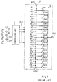
- Fig. 1 shows a typical example of the resistor string type 4-bit digital-to-analog converting unit, and comprises four input terminals IN0, IN1, IN2 and IN3 supplied with a four bit digital input signal D0, D1, D2 and D3, a controlling unit 1 coupled to the input terminals IN0 to IN3, a resistor string 2 coupled between first and second reference voltage sources REF1 and REF2, and a switching element array 3 associated with the resistor string 2.
- the resistor string 2 is implemented by resistive elements R1 to R16 coupled in series, and reference nodes N1 to N16 are provided in the resistor string 2.
- the switching element array 3 is constituted by switching elements SW1 to SW16 coupled in parallel between the reference nodes N1 to N16 and an output terminal OUT1.
- sixteen controlling signal lines CTL1 are coupled in parallel between the controlling unit 1 and the switching elements SW1 to SW16, and the switching elements SW1 to SW16 selectively conduct the associated reference nodes N1 to N16 to the output terminal OUT1.
- the controlling unit 1 is implemented by a 4-to-16 decoding circuit, and the digital input signal D0 to D3 is decoded by the controlling unit 1.
- the controlling unit 1 shifts one of the sixteen controlling signal lines CTL1 to an active level.
- the controlling signal line of the active level allows one of the switching elements SW1 to SW16 to turn on or enter a closed-state, and the voltage level at the associated reference node is propagated to the output terminal OUT1.
- Vref1 and Vref2 stand for voltage levels at the first and second reference voltage sources REF1 and REF2, and VR is indicative of the difference between the voltage levels Vref1 and Vref2.
- the resistor string 2 is constituted by 28 or 256 resistive elements.
- the prior art resistor string type digital-to-analog converting unit is integrated on a semiconductor chip, such a large number of resistive elements occupies a substantial amount of real estate on the semiconductor chip, and, accordingly, the semiconductor chip tends to be enlarged.
- resistor string type digital-to-analog converting unit is prolonged time period consumed by a testing operation.
- the uniformity of the resistor string 2 directly affects the accuracy of the digital-to-analog conversion, and the analog output signals are supplied from the reference nodes N1 to N16, respectively. Since the reference node N1 to N16 coupled to the output terminal OUT1 is moved from N1 to N16 together with increment of the binary number represented by the digital input signal. For this reason, in the testing operation, the digital input signal is incremented from zero to the maximum value, and the analog output signal is examined to see whether or not the variation is fallen within an acceptable range. This means that the examination is repeated 2 n times for n-bit digital input signal.
- the present invention proposes to selectively couple a resistive means to one of both ends of a resistor string so as to change voltage levels at reference nodes provided in the resistor string.
- a digital-to-analog converting unit comprising a) a resistor array having a series combination of a first resistive element and a plurality of second resistive elements, and a third resistive means, each of the first resistive element and the third resistive means providing a half of a resistance produced by one of the plurality of second resistive elements, the series combination having first and second ends opposite to each other, b) a plurality of first switching elements selectively shifted between open and closed states and operative to couple the third resistive means to one of the first and second ends so as to form a resistor string, the plurality of first switching elements being further operative to couple the resistor string between first and second voltage sources different in voltage level from each other, the resistor string having a plurality of reference nodes each provided between two of the first and second resistive elements, the third resistive means and the first and second voltage sources, c) a plurality of second switching elements respectively associated with the reference nodes and selectively shifted between open and
- the third resistive means may be implemented by a single resistive element, however, another implementation may alternatively use one of two resistive elements physically coupled to the first and second voltage sources.
- a resistor string type digital-to-analog converting unit embodying the present invention is fabricated on a semiconductor substrate 21, and forms a part of a large scale integration.
- the resistor string type digital-to-analog converting unit largely comprises a controlling unit 22, a resistor array 23 and an analog switching element array 24.
- the controlling unit 22 is coupled to four input nodes IN10, IN11, IN12 and IN13, and four-bit digital input signal D0, D1, D2 and D3 is supplied to the input nodes IN10 to IN13.
- the bits D0 and D3 serve as the least significant bit and the most significant bit, respectively.
- the controlling unit 22 comprises inverting circuits INV1, INV2, INV3 and INV4 for producing the complementary input signal CD0, CD1, CD2 and CD3, and eight AND gates AD1, AD2, AD3, AD4, AD5, AD6, AD7 and AD8 as shown in Fig. 3.
- Controlling lines CNL are coupled between the controlling unit 22 and the resistor array 23, and is the individual controlling signal lines are labeled with "CN1" to "CN14", respectively.
- the input node IN10 is directly coupled to the controlling lines CN1, CN4 and CN6, and the inverting circuit INV1 is coupled to the controlling signal lines CN2, CN3 and CN5. Therefore, the least significant bit D0 is transferred to the controlling signal lines CN1, CN4 and CN6, and the complementary bit thereof CD0 is supplied to the controlling signal lines CN2, CN3 and CN5.
- the input nodes IN11 to IN13 and the inverting circuits INV2 to INV4 are selectively coupled to the input nodes of the AND gates AD1 to AD8, and the output nodes of the AND gates AD1 to AD8 are respectively coupled to the controlling signal lines CN7 to CN14.
- the resistor array 23 comprises a series combination 23a of a first resistive element R11 and a plurality of second resistive elements R12, R13, R14, R15, R16, R17 and R18, and a third resistive element R19.
- Each of the second resistive elements R12 to R18 produces a unit resistance R against current
- each of the first and third resistive elements R11 and R19 provides a half of the unit resistance R against current.
- the third resistive element R19 is selectively coupled to one of both ends of the series combination 23a, and the third resistive element R19 and the series combination 23a form in combination a resistor string.
- the resistor string is constituted by seven resistive elements each producing the unit resistance R as well as two resistive elements each producing a half of the unit resistance (R/2), the total resistance of the resistor string is eight times as large as the unit resistance R, or is sixteen times as large as the half unit resistance R/2.
- the analog switching element array 24 comprises first analog switching elements SW21, SW22, SW23, SW24, SW25 and SW26 and second analog switching elements SW27, SW28, SW29, SW30, SW31, SW32, SW33 and SW34, and the first and second analog switching elements SW21 to SW34 may be implemented by transistors, respectively.
- the first analog switching elements SW21 to SW26 are gated by the controlling signal lines CN1 to CN6, respectively, and establish two current paths between first and second reference voltage sources Vref1 and Vref2 and the resistor string.
- the inverting circuit INV1 drives the controlling signal lines CN2, CN3 and CN5 to an active level, and the first analog switching elements SW22, SW23 and SW25 are concurrently shifted to closed state.
- the other first analog switching elements SW21, SW24 and SW26 are left in open-state.
- the first analog switching elements SW23 and SW25 provide a current path from the first reference voltage source Vref1 through the third resistive element R19 to the first resistive element R11, and the first analog switching element SW22 couples the second resistive element R18 to the second reference voltage source Vref2.
- the bit D0 of logic "1" level shifts the controlling signal lines CN1, CN4 and CN6 to the active level, and the first analog switching elements SW21, SW24 and SW26 establish a current path from the first reference voltage source Vref1 to the first resistive element R11 as well as a current path from the second resistive element R18 through the third resistive element R19 to the second reference voltage source Vref2.
- the other first switching elements SW22, SW23 and SW25 remain in the open state.
- the third resistive element R19 is coupled to one of the first resistive element R11 and the second resistive element R18 depending upon the bit D0 of the digital input signal, and allows reference nodes N21 to N28 to vary in voltage level by a half of the unit resistance.
- each of the reference nodes N21 to N28 can produce two different voltage levels corresponding to two binary values.
- voltage levels V21 to V28 at the respective reference nodes N21 to N28 are given as follows.
- each of the reference nodes N21 to N28 produces two different voltage levels such as V21 and V21' depending upon the logic level of the bit D0, and the alternation decreases the number of the component resistive elements R11 to R19.
- the prior art resistor string 2 needs 24 or 16 component resistive elements R1 to R16, however, the resistor string according to the present invention is constituted by nine resistive elements R11 to R19, i.e., (24 ⁇ 1 - 1) + 2. This results in reduction of real estate occupied by the resistor array 23.
- the second analog switching elements SW27 to SW34 are respectively coupled to the reference nodes N21 to N28, and selectively transfer the voltage levels V21 to V28 and V21' to V28' to an output node OUT11. Namely the second analog switching elements SW27 to SW34 are respectively gated by the controlling signal lines CN7 to CN14, and are selectively shifted between open and closed states.
- the prior art digital-to-analog converting unit shown in Fig. 1 needs sixteen switching elements SW1 to SW16
- the digital-to-analog converting unit implementing the first embodiment contains only fourteen analog switching elements SW21 to SW34, and the real estate occupied by the switching element array 24 is decreased. Thus, not only the resistor array 23 but also the switching element array 24 are decreased in size according to the present invention.
- Table 3 shows relationship between the bits D1, D2 and D3 of the digital input signal and the states of the first and second analog switching elements SW21 to SW34.
- the digital-to-analog converting characteristics are identical with one another.
- the digital-to-analog converting unit according to the present invention has various advantages over the prior art digital-to-analog converting unit.
- the occupation area of the resistor array 23 is decreased rather than that of the prior art digital-to-analog converting unit, uniformity of the resistance is easily obtained through a currently available fabrication process sequence, and the component resistive elements R11 to R19 are less affectable by crystal defects of the semiconductor substrate 21.
- the accuracy of digital-to-analog conversion is surely improved, and the production yield is enhanced in comparison with the prior art digital-to-analog converting unit.
- the testing operation is completed within a relatively short time period.
- the digital input signal D0 to D3 is sequentially incremented from zero to the maximum binary value in the testing operation on the prior art digital-to-analog converting unit.
- the prior art digital-to-analog converting unit needs 0.32 second for all of the binary values.
- the resistor string according to the present invention repeats the examination eight times for the reference nodes N21 to N28, and the testing operation is completed within 0.16 second.
- the digital-to-analog converting unit according to the present invention allows the diagnostic system to enhance the throughput, and the production cost is decreased in comparison with the prior art digital-to-analog converting unit.
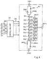
- FIG. 4 another digital-to-analog converting unit embodying the present invention is illustrated.
- the digital-to-analog converting unit shown in Fig. 4 is similar in arrangement to the first embodiment except for a third resistive means 40 and first analog switching elements SW41, SW42, SW43 and SW44. For this reason, the other component elements are designated by the same reference signs as those used in Fig. 2 without any detailed description.
- the third resistive means 40 is implemented by two resistive elements R41 and R42 each providing a half of the unit resistance (R/2), and the resistive elements R41 and R42 are coupled to the first and second reference voltage sources Vref1 and Vref2, respectively.
- the first analog switching elements SW41 and SW42 are provided in association with the first reference voltage sources Vref1. Namely, the first analog switching element SW41 is coupled between the first resistive element R11 and the first reference voltage source Vref1, and the first analog switching element SW42 is coupled between the first resistive element R11 and the resistive element R41. Since the first analog switching elements SW41 and SW42 are alternatively shifted between open and closed states, the first reference voltage source Vref1 is coupled directly to the first resistive element R11 or through the resistive element R41.
- first analog switching elements SW43 and SW44 are associated with the second reference voltage source Vref2.
- the first analog switching element SW43 is coupled between the second resistive element R18 and the second reference voltage source Vref2
- the first analog switching element SW44 is coupled to the second resistive element R18 and the resistive element R42.
- the first analog switching elements SW43 and SW44 are alternatively shifted between open and closed states, and the second resistive element R18 is coupled to the second reference voltage source Vref2 directly or through the resistive element R42.
- the first analog switching element SW43 allows the second resistive element R18 to be directly coupled to the second reference voltage source Vref2.
- the resistive element R42 participates a current path between the second resistive element R18 and the second reference voltage source Vref2.
- the third resistive means 40 selectively couples to the first and second resistive elements R11 and R18.
- the controlling unit 22 selectively shifts the first analog switching elements SW41 to SW44 depending upon the logic level of the least significant bit D0, and only one of the second analog switching elements SW27 to SW34 is shifted to the closed state depending upon the component bits D1 to D3 of the digital input signal. Therefore, a voltage level corresponding to the binary value indicated by the digital input signal D0 to D3 is supplied from one of the reference nodes N21 to N28 to the output node OUT11 as similar to the first embodiment.
- the second embodiment is further advantageous in the number of the first analog switching elements SW41 to SW44, and, accordingly, the analog output signal is less affectable by the first analog switching elements SW41 to SW44.
- a digital-to-analog converting unit according to the present invention may be fabricated on a circuit board with discrete circuit component elements.
- the first and second embodiments convert 4-bit digital input signals.
- a digital-to-analog converting unit according to the present invention may be used for a digital input signal consisting of more than 4 bits.
Landscapes
- Engineering & Computer Science (AREA)
- Theoretical Computer Science (AREA)
- Analogue/Digital Conversion (AREA)
Description
- This invention relates to a digital-to-analog converting unit and, more particularly, to a digital-to-analog converting unit of the type having a string of resistive elements (which is hereinbelow referred to as "resistor string type digital-to-analog converting unit").
- Various digital-to-analog converting units have been proposed, and resistor string type digital-to-analog converting units and resistive-ladder type digital-to-analog converting units are attractive to integrated circuits. The resistor string type digital-to-analog converting unit is implemented by a series combination of resistive elements, and an output analog voltage signal is taken out through a switching element associated with one of the nodes between two adjacent resistive elements. On the other hand, the resistive-ladder type digital-to-analog converting unit requires two kinds of resistor, i.e. a resistive R element of a unit resistance and a resistive element 2R twice as large as the resistive element R, and the resistive elements R and 2R are fabricated into a ladder-shape. The resistor string type digital-to-analog converting unit is simple in arrangement, and linearity is guaranteed on the analog output signal. Moreover, all the binary number are surely converted into corresponding analog value by the resistor string type digital-to-analog converting unit. These attractive points have found a wide variety of application.
- Fig. 1 shows a typical example of the resistor string type 4-bit digital-to-analog converting unit, and comprises four input terminals IN0, IN1, IN2 and IN3 supplied with a four bit digital input signal D0, D1, D2 and D3, a controlling
unit 1 coupled to the input terminals IN0 to IN3, aresistor string 2 coupled between first and second reference voltage sources REF1 and REF2, and aswitching element array 3 associated with theresistor string 2. Theresistor string 2 is implemented by resistive elements R1 to R16 coupled in series, and reference nodes N1 to N16 are provided in theresistor string 2. Theswitching element array 3 is constituted by switching elements SW1 to SW16 coupled in parallel between the reference nodes N1 to N16 and an output terminal OUT1. Though not shown in Fig. 1, sixteen controlling signal lines CTL1 are coupled in parallel between the controllingunit 1 and the switching elements SW1 to SW16, and the switching elements SW1 to SW16 selectively conduct the associated reference nodes N1 to N16 to the output terminal OUT1. Namely, the controllingunit 1 is implemented by a 4-to-16 decoding circuit, and the digital input signal D0 to D3 is decoded by the controllingunit 1. When the digital input signal D0 to D3 is decoded, the controllingunit 1 shifts one of the sixteen controlling signal lines CTL1 to an active level. The controlling signal line of the active level allows one of the switching elements SW1 to SW16 to turn on or enter a closed-state, and the voltage level at the associated reference node is propagated to the output terminal OUT1. The digital-to-analog converting operation is summarized in Table 1 on the assumption that the digital bits D3 and D0 serve as the most significant bit and the least significant bit, respectively, and "OP" and "CL" stand for "open-state" and "closed-state".
- Relation between the digital input signal D0 to D3 and the analog output signal is shown in Table 2. In Table 2, Vref1 and Vref2 stand for voltage levels at the first and second reference voltage sources REF1 and REF2, and VR is indicative of the difference between the voltage levels Vref1 and Vref2.
Table 2 Digital Input Signal Analog Output Signal D3 D2 D1 D0 0 0 0 0 (0/16) VR + Vref2 0 0 0 1 (1/16) VR + Vref2 0 0 1 0 (2/16) VR + Vref2 0 0 1 1 (3/16) VR + Vref2 0 1 0 0 (4/16) VR + Vref2 0 1 0 1 (5/16) VR + Vref2 0 1 1 0 (6/16) VR + Vref2 0 1 1 1 (7/16) VR + Vref2 1 0 0 0 (8/16) VR + Vref2 1 0 0 1 (9/16) VR + Vref2 1 0 1 0 (10/16) VR + Vref2 1 0 1 1 (11/16) VR + Vref2 1 1 0 0 (12/16) VR + Vref2 1 1 0 1 (13/16) VR + Vref2 1 1 1 0 (14/16) VR + Vref2 1 1 1 1 (15/16) VR + Vref2 - A problem is encountered in the prior art resistor string type digital-to-analog converting unit in that a large number of resistive elements are necessary, and the resistive elements are exponentially increased with the component bits of the digital input signal. For example, if the digital input signal consists of 8 bits, the
resistor string 2 is constituted by 2⁸ or 256 resistive elements. When the prior art resistor string type digital-to-analog converting unit is integrated on a semiconductor chip, such a large number of resistive elements occupies a substantial amount of real estate on the semiconductor chip, and, accordingly, the semiconductor chip tends to be enlarged. - The integration of such a large number of resistive elements inherently has a difficulty in the fabrication process. Namely, currently available process sequences hardly achieve uniform resistivity over the
large resistor string 2 due to fluctuation of process parameters as well as unintentional crystal defects in a resistive region. The accuracy of the digital-to-analog conversion achieved by the string resistor type digital-to-analog converting unit is directly dominated by the uniformity of the resistance of theresistor string 2, and thelarge resistor string 2 produced through one of the currently available process sequences deteriorates the accuracy of the digital-to-analog conversion. - Yet another drawback inherent in the prior art resistor string type digital-to-analog converting unit is prolonged time period consumed by a testing operation. As described hereinbefore, the uniformity of the
resistor string 2 directly affects the accuracy of the digital-to-analog conversion, and the analog output signals are supplied from the reference nodes N1 to N16, respectively. Since the reference node N1 to N16 coupled to the output terminal OUT1 is moved from N1 to N16 together with increment of the binary number represented by the digital input signal. For this reason, in the testing operation, the digital input signal is incremented from zero to the maximum value, and the analog output signal is examined to see whether or not the variation is fallen within an acceptable range. This means that the examination is repeated 2n times for n-bit digital input signal. - It is therefore an object of the present invention to provide a digital-to-analog converting unit, as defined in
claim 1, which is free from the problems inherent in the prior art resistor string type digital-to-analog converting unit. - To accomplish these object, the present invention proposes to selectively couple a resistive means to one of both ends of a resistor string so as to change voltage levels at reference nodes provided in the resistor string.
- In accordance with the present invention, there is provided a digital-to-analog converting unit comprising a) a resistor array having a series combination of a first resistive element and a plurality of second resistive elements, and a third resistive means, each of the first resistive element and the third resistive means providing a half of a resistance produced by one of the plurality of second resistive elements, the series combination having first and second ends opposite to each other, b) a plurality of first switching elements selectively shifted between open and closed states and operative to couple the third resistive means to one of the first and second ends so as to form a resistor string, the plurality of first switching elements being further operative to couple the resistor string between first and second voltage sources different in voltage level from each other, the resistor string having a plurality of reference nodes each provided between two of the first and second resistive elements, the third resistive means and the first and second voltage sources, c) a plurality of second switching elements respectively associated with the reference nodes and selectively shifted between open and closed states for coupling one of the reference nodes to an output node, and d) a controlling unit supplied with a digital input signal and selectively shifting the plurality of first switching elements and the plurality of second switching elements depending upon a binary value indicated by the digital input signal.
- The third resistive means may be implemented by a single resistive element, however, another implementation may alternatively use one of two resistive elements physically coupled to the first and second voltage sources.
- The features and advantages of the digital-to-analog converting unit according to the present invention will be more clearly understood from the following description taken in conjunction with the accompanying drawings in which:
- Fig. 1 is a circuit diagram showing the arrangement of the prior art digital-to-analog converting unit;
- Fig. 2 is a circuit diagram showing the arrangement of a resistor string type digital-to-analog converting unit according to the present invention;
- Fig. 3 is a circuit diagram showing the arrangement of a controlling unit incorporated in the resistor string type digital-to-analog converting unit shown in Fig. 2; and
- Fig. 4 is a circuit diagram showing the arrangement of another resistor string type digital-to-analog converting unit according to the present invention.
- Referring to Fig. 2 of the drawings, a resistor string type digital-to-analog converting unit embodying the present invention is fabricated on a
semiconductor substrate 21, and forms a part of a large scale integration. The resistor string type digital-to-analog converting unit largely comprises a controllingunit 22, aresistor array 23 and an analogswitching element array 24. - The controlling
unit 22 is coupled to four input nodes IN10, IN11, IN12 and IN13, and four-bit digital input signal D0, D1, D2 and D3 is supplied to the input nodes IN10 to IN13. The bits D0 and D3 serve as the least significant bit and the most significant bit, respectively. The controllingunit 22 comprises inverting circuits INV1, INV2, INV3 and INV4 for producing the complementary input signal CD0, CD1, CD2 and CD3, and eight AND gates AD1, AD2, AD3, AD4, AD5, AD6, AD7 and AD8 as shown in Fig. 3. Controlling lines CNL are coupled between the controllingunit 22 and theresistor array 23, and is the individual controlling signal lines are labeled with "CN1" to "CN14", respectively. The input node IN10 is directly coupled to the controlling lines CN1, CN4 and CN6, and the inverting circuit INV1 is coupled to the controlling signal lines CN2, CN3 and CN5. Therefore, the least significant bit D0 is transferred to the controlling signal lines CN1, CN4 and CN6, and the complementary bit thereof CD0 is supplied to the controlling signal lines CN2, CN3 and CN5. The input nodes IN11 to IN13 and the inverting circuits INV2 to INV4 are selectively coupled to the input nodes of the AND gates AD1 to AD8, and the output nodes of the AND gates AD1 to AD8 are respectively coupled to the controlling signal lines CN7 to CN14. - Turning back to Fig. 2, the
resistor array 23 comprises aseries combination 23a of a first resistive element R11 and a plurality of second resistive elements R12, R13, R14, R15, R16, R17 and R18, and a third resistive element R19. Each of the second resistive elements R12 to R18 produces a unit resistance R against current, and each of the first and third resistive elements R11 and R19 provides a half of the unit resistance R against current. As will be described hereinbelow, the third resistive element R19 is selectively coupled to one of both ends of theseries combination 23a, and the third resistive element R19 and theseries combination 23a form in combination a resistor string. Since the resistor string is constituted by seven resistive elements each producing the unit resistance R as well as two resistive elements each producing a half of the unit resistance (R/2), the total resistance of the resistor string is eight times as large as the unit resistance R, or is sixteen times as large as the half unit resistance R/2. - The analog
switching element array 24 comprises first analog switching elements SW21, SW22, SW23, SW24, SW25 and SW26 and second analog switching elements SW27, SW28, SW29, SW30, SW31, SW32, SW33 and SW34, and the first and second analog switching elements SW21 to SW34 may be implemented by transistors, respectively. The first analog switching elements SW21 to SW26 are gated by the controlling signal lines CN1 to CN6, respectively, and establish two current paths between first and second reference voltage sources Vref1 and Vref2 and the resistor string. - In detail, when the bit D0 is logic "0" level, the inverting circuit INV1 drives the controlling signal lines CN2, CN3 and CN5 to an active level, and the first analog switching elements SW22, SW23 and SW25 are concurrently shifted to closed state. The other first analog switching elements SW21, SW24 and SW26 are left in open-state. Then, the first analog switching elements SW23 and SW25 provide a current path from the first reference voltage source Vref1 through the third resistive element R19 to the first resistive element R11, and the first analog switching element SW22 couples the second resistive element R18 to the second reference voltage source Vref2.
- On the other hand, the bit D0 of logic "1" level shifts the controlling signal lines CN1, CN4 and CN6 to the active level, and the first analog switching elements SW21, SW24 and SW26 establish a current path from the first reference voltage source Vref1 to the first resistive element R11 as well as a current path from the second resistive element R18 through the third resistive element R19 to the second reference voltage source Vref2. However, the other first switching elements SW22, SW23 and SW25 remain in the open state. Thus, the third resistive element R19 is coupled to one of the first resistive element R11 and the second resistive element R18 depending upon the bit D0 of the digital input signal, and allows reference nodes N21 to N28 to vary in voltage level by a half of the unit resistance. In other words, each of the reference nodes N21 to N28 can produce two different voltage levels corresponding to two binary values. In a case where the bit D0 is logic "0" level, voltage levels V21 to V28 at the respective reference nodes N21 to N28 are given as follows.





art resistor string 2 needs 2⁴ or 16 component resistive elements R1 to R16, however, the resistor string according to the present invention is constituted by nine resistive elements R11 to R19, i.e., (2⁴⁻¹ - 1) + 2. This results in reduction of real estate occupied by theresistor array 23. - The second analog switching elements SW27 to SW34 are respectively coupled to the reference nodes N21 to N28, and selectively transfer the voltage levels V21 to V28 and V21' to V28' to an output node OUT11. Namely the second analog switching elements SW27 to SW34 are respectively gated by the controlling signal lines CN7 to CN14, and are selectively shifted between open and closed states. Although the prior art digital-to-analog converting unit shown in Fig. 1 needs sixteen switching elements SW1 to SW16, the digital-to-analog converting unit implementing the first embodiment contains only fourteen analog switching elements SW21 to SW34, and the real estate occupied by the switching
element array 24 is decreased. Thus, not only theresistor array 23 but also theswitching element array 24 are decreased in size according to the present invention. - Table 3 shows relationship between the bits D1, D2 and D3 of the digital input signal and the states of the first and second analog switching elements SW21 to SW34.

- The relation between the digital input signal D0 to D3 and the analog output signal is summarized in Table 4.
Table 4 Digital Input Signal Analog Output Signal D3 D2 D1 D0 0 0 0 0 (0/16) VR + Vref2 0 0 0 1 (1/16) VR + Vref2 0 0 1 0 (2/16) VR + Vref2 0 0 1 1 (3/16) VR + Vref2 0 1 0 0 (4/16) VR + Vref2 0 1 0 1 (5/16) VR + Vref2 0 1 1 0 (6/16) VR + Vref2 0 1 1 1 (7/16) VR + Vref2 1 0 0 0 (8/16) VR + Vref2 1 0 0 1 (9/16) VR + Vref2 1 0 1 0 (10/16) VR + Vref2 1 0 1 1 (11/16) VR + Vref2 1 1 0 0 (12/16) VR + Vref2 1 1 0 1 (13/16) VR + Vref2 1 1 1 0 (14/16) VR + Vref2 1 1 1 1 (15/16) VR + Vref2 - Comparing Table 4 with Table 2, the digital-to-analog converting characteristics are identical with one another. However, the digital-to-analog converting unit according to the present invention has various advantages over the prior art digital-to-analog converting unit. First, since the occupation area of the
resistor array 23 is decreased rather than that of the prior art digital-to-analog converting unit, uniformity of the resistance is easily obtained through a currently available fabrication process sequence, and the component resistive elements R11 to R19 are less affectable by crystal defects of thesemiconductor substrate 21. As a result, the accuracy of digital-to-analog conversion is surely improved, and the production yield is enhanced in comparison with the prior art digital-to-analog converting unit. - Second, the testing operation is completed within a relatively short time period. The digital input signal D0 to D3 is sequentially incremented from zero to the maximum binary value in the testing operation on the prior art digital-to-analog converting unit. Assuming now that the single examination for a binary value consumes 0.02 second, the prior art digital-to-analog converting unit needs 0.32 second for all of the binary values. However, the resistor string according to the present invention repeats the examination eight times for the reference nodes N21 to N28, and the testing operation is completed within 0.16 second. Thus, the digital-to-analog converting unit according to the present invention allows the diagnostic system to enhance the throughput, and the production cost is decreased in comparison with the prior art digital-to-analog converting unit.
- Turning to Fig. 4, another digital-to-analog converting unit embodying the present invention is illustrated. The digital-to-analog converting unit shown in Fig. 4 is similar in arrangement to the first embodiment except for a third resistive means 40 and first analog switching elements SW41, SW42, SW43 and SW44. For this reason, the other component elements are designated by the same reference signs as those used in Fig. 2 without any detailed description.
- The third resistive means 40 is implemented by two resistive elements R41 and R42 each providing a half of the unit resistance (R/2), and the resistive elements R41 and R42 are coupled to the first and second reference voltage sources Vref1 and Vref2, respectively. The first analog switching elements SW41 and SW42 are provided in association with the first reference voltage sources Vref1. Namely, the first analog switching element SW41 is coupled between the first resistive element R11 and the first reference voltage source Vref1, and the first analog switching element SW42 is coupled between the first resistive element R11 and the resistive element R41. Since the first analog switching elements SW41 and SW42 are alternatively shifted between open and closed states, the first reference voltage source Vref1 is coupled directly to the first resistive element R11 or through the resistive element R41.
- Similarly, the first analog switching elements SW43 and SW44 are associated with the second reference voltage source Vref2. The first analog switching element SW43 is coupled between the second resistive element R18 and the second reference voltage source Vref2, and the first analog switching element SW44 is coupled to the second resistive element R18 and the resistive element R42. The first analog switching elements SW43 and SW44 are alternatively shifted between open and closed states, and the second resistive element R18 is coupled to the second reference voltage source Vref2 directly or through the resistive element R42.
- When the resistive element R41 is coupled to the first resistive element R11, the first analog switching element SW43 allows the second resistive element R18 to be directly coupled to the second reference voltage source Vref2. On the other hand, while the first analog switching element SW41 directly couples the first reference voltage source Vref1 to the first resistive element R11, the resistive element R42 participates a current path between the second resistive element R18 and the second reference voltage source Vref2. Thus, only one of the resistive elements R41 and R42 forms a part of a current path between the first and second reference voltage sources Vref1 and Vref2, and, for this reason, the third resistive means 40 selectively couples to the first and second resistive elements R11 and R18.
- In operation, the controlling
unit 22 selectively shifts the first analog switching elements SW41 to SW44 depending upon the logic level of the least significant bit D0, and only one of the second analog switching elements SW27 to SW34 is shifted to the closed state depending upon the component bits D1 to D3 of the digital input signal. Therefore, a voltage level corresponding to the binary value indicated by the digital input signal D0 to D3 is supplied from one of the reference nodes N21 to N28 to the output node OUT11 as similar to the first embodiment. - All of the advantages described hereinbefore are achieved by the digital-to-analog converting unit implementing the second embodiment. The second embodiment is further advantageous in the number of the first analog switching elements SW41 to SW44, and, accordingly, the analog output signal is less affectable by the first analog switching elements SW41 to SW44.
- Although particular embodiments of the present invention have been shown and described, it will be obvious to those skilled in the art that various changes and modifications may be made without departing from the spirit and scope of the present invention. For example, a digital-to-analog converting unit according to the present invention may be fabricated on a circuit board with discrete circuit component elements. The first and second embodiments convert 4-bit digital input signals. However, a digital-to-analog converting unit according to the present invention may be used for a digital input signal consisting of more than 4 bits.
Claims (3)
- A digital-to-analog converting unit comprisinga) a series combination of a first resistive element (R11) and second resistive elements (R12 to R18) and operative to allow a current to flow from a first voltage source (Vref1) to a second voltage source (Vref2),b) a plurality of switching elements (SW27 to SW34) associated with said series combination and selectively shifted between open and closed states for transferring an analog output signal to an output node (OUT11), andc) a controlling unit (22) supplied with a digital input signal (D0 to D3) and selectively shifting said switching elements,characterized byd) a third resistive means (R19; R41/R42), each of said first resistive element and said third resistive means providing a half of a resistance produced by one of said second resistive elements, ande) other switching elements (SW21 to SW26; SW41 to SW44) selectively shifted between open and closed states and selectively coupling said third resistive means to one of first and second ends of said series combination so as to form a resistor string, said other switching elements further being operative to couple said resistor string between said first and second voltage sources, said resistor string having a plurality of reference nodes (N21 to N28) respectively coupled to said switching elements, each of said reference nodes being provided between two of said first and second resistive elements, said third resistive means and said first and second voltage sources,and in that
said controlling unit selectively shifts said switching elements and said other switching elements depending upon a binary value indicated by said digital input signal. - A digital-to-analog converting unit as set forth in claim 1, in which said third resistive means is formed by a single resistive element (R19), and in which said first switching elements selectively couple the single resistive element between said first voltage source and said first end and between said second end and said second voltage source, said one of said first switching elements (SW22) coupling said second end to said second voltage source while said single resistive element is coupled between said first voltage source and said first end, another first switching element (SW21) alternatively coupling said first voltage source to said first end while said single resistive element is coupled between said second end and said second voltage source.
- A digital-to-analog converting unit as set forth in claim 1, in which said third resistive means is implemented by two resistive elements (R41/R42) coupled to said first and second voltage sources, respectively, each of said resistive elements providing a half of said resistance, and in which said first analog switching elements alternatively provides a current path from said first voltage source through one of said resistive elements (R41) coupled to said first voltage source and said series combination to said second voltage source and a current path from said first voltage source through said series combination and the other of said resistive elements (R42) coupled to said second voltage source to said second voltage source.
Applications Claiming Priority (2)
| Application Number | Priority Date | Filing Date | Title |
|---|---|---|---|
| JP02203312A JP3130528B2 (en) | 1990-07-31 | 1990-07-31 | Digital to analog converter |
| JP203312/90 | 1990-07-31 |
Publications (3)
| Publication Number | Publication Date |
|---|---|
| EP0469556A2 EP0469556A2 (en) | 1992-02-05 |
| EP0469556A3 EP0469556A3 (en) | 1993-08-11 |
| EP0469556B1 true EP0469556B1 (en) | 1996-05-15 |
Family
ID=16471944
Family Applications (1)
| Application Number | Title | Priority Date | Filing Date |
|---|---|---|---|
| EP91112809A Expired - Lifetime EP0469556B1 (en) | 1990-07-31 | 1991-07-30 | Digital-to-analog converting unit equipped with resistor string variable in resistances at reference nodes |
Country Status (4)
| Country | Link |
|---|---|
| US (1) | US5126740A (en) |
| EP (1) | EP0469556B1 (en) |
| JP (1) | JP3130528B2 (en) |
| DE (1) | DE69119504T2 (en) |
Families Citing this family (24)
| Publication number | Priority date | Publication date | Assignee | Title |
|---|---|---|---|---|
| DE69222893T2 (en) * | 1991-06-18 | 1998-03-05 | Fujitsu Ltd | Digital-to-analog converter with resistor networks |
| US5371500A (en) * | 1992-09-11 | 1994-12-06 | Delco Electronics Corporation | Maintaining ratiometric data in electronically manipulated signal processing systems |
| JPH06224642A (en) * | 1993-01-28 | 1994-08-12 | Sanyo Electric Co Ltd | Frequency adjustment circuit for fm modulator |
| JPH06311039A (en) * | 1993-04-21 | 1994-11-04 | Nippon Philips Kk | Digital-analog converter |
| US5424740A (en) * | 1993-08-11 | 1995-06-13 | Holtek Microelectronics Inc. | Digital-to-analog converter with a Johnson code generator |
| US5467036A (en) * | 1993-09-01 | 1995-11-14 | Rohm Co., Ltd. | Integrated circuit device for driving elements and light emitting device |
| JPH07170188A (en) * | 1993-12-14 | 1995-07-04 | Yamaha Corp | D/a converter circuit |
| JP3439515B2 (en) * | 1993-12-28 | 2003-08-25 | 富士通株式会社 | Digital / analog converter |
| USRE38083E1 (en) | 1994-03-18 | 2003-04-22 | Analog Devices, Inc. | Rail-to-rail DAC drive circuit |
| US5617091A (en) * | 1994-09-02 | 1997-04-01 | Lowe, Price, Leblanc & Becker | Resistance ladder, D-A converter, and A-D converter |
| US5831566A (en) * | 1996-05-07 | 1998-11-03 | Vlsi Technology, Inc. | Low voltage digital-to-analog converter |
| US5703588A (en) * | 1996-10-15 | 1997-12-30 | Atmel Corporation | Digital to analog converter with dual resistor string |
| US5808576A (en) * | 1997-02-24 | 1998-09-15 | Texas Instruments Incorporated | Resistor string digital-to-analog converter |
| US6163289A (en) * | 1997-09-23 | 2000-12-19 | Philips Electronics North America Corp. | Differential voltage digital-to-analog converter |
| US6573811B2 (en) * | 2001-02-07 | 2003-06-03 | National Semiconductor Corporation | Resistor tuning network and method for microelectronic RC-based filters |
| US6876590B2 (en) * | 2002-11-20 | 2005-04-05 | Infineon Technologies, Ag | 2T2C signal margin test mode using a defined charge exchange between BL and/BL |
| US6826099B2 (en) * | 2002-11-20 | 2004-11-30 | Infineon Technologies Ag | 2T2C signal margin test mode using a defined charge and discharge of BL and /BL |
| US6731554B1 (en) * | 2002-11-20 | 2004-05-04 | Infineon Technologies Ag | 2T2C signal margin test mode using resistive element |
| US20040095799A1 (en) * | 2002-11-20 | 2004-05-20 | Michael Jacob | 2T2C signal margin test mode using different pre-charge levels for BL and/BL |
| US6778122B2 (en) * | 2002-12-23 | 2004-08-17 | Institute Of Microelectronics | Resistor string digital to analog converter with differential outputs and reduced switch count |
| JP2004212668A (en) * | 2002-12-27 | 2004-07-29 | Koninkl Philips Electronics Nv | Gradation voltage output apparatus |
| US6937178B1 (en) | 2003-05-15 | 2005-08-30 | Linear Technology Corporation | Gradient insensitive split-core digital to analog converter |
| US8004439B2 (en) * | 2009-11-30 | 2011-08-23 | Himax Technologies Limited | Digital to analog converter |
| US9444487B1 (en) * | 2015-08-27 | 2016-09-13 | Analog Devices Global | Multiple stage digital to analog converter |
Family Cites Families (12)
| Publication number | Priority date | Publication date | Assignee | Title |
|---|---|---|---|---|
| US3918046A (en) * | 1973-02-22 | 1975-11-04 | Xerox Corp | Digital to analog converter |
| DE2445142C3 (en) * | 1974-09-20 | 1980-10-16 | Siemens Ag, 1000 Berlin Und 8000 Muenchen | Analog-to-digital converters and digital-to-analog converters and procedures for their operation |
| JPS5441061A (en) * | 1977-09-08 | 1979-03-31 | Sony Corp | Analogue/digital converter |
| GB1600853A (en) * | 1977-09-29 | 1981-10-21 | Solartron Electronic Group | Analogue to digital converters |
| US4468607A (en) * | 1981-05-07 | 1984-08-28 | Sanyo Electric Co., Ltd. | Ladder-type signal attenuator |
| US4742329A (en) * | 1985-01-28 | 1988-05-03 | Sanyo Electric Co., Ltd. | Digital/analog converter |
| JPS62200915A (en) * | 1986-02-28 | 1987-09-04 | Nec Ic Microcomput Syst Ltd | Reference voltage generation circuit |
| JPH0732364B2 (en) * | 1986-03-28 | 1995-04-10 | 富士通株式会社 | Digital-to-analog converter |
| US4837572A (en) * | 1987-07-20 | 1989-06-06 | Zdzislaw Gulczynski | Digital-to-analog converter |
| US4924225A (en) * | 1988-01-28 | 1990-05-08 | Harris Semiconductor Patents, Inc. | Analog to digital converter with integral linearity error compensation and method of operation |
| US4908623A (en) * | 1988-08-08 | 1990-03-13 | Honeywell Inc. | Apparatus and method for range control and supply voltage compensation in a dual slope analog to digital converter |
| US4896157A (en) * | 1989-01-17 | 1990-01-23 | Motorola, Inc. | Digital to analog converter having single resistive string with shiftable voltage thereacross |
-
1990
- 1990-07-31 JP JP02203312A patent/JP3130528B2/en not_active Expired - Fee Related
-
1991
- 1991-07-22 US US07/734,235 patent/US5126740A/en not_active Expired - Fee Related
- 1991-07-30 DE DE69119504T patent/DE69119504T2/en not_active Expired - Fee Related
- 1991-07-30 EP EP91112809A patent/EP0469556B1/en not_active Expired - Lifetime
Also Published As
| Publication number | Publication date |
|---|---|
| JPH0488724A (en) | 1992-03-23 |
| EP0469556A2 (en) | 1992-02-05 |
| EP0469556A3 (en) | 1993-08-11 |
| DE69119504D1 (en) | 1996-06-20 |
| DE69119504T2 (en) | 1997-01-02 |
| JP3130528B2 (en) | 2001-01-31 |
| US5126740A (en) | 1992-06-30 |
Similar Documents
| Publication | Publication Date | Title |
|---|---|---|
| US5126740A (en) | Digital-to-analog converting unit equipped with resistor string variable in resistances at reference nodes | |
| US5495245A (en) | Digital-to-analog converter with segmented resistor string | |
| CN101588181B (en) | Digital-to-analog converting circuit, data driver and display device | |
| US5696508A (en) | Comparator-offset compensating converter | |
| EP0102609B1 (en) | Digital-analog converter | |
| US8963757B2 (en) | D/A converter including higher-order resistor string | |
| JPH08237128A (en) | Digital-to-analog converter with reduced number of resistors | |
| JPH01158823A (en) | Digital-analog converter with switching function compensation | |
| JPH0964744A (en) | Digital-to-analog conversion circuit | |
| US5212482A (en) | Digital-to-analog converter having an externally selectable output voltage range | |
| US7375670B1 (en) | Digital-to-analog converter | |
| JPH0377430A (en) | D/a converter | |
| US5175548A (en) | Digital-analog converter including a reduced number of resistors arranged in a string | |
| US5065159A (en) | Digital to analog converter with switching logic minimization | |
| KR20040099887A (en) | 10 bit digital/analog converter with new deglitch circuit and new 2-dimensionally hierarchical symmetric centroid switching order | |
| JP2585395B2 (en) | Impedance conversion circuit for multi-bit digital word signal in separated transmission line | |
| JP3723362B2 (en) | Flash analog / digital converter | |
| CN119652319B (en) | A digital-to-analog conversion circuit, a digital-to-analog converter, and an electronic device. | |
| JPH0846515A (en) | D/a converter | |
| JP4330232B2 (en) | Current mode D / A converter | |
| EP1608074A1 (en) | Digital-analog converter circuit | |
| CN115514371A (en) | A R-2R Digital-to-Analog Converter | |
| KR100278991B1 (en) | Linear / Nonlinear Digital to Analog Converters | |
| CN118921059A (en) | Voltage division nested resistance type digital-to-analog converter | |
| JPH1174792A (en) | Digital-to-analog conversion circuit |
Legal Events
| Date | Code | Title | Description |
|---|---|---|---|
| PUAI | Public reference made under article 153(3) epc to a published international application that has entered the european phase |
Free format text: ORIGINAL CODE: 0009012 |
|
| 17P | Request for examination filed |
Effective date: 19910730 |
|
| AK | Designated contracting states |
Kind code of ref document: A2 Designated state(s): DE FR GB |
|
| PUAL | Search report despatched |
Free format text: ORIGINAL CODE: 0009013 |
|
| AK | Designated contracting states |
Kind code of ref document: A3 Designated state(s): DE FR GB |
|
| 17Q | First examination report despatched |
Effective date: 19950706 |
|
| GRAH | Despatch of communication of intention to grant a patent |
Free format text: ORIGINAL CODE: EPIDOS IGRA |
|
| GRAA | (expected) grant |
Free format text: ORIGINAL CODE: 0009210 |
|
| AK | Designated contracting states |
Kind code of ref document: B1 Designated state(s): DE FR GB |
|
| REF | Corresponds to: |
Ref document number: 69119504 Country of ref document: DE Date of ref document: 19960620 |
|
| ET | Fr: translation filed | ||
| PLBE | No opposition filed within time limit |
Free format text: ORIGINAL CODE: 0009261 |
|
| STAA | Information on the status of an ep patent application or granted ep patent |
Free format text: STATUS: NO OPPOSITION FILED WITHIN TIME LIMIT |
|
| 26N | No opposition filed | ||
| PGFP | Annual fee paid to national office [announced via postgrant information from national office to epo] |
Ref country code: FR Payment date: 20000711 Year of fee payment: 10 |
|
| PGFP | Annual fee paid to national office [announced via postgrant information from national office to epo] |
Ref country code: GB Payment date: 20000726 Year of fee payment: 10 |
|
| PGFP | Annual fee paid to national office [announced via postgrant information from national office to epo] |
Ref country code: DE Payment date: 20000729 Year of fee payment: 10 |
|
| PG25 | Lapsed in a contracting state [announced via postgrant information from national office to epo] |
Ref country code: GB Free format text: LAPSE BECAUSE OF NON-PAYMENT OF DUE FEES Effective date: 20010730 |
|
| GBPC | Gb: european patent ceased through non-payment of renewal fee |
Effective date: 20010730 |
|
| PG25 | Lapsed in a contracting state [announced via postgrant information from national office to epo] |
Ref country code: FR Free format text: LAPSE BECAUSE OF NON-PAYMENT OF DUE FEES Effective date: 20020329 |
|
| PG25 | Lapsed in a contracting state [announced via postgrant information from national office to epo] |
Ref country code: DE Free format text: LAPSE BECAUSE OF NON-PAYMENT OF DUE FEES Effective date: 20020501 |
|
| REG | Reference to a national code |
Ref country code: FR Ref legal event code: ST |