EP0469552B1 - Optical pickup device - Google Patents
Optical pickup device Download PDFInfo
- Publication number
- EP0469552B1 EP0469552B1 EP91112802A EP91112802A EP0469552B1 EP 0469552 B1 EP0469552 B1 EP 0469552B1 EP 91112802 A EP91112802 A EP 91112802A EP 91112802 A EP91112802 A EP 91112802A EP 0469552 B1 EP0469552 B1 EP 0469552B1
- Authority
- EP
- European Patent Office
- Prior art keywords
- light
- optical
- reflection
- focusing
- recording medium
- Prior art date
- Legal status (The legal status is an assumption and is not a legal conclusion. Google has not performed a legal analysis and makes no representation as to the accuracy of the status listed.)
- Expired - Lifetime
Links
- 230000003287 optical effect Effects 0.000 title claims abstract description 121
- 230000010287 polarization Effects 0.000 claims abstract description 35
- 239000002131 composite material Substances 0.000 claims abstract description 24
- 239000004065 semiconductor Substances 0.000 abstract description 20
- 239000000758 substrate Substances 0.000 abstract description 6
- 238000005192 partition Methods 0.000 abstract description 4
- 238000001514 detection method Methods 0.000 abstract description 3
- 238000000034 method Methods 0.000 abstract description 3
- 238000004513 sizing Methods 0.000 abstract description 2
- 238000010586 diagram Methods 0.000 description 11
- 239000000470 constituent Substances 0.000 description 4
- 238000005516 engineering process Methods 0.000 description 4
- 238000000926 separation method Methods 0.000 description 4
- 230000008878 coupling Effects 0.000 description 3
- 238000010168 coupling process Methods 0.000 description 3
- 238000005859 coupling reaction Methods 0.000 description 3
- 230000005284 excitation Effects 0.000 description 3
- VYPSYNLAJGMNEJ-UHFFFAOYSA-N Silicium dioxide Chemical compound O=[Si]=O VYPSYNLAJGMNEJ-UHFFFAOYSA-N 0.000 description 2
- 230000005540 biological transmission Effects 0.000 description 2
- 230000008859 change Effects 0.000 description 2
- 238000006243 chemical reaction Methods 0.000 description 2
- 238000004891 communication Methods 0.000 description 2
- 239000011521 glass Substances 0.000 description 2
- 230000010354 integration Effects 0.000 description 2
- XUIMIQQOPSSXEZ-UHFFFAOYSA-N Silicon Chemical compound [Si] XUIMIQQOPSSXEZ-UHFFFAOYSA-N 0.000 description 1
- 230000004075 alteration Effects 0.000 description 1
- 229910052681 coesite Inorganic materials 0.000 description 1
- 238000010276 construction Methods 0.000 description 1
- 229910052906 cristobalite Inorganic materials 0.000 description 1
- 230000003247 decreasing effect Effects 0.000 description 1
- 230000006866 deterioration Effects 0.000 description 1
- 230000005684 electric field Effects 0.000 description 1
- 238000000609 electron-beam lithography Methods 0.000 description 1
- 230000002349 favourable effect Effects 0.000 description 1
- 239000012467 final product Substances 0.000 description 1
- 230000007274 generation of a signal involved in cell-cell signaling Effects 0.000 description 1
- 230000012447 hatching Effects 0.000 description 1
- 239000000463 material Substances 0.000 description 1
- 238000012986 modification Methods 0.000 description 1
- 230000004048 modification Effects 0.000 description 1
- 238000000059 patterning Methods 0.000 description 1
- 238000001020 plasma etching Methods 0.000 description 1
- 238000011160 research Methods 0.000 description 1
- 229910052710 silicon Inorganic materials 0.000 description 1
- 239000010703 silicon Substances 0.000 description 1
- 239000000377 silicon dioxide Substances 0.000 description 1
- 229910052682 stishovite Inorganic materials 0.000 description 1
- 229910052905 tridymite Inorganic materials 0.000 description 1
Images


Classifications
-
- G—PHYSICS
- G11—INFORMATION STORAGE
- G11B—INFORMATION STORAGE BASED ON RELATIVE MOVEMENT BETWEEN RECORD CARRIER AND TRANSDUCER
- G11B7/00—Recording or reproducing by optical means, e.g. recording using a thermal beam of optical radiation by modifying optical properties or the physical structure, reproducing using an optical beam at lower power by sensing optical properties; Record carriers therefor
- G11B7/12—Heads, e.g. forming of the optical beam spot or modulation of the optical beam
- G11B7/135—Means for guiding the beam from the source to the record carrier or from the record carrier to the detector
- G11B7/1356—Double or multiple prisms, i.e. having two or more prisms in cooperation
-
- G—PHYSICS
- G11—INFORMATION STORAGE
- G11B—INFORMATION STORAGE BASED ON RELATIVE MOVEMENT BETWEEN RECORD CARRIER AND TRANSDUCER
- G11B11/00—Recording on or reproducing from the same record carrier wherein for these two operations the methods are covered by different main groups of groups G11B3/00 - G11B7/00 or by different subgroups of group G11B9/00; Record carriers therefor
- G11B11/10—Recording on or reproducing from the same record carrier wherein for these two operations the methods are covered by different main groups of groups G11B3/00 - G11B7/00 or by different subgroups of group G11B9/00; Record carriers therefor using recording by magnetic means or other means for magnetisation or demagnetisation of a record carrier, e.g. light induced spin magnetisation; Demagnetisation by thermal or stress means in the presence or not of an orienting magnetic field
- G11B11/105—Recording on or reproducing from the same record carrier wherein for these two operations the methods are covered by different main groups of groups G11B3/00 - G11B7/00 or by different subgroups of group G11B9/00; Record carriers therefor using recording by magnetic means or other means for magnetisation or demagnetisation of a record carrier, e.g. light induced spin magnetisation; Demagnetisation by thermal or stress means in the presence or not of an orienting magnetic field using a beam of light or a magnetic field for recording by change of magnetisation and a beam of light for reproducing, i.e. magneto-optical, e.g. light-induced thermomagnetic recording, spin magnetisation recording, Kerr or Faraday effect reproducing
- G11B11/10532—Heads
- G11B11/10541—Heads for reproducing
- G11B11/10543—Heads for reproducing using optical beam of radiation
-
- G—PHYSICS
- G11—INFORMATION STORAGE
- G11B—INFORMATION STORAGE BASED ON RELATIVE MOVEMENT BETWEEN RECORD CARRIER AND TRANSDUCER
- G11B7/00—Recording or reproducing by optical means, e.g. recording using a thermal beam of optical radiation by modifying optical properties or the physical structure, reproducing using an optical beam at lower power by sensing optical properties; Record carriers therefor
- G11B7/12—Heads, e.g. forming of the optical beam spot or modulation of the optical beam
- G11B7/123—Integrated head arrangements, e.g. with source and detectors mounted on the same substrate
- G11B7/124—Integrated head arrangements, e.g. with source and detectors mounted on the same substrate the integrated head arrangements including waveguides
-
- G—PHYSICS
- G11—INFORMATION STORAGE
- G11B—INFORMATION STORAGE BASED ON RELATIVE MOVEMENT BETWEEN RECORD CARRIER AND TRANSDUCER
- G11B7/00—Recording or reproducing by optical means, e.g. recording using a thermal beam of optical radiation by modifying optical properties or the physical structure, reproducing using an optical beam at lower power by sensing optical properties; Record carriers therefor
- G11B7/12—Heads, e.g. forming of the optical beam spot or modulation of the optical beam
- G11B7/135—Means for guiding the beam from the source to the record carrier or from the record carrier to the detector
- G11B7/1353—Diffractive elements, e.g. holograms or gratings
-
- G—PHYSICS
- G11—INFORMATION STORAGE
- G11B—INFORMATION STORAGE BASED ON RELATIVE MOVEMENT BETWEEN RECORD CARRIER AND TRANSDUCER
- G11B7/00—Recording or reproducing by optical means, e.g. recording using a thermal beam of optical radiation by modifying optical properties or the physical structure, reproducing using an optical beam at lower power by sensing optical properties; Record carriers therefor
- G11B7/12—Heads, e.g. forming of the optical beam spot or modulation of the optical beam
- G11B7/135—Means for guiding the beam from the source to the record carrier or from the record carrier to the detector
- G11B7/1359—Single prisms
Definitions
- the present invention relates to an optical device for extracting information represented by polarized light coming from an optical object, such as an optical recording medium.
- the optical recording medium includes in addition to an optical recording medium such as an optical disk or an optical card, a magnetooptical recording medium such as a magnetooptical disk or a magnetooptical card.
- the optical pickup device according to the present invention may naturally be used not only to read data from the optical recording medium but also to write data thereon.
- an optical pickup device includes constituent elements such as a first optical system for collimating light irradiated from a semiconductor laser, a second optical system for focusing the collimated light onto an optical recording medium and for collimating light reflected from the optical recording medium, a first polarization beam splitter for separating through polarization the reflection light thus collimated by the second optical system, a second polarization beam splitter for separating the light from the first polarization beam splitter into tracking control light and focusing control light, a third optical system for focusing the separated tracking control light onto a light receiving surface of a tracking control photosensor, a fourth optical system for focusing the separated focusing control light onto a light receiving surface of a focusing control photosensor, and a fifth optical system disposed in the third or fourth optical system for guiding light to a photosensor producing a readout signal.
- constituent elements such as a first optical system for collimating light irradiated from a semiconductor laser, a second optical system for focusing the collimated light onto an optical
- the conventional optical pickup device of this type is ordinarily constituted with a large number of optical parts and hence is heavy, which leads to a problem of a slow access time.
- the cost thereof is increased and assemblage and adjustment of these parts take a great amount of human labor and a long period of time, which also leads to the problem that the cost of the final product is increased.
- a light reflected from a magnetooptical disk is guided by the focusing grating couplers into the waveguide layer; moreover, the light is separated to be converged depending on the modes.
- the resultant reflection light is sensed so as to produce a tracking error signal, a focusing error signal, and an information readout signal.
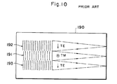
- Fig. 10 shows the focusing grating couplers described in the article above.
- three focusing grating couplers 191, 192, and 193 are fabricated side by side on a waveguide layer formed on a substrate 190.
- the reflection light from the magnetooptical disk is irradiated onto the focusing grating couplers 191 to 193 from a position thereabove with a right incident angle or an oblique incident angle.
- These focusing grating couplers are manfactured such that the coupler 191 has a grating period slightly larger than those of the couplers 192 and 193 so as to excite a light in the TM mode and the couplers 192 and 193 excite a light in the TE mode.
- the light reflected from the magnetooptical disk is represented as a composite vector including a P component (Ep) and an S component (Es) of the electric field.
- Ep P component
- Es S component
- the Ep component of the reflection light satisfies the phase matching condition in the focusing grating coupler 191, which leads to an excitation of the TM mode light.
- the phase matching condition holds in the focusing grating couplers 192 and 193, which hence cause an excitation of the TE mode light.
- the Ep component a light coupling rarely takes place in the grating couplers 192 and 193; whereas, for the Es component, the optical coupling hardly occurs in the coupler 191.
- the Ep and Es components of the light reflected from the magnetooptical disk are separated through the coupler 191 and the couplers 192 and 193, respectively so as to be focused on the respective focal points (on a wavefguide layer or on an end surface of the substrate 190).
- Each focused light is received by a photosensor associated therewith. Based on signals produced from the photosensors related to that light, the system creates a readout signal, a focusing error signal, and a tracking error signal.
- the two kinds of waveguide modes namely, the TM and TE modes are excited only in the respective separated regions. More specifically, the light in the TM and TE modes is excited only in the region of the coupler 191 and in the area of the couplers 192 and 193, respectively. This leads to a problem of deterioration of the light utilization efficiency.
- the light reflected from the magnetooptical disk is illuminated onto the entire region of the focusing grating couplers 191 to 193, the optical coupling of the light with the waveguide layer takes place only in some portions of the region. Consequently the quantity of the reflection light incident to the photosensors is decreased and hence it is difficult to detect various kinds of signals in a stable condition.
- a compact light-weight pickup device for an optical disk similarly employing the optical integration technology.
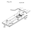
- Such a pickup device has been described, for example, in an article "An Integrated-Optic Disk Pickup Device", S. Ura et al., Institute of Electronics, Information, and Communication Engineers of Japan, Quantum Electronics Study Group 0QE85-72.
- Fig. 11 shows a portion of the optical pickup device.
- a waveguide layer 202 is formed with a glass material.
- a focusing grating coupler 203 and a waveguide beam splitter (grating) 204 are manufactured in a chirped structure by use of a patterning technology based on an electron beam lithography and a reactive ion etching technology.
- a laser diode 205 disposed on an end surface of the substrate 200 emits light, which propagates through the waveguide layer 202 to be irradiated to an upward direction by the focusing grating coupler 203 so as to be focused onto a surface of an optical disk 209.
- the waveguide beam splitter 204 develops three functions including a separation of a wave surface or wavefront, deflection of an incident light, and focusing or converging the light.
- the light radiated from the laser diode 205 passes twice through the waveguide beam splitter 204 and the focusing grating coupler 203 before the light is received by the photoelectric converter 206, namely, the light passes these units each time the light proceeds in a direction from the laser diode 205 to the optical disk 209 and in a direction from the disk 209 to the photoelectric conversion element 206. Consequently, the light passes a grating structure four times before the light is sensed. Namely, the light received by the photoelectric converter 206 becomes to be considerably weak and hence a signal produced therefrom has a minimized intensity.
- An optical device according to the preamble of claim 1 is known from JP-A-61 003 330.
- an optical device as defined in claim 1.
- Fig. 1 and Figs. 2a and 2b show a schematic diagram showing an optical pickup device, that is the constitution of an optical pickup head used to record information on and to read information a magnetooptical disk.
- the optical head includes a semiconductor laser 131 and a focusing optical system for converging onto a surface of a magnetooptical disk 134 divergent light emitted from the laser 131.
- the optical system comprises a collimation lens 132 for collimating the emitted light and an objective 133 for converging the collimated light.
- a composite beam splitter 135 is disposed in an optical path of the divergent light between the semiconductor laser 131 and tne collimation lens 132.
- the composite beam splitter 135 has two reflection surfaces 136 and 137, which are arranged to be orthogonal to each other. Each of the reflection surfaces is inclined by 45° with respect to an optical axis of the focusing optical system.
- the compsite beam splitter 135 may be constituted with four dielectric blocks (e.g. glass prisms). Each of the blocks includes surfaces respectively coated with reflection films so as to develop functions respectively of the reflection surfaces 136 and 137. The combined four dielectric blocks are bonded to each other.
- the reflection surfaces 136 and 137 are configured so as to pass therethrough to a possible extent the emission light from the semiconductor laser 131 and to refiect a portion (for example, 10%) of a light reflected from the magnetooptical disk 134. In this regard, the optical reflection efficiency of each of the reflection surfaces 136 and 137 does not depend on the polarization of light.
- the divergent light produced from the semiconductor laser 131 is transmitted through the composite beam splitter 135 to be converged by the focusing optical system onto the magnetooptical disk 134.
- Light reflected from the disk 134 is converged by the focusing optical system. While the reflection light is being converged through the optical system, portions thereof are reflected by the reflection surfaces 136 and 137 of the composite beam splitter 135, respectively.
- the reflected light is then respectively received by photosensors 141 and 142 arranged respectively on the front and rear sides of associated focusing points of the reflected light.
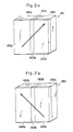
- the photosensor 141 includes, as shown in a magnified perspective view of Fig. 2a, three photodiodes 141a, 141b, and 141c which are electrically independent of each other (three-partition photodiode unit) . These photodiodes 141a to 141c are arranged in a line such that the central photodiode 141 has a light receiving surface smaller than those of the other ones. On the front surfaces respectively of the photodiodes 141a, 141b, and 141c, there are disposed analyzers 143a, 143b, and 143c, respectively.
- the photosensor 142 also includes, as can be seen from a magnified view of Fig. 2b, three photodiodes 142a, 142b, and 142c which are electrically independent of each other and which are linearly arranged so that on the front surfaces respectively of the photodiodes 142a, 142b, and 142c, there are disposed analyzers 144a, 144b, and 144c, respectively.
- the analyzers 143a to 143c arranged on the front surface of the photosensor 141 are associated with an identical polarization direction.
- the analyzers 144a to 144c disposed on the front surface of the photosensor 142 are related to an identical polarization direction.
- the polarization direction of the analyzers 143a to 143c is set to be orthogonal to that of the analyzers 144a to 144c as denoted by arrow marks respectively in Figs. 24a and 24b.
- the emission light from the semiconductor laser 131 has a polarization direction inclined by 45° with respect to each of the polarization directions respectively of the analyzers 143a to 143c and 144a to 144c.
- the photodiodes 141a, 141b, and 141c output signals having signal levels 141A, 141B, and 141C, respectively; moreover, the photodiodes 142a, 142b, and 142c are associated with signal output levels 142A, 142B, and 142C, respectively.
- a readout signal has a signal level computed as (141A + 141B + 141C) - (142A + 142B + 142C).
- the output signals from the photosensors 141 and 142 are employed to produce a focusing error signal and a tracking error signal.
- the focusing error signal is generated, for example, in a beam sizing method. Namely, the light beams received respectively by the photosensors 141 and 142 are processed so as to create therefrom signals designating magnitudes of the respective beams. Based on a signal difference therebetween, a focusing error signal is attained such that the output signal level thereof is represented as (141A + 141C - 141B) - (142A + 142C - 142B).
- the tracking error signal is produced, for example, according to a push-pull detection method.
- a push-pull detection method In this procedure, either one of the output signals respectively from the photosensors 141 and 142 is adopted for the signal generation such that the output level of the tracking error signal is represented as (141A - 141C) or (142A - 142C).
- the optical head configurations shown in Figs. 23, 24a, and 24b are applicable without any modifications thereof, where the analyzers 143a to 143c and 144a to 144c are to be omitted.
- the output signal level of the readout signal is expressed as (141A + 141B + 141C) + (142A + 142B + 142C), (141A + 141B + 141C), or (142A + 142B + 142C).
- Fig. 3 shows the structure of an optical head employed in an information recording and reproducing apparatus for a magnetooptical disk.
- the same elements and constituent components as those of Figs. 1, 2, and 2b are assigned with the same reference numerals.
- a composite beam splitter 145 having two reflection surfaces 146 and 147. These surfaces are separatedly disposed along a direction of an optical axis of the semiconductor laser 131 with an appropriate distance therebetween for the following purpose. Namely, with the provision above, it is possible to arranged in the optical axis direction a photosensor 141 located on a front side of a focal point of converged light which has been reflected from a magnetooptical disk 134 and then from the reflection surface 146 and a photosensor 142 located on a rear side of a focal point of a converged light which has been reflected from a magnetooptical disk 134 and thereafter from the reflection surface 147. Naturally, when necessary, the positions respectively of the photosensors 141 and 142 may be shifted in a direction orthogonal to the optical axis direction.
- the reflection efficiency (e.g. 9%) of the reflection surface 146 is set to be slightly smaller than that (e.g. 10%) of the reflection surface 147.
- the reflection efficiency of each surface above is almost compeltely independent of the polarization of light.
- the composite beam splitter 145 having the reflection surfaces 146 and 147 can be constituted with a combination of dielectric blocks each having reflection surfaces equivalent to the surfaces 146 and 147.
- an information readout signal, a focusing error signal, and a tracking error signal can be created in a similar manner described in conjunction with the fourth embodiment.
- the analyzers need not be disposed in the photosensors 141 and 142.
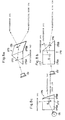
- Fig. 4 shows the configuration of an optical head of an information recording and reproducing apparatus for a magnetooptical disk in a first embodiment according to the present invention.
- the same constituent elements as that shown in Fig. 1 are assigned with the same reference numerals and a redundant description thereof will be avoided.
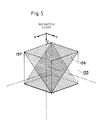
- a composite polarization beam splitter 155 including polarizing reflection surfaces 156 adn 157.
- Fig. 5 shows a magnified view of the structure of the composite polarization beam splitter 155 in which the two polarizing reflection surfaces 156 and 157 are indicated as hatching portions.
- the reflection light from a magnetooptical disk 134 is incident to the composite polarizing beam splitter 155 in a direction denoted as -Z direction.
- two directions orthogonal to the Z direction are assumed to be designated as X and Y directions, respectively.
- the polarizing reflection surface 156 is inclined by 45° relative to each of the X and Z directions whereas the polarizing reflection surface 157 is skewed by 45° relative to each of the Y and Z directions. In consequence, these surfaces 156 and 157 are disposed to be orthogonal to each other.
- Each of the polarizing reflection surfaces 156 and 157 is configured such that the reflection efficiency of an S-polarized light component (with a polarization direction parallel to the reflection surface) is set to an appropriate value not more than 100% and the transmission efficiency of a P-polarized light component is substantially 100%.
- the two orthogonal polarized light components of the reflection light from the magnetooptical disk 134 are reflected respectively by the polarizing reflection surfaces 156 and 157 to be received by the photosensors 141 and 142 respectively associated therewith.
- the photosensors 141 and 142 need not be necessarily provided with the analyzers; however, there may be adopted an analyzer for passing therethrough the polarization direction component of the incident light.
- the composite beam splitter 155 above can be constructed by combining four blocks with each other, each block having polarizing reflection surfaces coated with polarizing films, respectively.
- the polarization direction of the semiconductor laser 131 is inclined by 45° with respect to each of the two orthogonal polarization directions associated with the light polarization and separation conducted by the composite plarizing beam splitter 155.
- Fig. 6 shows the constitution of an optical pickup head of an information recording and reproducing apparatus for a magnetooptical disk.
- the same constituent elements as those of the embodiments above are assigned with the same reference numerals.
- the optical head comprises a smiconductor laser 131 and a converging optical system for focusing onto a surface of a magnetooptical disk 134 a divergent light generated from the smiconductor laser 131.
- the focusing optical system includes a collimation lens 132 for collimating the diverging light and an objective 133 for converging the collimated light.
- the configuration includes a prism 165 in an optical path of the divergent light between the semiconductor laser 131 and the collimation lens 132.
- the prism 165 is of a type easily found on the market and has two surfaces 166 and 167 each coated with a reflection film. Lights reflected from the reflection surfaces (first and second reflection surfaces) 166 and 167 are received by photosensors 141 and 142, respectively. It is favorable to set the reflection efficiency of each of these reflection surfaces such that for light incident thereto, substantially an identical quantity of light is reflected therefrom. The reflection efficiency of each reflection surface does not depend on the polarization of light.
- Divergent light created from the semiconductor laser 131 is refracted once by each of the two surfaces 166 and 167 of the prism 165 to be converged through the focusing optical system onto a surface of the magnetooptical disk 134.
- Light reflected from the disk 134 is then focused by the focusing optical system.
- a portion of the converged reflection light is reflected by the first reflection surface 166 to be incident to the photosensor 141 disposed at a position on a front side of a focusing point of the correctly focused reflection light.
- reflection light from the magnetooptical disk 134 light which has passed through the first reflection surface 166 is transmitted via the prism 165 such that a portion of the transmitted light is reflected from the second reflection surface 167 to be received by the photosensor 142 located at a position on a rear side of a focal point of the properly focused reflection light.
- the photosensors 141 and 142 are configured as shown in Figs. 2a and 2b, respectively. Moreover, as described above, based on signals produced from the photosensors 141 and 142, a data readout signal, a focusing error signal, and a tracking error signal are attained in the same manner.
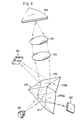
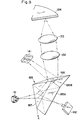
- Fig. 7 and Figs. 8a, 8b, and 8c show the configuration of an optical head of an information recording and reproducing apparatus for a magnetooptical disk in a second embodiment according to the present invention. Also in these diagrams, the same components as those shown in the above embodiments are assigned with the same reference numerals for simplification.
- a prism 175 having a considerably complex shape between a semiconductor laser 131 and a collimation lens 132.
- Figs. 8a to 8c show a plan view, a front view, and a side view of the prism 175. Furthermore, these diagrams include light proparation directions in the prism 175 of divergent light emitted from the semiconductor laser 131 and reflection light from a magnetooptical disk 134, the directions being indicated with optical axes of the respective components. Points A and B respectively denote an incident point and an emission point and a reflection point assoiciated with the divergent and reflection light.
- the prism 175 is constituted with two portions 175A and 175B.
- the portion 175A has a contour of a trigonal prism of which a surface facing the semiconductor laser 131 is assumed to be a second reflection surface 177.
- the portion 175B is a pentahedron having two lozenge-shaped surfaces, two triangular surface, and a rectangular surface.
- the portion 175B is brought into contact with the portion 175A on the rectangular surface of the portion 175B.
- One of the lozenge-shaped surfaces facing the magnetooptical disk 134 is assumed to be a first reflection surface 176.
- the reflection surfaces 176 and 177 are also constituted such that each thereof refelects substantially an identical quantity of the reflection light incident thereto so as to supply almost the same quantity of light to each of the photosensors 141 and 142.
- the reflection surfaces 176 and 177 develop functions almost completely independent of the polarization of light.
- the emission light from the prism 175 is converged onto a surface of the magnetooptical disk 134 by a focusing optical system comprising a collimation lens 132 and an objective 133.
- the light is then reflected on the optical disk 134 so that the reflection light is again converged by the focusing optical system.
- the reflection light while being thus converged, is reflected on the first reflection surface 176 (point B) to be received by a photosensor 141 located at a position on a front side of a focusing position of the reflection light appropriately focused.
- a photosensor 141 located at a position on a front side of a focusing position of the reflection light appropriately focused.
- light which has passed through the first reflection surface 176 is transmitted through the prism 175 such that a portion thereof is reflected on the second reflection surface 177 (point A).
- the reflected light is delivered through the prism 175 to be emitted from a surface of the prism portion 175A so as to be incident to a photosensor 142 disposed at a position on a rear side of the focusing position.
- an information readout signal, a focusing error signal, and a tracking error signal are generated in the same manner as for the embodiments above.
- the analyzers need not be disposed for the photosensors 141 and 142.
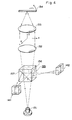
- Fig. 9 shows the configuration of an optical pickup head of an information recording and reproducing apparatus for a magnetooptical disk in a third embodiment according to the present invention.
- the same components are similarly assigned with the same reference numerals and a duplicated description thereof will be avoided.
- a prism 175 having two polarizing reflection surfaces 186 and 187 is adopted between a semiconductor laser 131 and a collimation lens 132.
- the polarizing prism 175 has a contour which is basically the same as that of the prism 165 of Fig. 7.
- the prism 175 is constituted with portions 185A and 185B and is structurally different from the prism 175 of Fig. 7 in that a polarizing film is disposed on each of the polarizing reflection surfaces 186 and 187 respectively related to the reflection surfaces 176 and 177.
- a direction Y along the first polarizing reflection surface 186 is orthogonal to a direction X along the second polarizing reflection surface 187.
- Each of the polarizing reflection surfaces 186 and 187 is constituted such that the reflection efficiency of an S-polarized light component (with a polarization direction parallel to the polarizing reflection surface) is set to an appropriate value not exceeding 100% and the transmission efficiency of a P-polarized light component is substantially 100%. Consequently, the two orthogonal polarized light components of the reflection light from the magnetooptical disk 134 are reflected respectively by the polarizing reflection surfaces 186 and 187 to enter the photosensors 141 and 142 respectively associated therewith.
- the analyzers need not necessarily be disposed for the photosensors 141 and 142; however, there may be naturally adopted an analyzer for passing therethrough the polarization direction component of the incident light.
- the reflection efficiency of the S-polarized component is favorably determined in advance for each of the polarizing reflection surfaces 186 and 187.
- the polarization direction of the semiconductor laser 131 is skewed by 45° relative to each of the two orthogonal polarization directions related to the light polarization and separation accomplished by the polarizing prism 185.
- a readout signal In this configuration of the optical pickup head, a readout signal, a focusing error signal, and a tracking error signals are also produced in the same fashion as for the embodiments above.
Landscapes
- Physics & Mathematics (AREA)
- Optics & Photonics (AREA)
- Optical Head (AREA)
- Optical Communication System (AREA)
- Glass Compositions (AREA)
- Wire Bonding (AREA)
- Led Device Packages (AREA)
- Optical Integrated Circuits (AREA)
Abstract
Description
- The present invention relates to an optical device for extracting information represented by polarized light coming from an optical object, such as an optical recording medium.
- In the present description, the optical recording medium includes in addition to an optical recording medium such as an optical disk or an optical card, a magnetooptical recording medium such as a magnetooptical disk or a magnetooptical card.
- Moreover, the optical pickup device according to the present invention may naturally be used not only to read data from the optical recording medium but also to write data thereon.
- In the prior art, an optical pickup device includes constituent elements such as a first optical system for collimating light irradiated from a semiconductor laser, a second optical system for focusing the collimated light onto an optical recording medium and for collimating light reflected from the optical recording medium, a first polarization beam splitter for separating through polarization the reflection light thus collimated by the second optical system, a second polarization beam splitter for separating the light from the first polarization beam splitter into tracking control light and focusing control light, a third optical system for focusing the separated tracking control light onto a light receiving surface of a tracking control photosensor, a fourth optical system for focusing the separated focusing control light onto a light receiving surface of a focusing control photosensor, and a fifth optical system disposed in the third or fourth optical system for guiding light to a photosensor producing a readout signal.
- The conventional optical pickup device of this type is ordinarily constituted with a large number of optical parts and hence is heavy, which leads to a problem of a slow access time. In addition, due to the large number of optical parts, the cost thereof is increased and assemblage and adjustment of these parts take a great amount of human labor and a long period of time, which also leads to the problem that the cost of the final product is increased.
- In order to solve the problems above, there have been intensive researches and studies to implement a compact and light-weight optical pickup for a magnetooptical disk based on the optical integration technology. For example, according to an optical pickup device described in an article "Waveguide-Type Differential Detection Device for Magnetooptical Disk Pickup", Sunagawa et al., Institute of Electronics, Information, and Communication Engineers of Japan, Quantum Electronics Study Group 0QE86-177, a plurality of focusing grating couplers respectively exciting light in the transverse magnetic (TM) and transverse electric (TE) modes are formed on a waveguide layer manufactured on a substrate. A light reflected from a magnetooptical disk is guided by the focusing grating couplers into the waveguide layer; moreover, the light is separated to be converged depending on the modes. The resultant reflection light is sensed so as to produce a tracking error signal, a focusing error signal, and an information readout signal.
- Fig. 10 shows the focusing grating couplers described in the article above. In the configuration, three focusing
grating couplers substrate 190. The reflection light from the magnetooptical disk is irradiated onto the focusinggrating couplers 191 to 193 from a position thereabove with a right incident angle or an oblique incident angle. These focusing grating couplers are manfactured such that thecoupler 191 has a grating period slightly larger than those of thecouplers couplers grating coupler 191, which leads to an excitation of the TM mode light. On the other hand, for the Es component thereof, the phase matching condition holds in the focusinggrating couplers grating couplers coupler 191. With this provision, the Ep and Es components of the light reflected from the magnetooptical disk are separated through thecoupler 191 and thecouplers - In the focusing grating couplers above, the two kinds of waveguide modes, namely, the TM and TE modes are excited only in the respective separated regions. More specifically, the light in the TM and TE modes is excited only in the region of the
coupler 191 and in the area of thecouplers grating couplers 191 to 193, the optical coupling of the light with the waveguide layer takes place only in some portions of the region. Consequently the quantity of the reflection light incident to the photosensors is decreased and hence it is difficult to detect various kinds of signals in a stable condition. - Furthermore, due to a variation in the wavelength of light illuminated from the light source, an increase or a decrease in the size of each grating with respect to a change in the temperature, or the like, light in other than the TM mode may be excited by the focusing
grating coupler 191 and/or the light excitation may take place for light other than the TE mode in thecouplers - In this regard, there has been also proposed a compact light-weight pickup device for an optical disk similarly employing the optical integration technology. Such a pickup device has been described, for example, in an article "An Integrated-Optic Disk Pickup Device", S. Ura et al., Institute of Electronics, Information, and Communication Engineers of Japan, Quantum Electronics Study Group 0QE85-72. Fig. 11 shows a portion of the optical pickup device. In this structure, on an SiO2
buffer layer 201 manufactured on asilicon substrate 200, awaveguide layer 202 is formed with a glass material. On thewaveguide layer 202, a focusinggrating coupler 203 and a waveguide beam splitter (grating) 204 are manufactured in a chirped structure by use of a patterning technology based on an electron beam lithography and a reactive ion etching technology. In operation, alaser diode 205 disposed on an end surface of thesubstrate 200 emits light, which propagates through thewaveguide layer 202 to be irradiated to an upward direction by the focusinggrating coupler 203 so as to be focused onto a surface of anoptical disk 209. Light reflected from the surface of theoptical disk 209 is passed via the focusinggrating coupler 203 to be optially coupled with thewaveguide 202 and is then separated by thewaveguide beam splitter 204 into two portions, which are respectively converged therethrough to be received by respective partitions of a two-partitionphotoelectric converter element 206. Based on signals created from thephotoelectric converter 206, there are generated a readout signal, a focusing error signal, and a tracking signal. In this constitution, thewaveguide beam splitter 204 develops three functions including a separation of a wave surface or wavefront, deflection of an incident light, and focusing or converging the light. Through the operation above, the system reads information recorded in the form of a pit string on a surface of theoptical disk 209. - In the optical pickup device of this kind, the light radiated from the
laser diode 205 passes twice through thewaveguide beam splitter 204 and the focusinggrating coupler 203 before the light is received by thephotoelectric converter 206, namely, the light passes these units each time the light proceeds in a direction from thelaser diode 205 to theoptical disk 209 and in a direction from thedisk 209 to thephotoelectric conversion element 206. Consequently, the light passes a grating structure four times before the light is sensed. Namely, the light received by thephotoelectric converter 206 becomes to be considerably weak and hence a signal produced therefrom has a minimized intensity. Moreover, due to an alteration in the waveform of the light emitted from the laser diode as the light source and a deviation in the period or cycle of each grating caused by a change in the temperature or the like, there particularly occurs a fluctuation in a focusing position of the light incident to thephotoelectric conversion element 206. As a result, there arises a problem that various kinds of signals cannot be sensed in a stable state. - An optical device according to the preamble of claim 1 is known from JP-A-61 003 330.
- It is therefore an object of the present invention to provide an optical device of the type above for an optical pickup device in which a tracking error signal, a focusing error signal, and an information readout signal are obtained with a high stability and an increased accuracy.
- In accordance with the present invention, there is provided an optical device as defined in claim 1.
-
- Fig. 1 is a schematic diagram showing the constitution of an optical system used in an optical pickup head of an information recording and reproducing apparatus for a magnetooptical disk;
- Figs. 2a and 2b are perspective views showing the configuration of a photosensor;
- Fig. 3 is a diagram showing the structure of an optical system adopted in an optical pickup head of an information recording and reproducing apparatus for a magnetooptical disk ;
- Fig. 4 is a schematic diagram showing the construction of an optical system adopted in an optical pickup head of an information recording and reproducing apparatus for a magnetooptical disk in a first embodiment according to the present invention;
- Fig. 5 is a magnified perspective view showing a composite polarization beam splitter utilized in the optical system of the first embodiment;
- Fig. 6 is a diagram showing the constitution of an optical system employed in an optical pickup head of an information recording and reproducing apparatus for a magnetooptical disk ;
- Fig 7 is a diagram showing the configuration of an optical system used in an-optical pickup head of an information recording and reproducing apparatus for a magnetooptical disk in a second embodiment according to the present invention;
- Figs. 8a, 8b, and 8c are a plan view, a front view, and a side view of a prism utilized in the optical head of Fig. 29;
- Fig. 9 is a perspective view illustratively showing the structure of an optical system used in an optical pickup head of an information recording and reproducing apparatus for a magnetooptical disk in a third embodiment according to the present invention;
- Fig. 10 is a plan view schematically showing a grating coupler adopted in a conventional optical pickup device; and
- Fig. 11 is a perspective view showing an optical system of a conventional optical pickup device.
- Fig. 1 and Figs. 2a and 2b show a schematic diagram showing an optical pickup device, that is the constitution of an optical pickup head used to record information on and to read information a magnetooptical disk.
- The optical head includes a
semiconductor laser 131 and a focusing optical system for converging onto a surface of amagnetooptical disk 134 divergent light emitted from thelaser 131. The optical system comprises acollimation lens 132 for collimating the emitted light and an objective 133 for converging the collimated light. - A
composite beam splitter 135 is disposed in an optical path of the divergent light between thesemiconductor laser 131 andtne collimation lens 132. Thecomposite beam splitter 135 has tworeflection surfaces - The
compsite beam splitter 135 may be constituted with four dielectric blocks (e.g. glass prisms). Each of the blocks includes surfaces respectively coated with reflection films so as to develop functions respectively of the reflection surfaces 136 and 137. The combined four dielectric blocks are bonded to each other. The reflection surfaces 136 and 137 are configured so as to pass therethrough to a possible extent the emission light from thesemiconductor laser 131 and to refiect a portion (for example, 10%) of a light reflected from themagnetooptical disk 134. In this regard, the optical reflection efficiency of each of the reflection surfaces 136 and 137 does not depend on the polarization of light. - The divergent light produced from the
semiconductor laser 131 is transmitted through thecomposite beam splitter 135 to be converged by the focusing optical system onto themagnetooptical disk 134. Light reflected from thedisk 134 is converged by the focusing optical system. While the reflection light is being converged through the optical system, portions thereof are reflected by the reflection surfaces 136 and 137 of thecomposite beam splitter 135, respectively. The reflected light is then respectively received byphotosensors - The
photosensor 141 includes, as shown in a magnified perspective view of Fig. 2a, threephotodiodes photodiodes 141a to 141c are arranged in a line such that thecentral photodiode 141 has a light receiving surface smaller than those of the other ones. On the front surfaces respectively of thephotodiodes - The
photosensor 142 also includes, as can be seen from a magnified view of Fig. 2b, threephotodiodes photodiodes - The
analyzers 143a to 143c arranged on the front surface of the photosensor 141 are associated with an identical polarization direction. Moreover, theanalyzers 144a to 144c disposed on the front surface of the photosensor 142 are related to an identical polarization direction. The polarization direction of theanalyzers 143a to 143c is set to be orthogonal to that of theanalyzers 144a to 144c as denoted by arrow marks respectively in Figs. 24a and 24b. The emission light from thesemiconductor laser 131 has a polarization direction inclined by 45° with respect to each of the polarization directions respectively of theanalyzers 143a to 143c and 144a to 144c. - Let us assume here that the
photodiodes photodiodes magnetooptical disk 134 is read therefrom, a readout signal has a signal level computed as (141A + 141B + 141C) - (142A + 142B + 142C). - Moreover, the output signals from the
photosensors - The focusing error signal is generated, for example, in a beam sizing method. Namely, the light beams received respectively by the
photosensors - Moreover, the tracking error signal is produced, for example, according to a push-pull detection method. In this procedure, either one of the output signals respectively from the
photosensors - When the optical recording medium is impiemeted in the form of, for example, an optical disk or an optical card, the optical head configurations shown in Figs. 23, 24a, and 24b are applicable without any modifications thereof, where the
analyzers 143a to 143c and 144a to 144c are to be omitted. In this situation, the output signal level of the readout signal is expressed as (141A + 141B + 141C) + (142A + 142B + 142C), (141A + 141B + 141C), or (142A + 142B + 142C). - Fig. 3 shows the structure of an optical head employed in an information recording and reproducing apparatus for a magnetooptical disk. In this diagram, the same elements and constituent components as those of Figs. 1, 2, and 2b are assigned with the same reference numerals.
- Between a
semiconductor laser 131 and acollimation lens 132, there is arranged acomposite beam splitter 145 having tworeflection surfaces semiconductor laser 131 with an appropriate distance therebetween for the following purpose. Namely, with the provision above, it is possible to arranged in the optical axis direction a photosensor 141 located on a front side of a focal point of converged light which has been reflected from amagnetooptical disk 134 and then from thereflection surface 146 and a photosensor 142 located on a rear side of a focal point of a converged light which has been reflected from amagnetooptical disk 134 and thereafter from thereflection surface 147. Naturally, when necessary, the positions respectively of thephotosensors - Of the reflection light from the
magnetooptical disk 134, only a light which has passed through thereflection surface 146 and which has reflected from thereflection surface 147 is received by thephotosensor 142. In order to substantially equalize to each other the quantities of light to be respectively received by thephotosensors reflection surface 146 is set to be slightly smaller than that (e.g. 10%) of thereflection surface 147. The reflection efficiency of each surface above is almost compeltely independent of the polarization of light. Thecomposite beam splitter 145 having the reflection surfaces 146 and 147 can be constituted with a combination of dielectric blocks each having reflection surfaces equivalent to thesurfaces - In the optical pickup head above, an information readout signal, a focusing error signal, and a tracking error signal can be created in a similar manner described in conjunction with the fourth embodiment.
- Moreover, when an optical disk or the like is employed as the optical-recording medium, it is natural that the analyzers need not be disposed in the
photosensors - Fig. 4 shows the configuration of an optical head of an information recording and reproducing apparatus for a magnetooptical disk in a first embodiment according to the present invention. In this constitution, the same constituent elements as that shown in Fig. 1 are assigned with the same reference numerals and a redundant description thereof will be avoided.
- Between a
semiconductor laser 131 and acollimation lens 132, there is disposed a compositepolarization beam splitter 155 including polarizing reflection surfaces 156adn 157. Fig. 5 shows a magnified view of the structure of the compositepolarization beam splitter 155 in which the two polarizing reflection surfaces 156 and 157 are indicated as hatching portions. - In this diagram, let us assume that the reflection light from a
magnetooptical disk 134 is incident to the compositepolarizing beam splitter 155 in a direction denoted as -Z direction. As shown here, two directions orthogonal to the Z direction are assumed to be designated as X and Y directions, respectively. Thepolarizing reflection surface 156 is inclined by 45° relative to each of the X and Z directions whereas thepolarizing reflection surface 157 is skewed by 45° relative to each of the Y and Z directions. In consequence, thesesurfaces - Each of the polarizing reflection surfaces 156 and 157 is configured such that the reflection efficiency of an S-polarized light component (with a polarization direction parallel to the reflection surface) is set to an appropriate value not more than 100% and the transmission efficiency of a P-polarized light component is substantially 100%. In consequence, the two orthogonal polarized light components of the reflection light from the
magnetooptical disk 134 are reflected respectively by the polarizing reflection surfaces 156 and 157 to be received by thephotosensors photosensors - The
composite beam splitter 155 above can be constructed by combining four blocks with each other, each block having polarizing reflection surfaces coated with polarizing films, respectively. - The polarization direction of the
semiconductor laser 131 is inclined by 45° with respect to each of the two orthogonal polarization directions associated with the light polarization and separation conducted by the compositeplarizing beam splitter 155. - Also in this configuration, a readout signal, a focusing error signal, and a tracking error signals are obtained in the same fashion as for the embodiments above.
- Fig. 6 shows the constitution of an optical pickup head of an information recording and reproducing apparatus for a magnetooptical disk. In the structure of this embodiment, the same constituent elements as those of the embodiments above are assigned with the same reference numerals.
- The optical head comprises a
smiconductor laser 131 and a converging optical system for focusing onto a surface of a magnetooptical disk 134 a divergent light generated from thesmiconductor laser 131. The focusing optical system includes acollimation lens 132 for collimating the diverging light and an objective 133 for converging the collimated light. - The configuration includes a
prism 165 in an optical path of the divergent light between thesemiconductor laser 131 and thecollimation lens 132. Theprism 165 is of a type easily found on the market and has twosurfaces photosensors - Divergent light created from the
semiconductor laser 131 is refracted once by each of the twosurfaces prism 165 to be converged through the focusing optical system onto a surface of themagnetooptical disk 134. Light reflected from thedisk 134 is then focused by the focusing optical system. A portion of the converged reflection light is reflected by thefirst reflection surface 166 to be incident to the photosensor 141 disposed at a position on a front side of a focusing point of the correctly focused reflection light. Of the reflection light from themagnetooptical disk 134, light which has passed through thefirst reflection surface 166 is transmitted via theprism 165 such that a portion of the transmitted light is reflected from thesecond reflection surface 167 to be received by thephotosensor 142 located at a position on a rear side of a focal point of the properly focused reflection light. - The
photosensors photosensors - Fig. 7 and Figs. 8a, 8b, and 8c show the configuration of an optical head of an information recording and reproducing apparatus for a magnetooptical disk in a second embodiment according to the present invention. Also in these diagrams, the same components as those shown in the above embodiments are assigned with the same reference numerals for simplification.
- In the constitution, there is disposed a
prism 175 having a considerably complex shape between asemiconductor laser 131 and acollimation lens 132. - For an easy understanding of the complicated shape of the
prism 175, Figs. 8a to 8c show a plan view, a front view, and a side view of theprism 175. Furthermore, these diagrams include light proparation directions in theprism 175 of divergent light emitted from thesemiconductor laser 131 and reflection light from amagnetooptical disk 134, the directions being indicated with optical axes of the respective components. Points A and B respectively denote an incident point and an emission point and a reflection point assoiciated with the divergent and reflection light. - For simplification, let us consider that the
prism 175 is constituted with twoportions portion 175A has a contour of a trigonal prism of which a surface facing thesemiconductor laser 131 is assumed to be asecond reflection surface 177. Theportion 175B is a pentahedron having two lozenge-shaped surfaces, two triangular surface, and a rectangular surface. Theportion 175B is brought into contact with theportion 175A on the rectangular surface of theportion 175B. One of the lozenge-shaped surfaces facing themagnetooptical disk 134 is assumed to be afirst reflection surface 176. The reflection surfaces 176 and 177 are also constituted such that each thereof refelects substantially an identical quantity of the reflection light incident thereto so as to supply almost the same quantity of light to each of thephotosensors - Diverging light illuminated from the
semiconductor laser 131 enters theprism 175 from thesecond reflection surface 177. (point A) of theprism 175 to be refracted therein and is then emitted from the first surface 176 (point B) of theprism 175. The emission light from theprism 175 is converged onto a surface of themagnetooptical disk 134 by a focusing optical system comprising acollimation lens 132 and an objective 133. The light is then reflected on theoptical disk 134 so that the reflection light is again converged by the focusing optical system. The reflection light, while being thus converged, is reflected on the first reflection surface 176 (point B) to be received by aphotosensor 141 located at a position on a front side of a focusing position of the reflection light appropriately focused. Moreover, of the light reflected from themagnetooptical disk 134, light which has passed through thefirst reflection surface 176 is transmitted through theprism 175 such that a portion thereof is reflected on the second reflection surface 177 (point A). The reflected light is delivered through theprism 175 to be emitted from a surface of theprism portion 175A so as to be incident to a photosensor 142 disposed at a position on a rear side of the focusing position. - In this opitcal pickup head, an information readout signal, a focusing error signal, and a tracking error signal are generated in the same manner as for the embodiments above.
- In a case where an optical disk or the like is utilized as the optical recording medium, it is to be understood that the analyzers need not be disposed for the
photosensors - Fig. 9 shows the configuration of an optical pickup head of an information recording and reproducing apparatus for a magnetooptical disk in a third embodiment according to the present invention. In this diagram, the same components are similarly assigned with the same reference numerals and a duplicated description thereof will be avoided.
- In the constitution, a
prism 175 having two polarizing reflection surfaces 186 and 187 is adopted between asemiconductor laser 131 and acollimation lens 132. Thepolarizing prism 175 has a contour which is basically the same as that of theprism 165 of Fig. 7. Theprism 175 is constituted withportions prism 175 of Fig. 7 in that a polarizing film is disposed on each of the polarizing reflection surfaces 186 and 187 respectively related to the reflection surfaces 176 and 177. Moreover, as can be seen from Fig. 9, a direction Y along the firstpolarizing reflection surface 186 is orthogonal to a direction X along the secondpolarizing reflection surface 187. - Each of the polarizing reflection surfaces 186 and 187 is constituted such that the reflection efficiency of an S-polarized light component (with a polarization direction parallel to the polarizing reflection surface) is set to an appropriate value not exceeding 100% and the transmission efficiency of a P-polarized light component is substantially 100%. Consequently, the two orthogonal polarized light components of the reflection light from the
magnetooptical disk 134 are reflected respectively by the polarizing reflection surfaces 186 and 187 to enter thephotosensors photosensors - It is naturally to be understood that in order to substantially equalize to each other the reflection light quantities to be incident to the two
photosensors - The polarization direction of the
semiconductor laser 131 is skewed by 45° relative to each of the two orthogonal polarization directions related to the light polarization and separation accomplished by thepolarizing prism 185. - In this configuration of the optical pickup head, a readout signal, a focusing error signal, and a tracking error signals are also produced in the same fashion as for the embodiments above.
Claims (10)
- An optical device for extracting information represented by polarized light coming from an optical magneto-optical recording medium (134), the optical device comprising a composite polarizing beam splitter (155, 175, 185) having two reflection surfaces (156, 157, 176, 177, 186, 187) for reflecting a portion of the polarized light from the recording medium, and further comprising two photosensors (141, 142) for respectively receiving two light beams reflected from said composite beam splitter,
charcterized in thatsaid composite polarizing beam splitter (155, 175, 185) has two polarizing reflection surfaces (156, 157, 176, 177, 186, 187) for separating a portion of the polarized light from the recording medium into two polarized reflection light components having directions of polarization orthogonal to each other and for reflecting these polarized reflection light components into two different directions, andsaid two photosensors (141, 142) are respectively receiving said two polarized light components separated by said composite polarization beam splitter. - An optical device in accordance with claim 1 characterized in that said two polarizing reflection surfaces (156, 157) of said composite polarization beam splitter (155) are substantially orthogonal to each other.
- An optical device in accordance with claim 1 characterized in that said two reflection surfaces (176, 177, 186, 187) are disposed along a direction of an optical axis of the polarized light from the recording medium (134).
- An optical device in accordance with claim 1 characterized in that said composite beams splitter is a prism (185) having said two polarization reflection surfaces (186, 187) as surfaces thereof.
- An optical device in accordance with claim 4 characterized in that said polarization reflection surfaces (186, 187) of said prism (185) are orthogonal to each other.
- An optical device in accordance with claim 1 or 4 characterized in that said optical device further comprises;a light emitting element (131); anda focusing optical system (132, 133) for converging light irradiated from said light emitting element onto said recording medium (134) and for focusing reflection light from said recording mediumwherein said composite beam splitter (155, 175, 185) passes therethrough at least a portion of the light emitted from said light emitting element, and the polarized light from the recording medium is light reflected from the recording medium.
- An optical device in accordance with claim 6 characterized in that said focusing optical system (132, 133) is disposed between said composite polarization beam splitter (155, 175, 185) and the recording medium.
- An optical device in accordance with claim 6 characterized in that said composite beam splitter (155, 175, 185) is disposed between said light emitting element (131) and said focusing optical system (132, 133).
- An optical device in accordance with claim 8 characterized in thatsaid focusing optical system includes a collimation lens (132) and an objective (133), andsaid collimation lens (132) is disposed between said objective (133) and said composite beam splitter (155, 175, 185).
- An optical device in accordance with claim 1 characterized in that said optical device further includes two analyzers (143a, 143b, 143c, 144a, 144b, 144c) respectively disposed on front sides of said photosensors (141, 142), said analyzers respectively having polarization directions which are orthogonal to each other.
Applications Claiming Priority (10)
| Application Number | Priority Date | Filing Date | Title |
|---|---|---|---|
| JP2204367A JPH0488305A (en) | 1990-07-31 | 1990-07-31 | Optical pickup device |
| JP204367/90 | 1990-07-31 | ||
| JP201450/90 | 1990-07-31 | ||
| JP20145090 | 1990-07-31 | ||
| JP25007990A JPH04176040A (en) | 1990-07-31 | 1990-09-21 | Optical pick-up device |
| JP250079/90 | 1990-09-21 | ||
| JP3074196A JPH04286746A (en) | 1991-03-15 | 1991-03-15 | optical pickup device |
| JP3074195A JPH04286745A (en) | 1991-03-15 | 1991-03-15 | Optical pickup device |
| JP74195/91 | 1991-03-15 | ||
| JP74196/91 | 1991-03-15 |
Publications (3)
| Publication Number | Publication Date |
|---|---|
| EP0469552A2 EP0469552A2 (en) | 1992-02-05 |
| EP0469552A3 EP0469552A3 (en) | 1993-01-13 |
| EP0469552B1 true EP0469552B1 (en) | 1997-07-09 |
Family
ID=27524492
Family Applications (1)
| Application Number | Title | Priority Date | Filing Date |
|---|---|---|---|
| EP91112802A Expired - Lifetime EP0469552B1 (en) | 1990-07-31 | 1991-07-30 | Optical pickup device |
Country Status (3)
| Country | Link |
|---|---|
| EP (1) | EP0469552B1 (en) |
| AT (1) | ATE155275T1 (en) |
| DE (1) | DE69126745T2 (en) |
Families Citing this family (5)
| Publication number | Priority date | Publication date | Assignee | Title |
|---|---|---|---|---|
| US5410468A (en) * | 1992-06-26 | 1995-04-25 | Matsushita Electric Industrial Co., Ltd. | Optical pick-up apparatus |
| DE69318770T2 (en) * | 1992-07-30 | 1998-10-15 | Matsushita Electric Ind Co Ltd | Optical playback device |
| JPH06195728A (en) * | 1992-12-24 | 1994-07-15 | Matsushita Electric Ind Co Ltd | Optical head |
| JP3635523B2 (en) * | 1999-02-03 | 2005-04-06 | パイオニア株式会社 | Optical waveguide device and optical pickup |
| US7171080B2 (en) | 2004-11-15 | 2007-01-30 | Seagate Technology Llc | Coupling grating for focusing light within a waveguide for heat assisted magnetic recording |
Family Cites Families (2)
| Publication number | Priority date | Publication date | Assignee | Title |
|---|---|---|---|---|
| EP0174008B1 (en) * | 1984-09-03 | 1992-05-20 | Omron Tateisi Electronics Co. | Device for processing optical data |
| JPH0622065B2 (en) * | 1987-02-25 | 1994-03-23 | 株式会社日立製作所 | Integrated optical head |
-
1991
- 1991-07-30 EP EP91112802A patent/EP0469552B1/en not_active Expired - Lifetime
- 1991-07-30 AT AT91112802T patent/ATE155275T1/en active
- 1991-07-30 DE DE69126745T patent/DE69126745T2/en not_active Expired - Fee Related
Also Published As
| Publication number | Publication date |
|---|---|
| EP0469552A3 (en) | 1993-01-13 |
| EP0469552A2 (en) | 1992-02-05 |
| DE69126745D1 (en) | 1997-08-14 |
| DE69126745T2 (en) | 1998-02-26 |
| ATE155275T1 (en) | 1997-07-15 |
Similar Documents
| Publication | Publication Date | Title |
|---|---|---|
| EP0306342B1 (en) | Optical information processing apparatus | |
| US4876680A (en) | Monolithic optical pick-up using an optical waveguide | |
| US5278817A (en) | Optical pick-up for use with an opto-magnetic signal | |
| EP0557017B1 (en) | Optical disk apparatus | |
| US5835472A (en) | Optical pickup device with substantially mutually orthogonal reflection surfaces | |
| US4935911A (en) | Optical head device for recording and reproducing information | |
| US5095472A (en) | Focusing error detecting system for optical head | |
| EP0469552B1 (en) | Optical pickup device | |
| CA2002586C (en) | Autofocus system | |
| US4954702A (en) | Process for detecting a focal point in an optical head | |
| JP3067906B2 (en) | Optical pickup device | |
| JPH04252444A (en) | optical pickup device | |
| JPH07169090A (en) | Optical information parallel recording / reproducing device | |
| JPH09171633A (en) | Integrated optical pickup system | |
| JP2513237B2 (en) | Optical head device | |
| JP3545794B2 (en) | Waveguide type optical signal detector | |
| JP4072776B2 (en) | Optical pick-up module and magneto-optical signal recording / reproducing apparatus | |
| JP3499918B2 (en) | Magneto-optical information recording / reproducing device | |
| JPH0786981B2 (en) | Optical information processing device | |
| JPH06150425A (en) | Optical pickup | |
| JPH04209339A (en) | optical pickup device | |
| JPS63148448A (en) | Magneto-optical head device | |
| JPH04286745A (en) | Optical pickup device | |
| JPH0495252A (en) | optical reader | |
| JPH0798882A (en) | Optical pickup device |
Legal Events
| Date | Code | Title | Description |
|---|---|---|---|
| PUAI | Public reference made under article 153(3) epc to a published international application that has entered the european phase |
Free format text: ORIGINAL CODE: 0009012 |
|
| 17P | Request for examination filed |
Effective date: 19910827 |
|
| AK | Designated contracting states |
Kind code of ref document: A2 Designated state(s): AT BE CH DE DK ES FR GB GR IT LI NL SE |
|
| PUAL | Search report despatched |
Free format text: ORIGINAL CODE: 0009013 |
|
| AK | Designated contracting states |
Kind code of ref document: A3 Designated state(s): AT BE CH DE DK ES FR GB GR IT LI NL SE |
|
| 17Q | First examination report despatched |
Effective date: 19940922 |
|
| GRAG | Despatch of communication of intention to grant |
Free format text: ORIGINAL CODE: EPIDOS AGRA |
|
| GRAH | Despatch of communication of intention to grant a patent |
Free format text: ORIGINAL CODE: EPIDOS IGRA |
|
| GRAH | Despatch of communication of intention to grant a patent |
Free format text: ORIGINAL CODE: EPIDOS IGRA |
|
| GRAA | (expected) grant |
Free format text: ORIGINAL CODE: 0009210 |
|
| AK | Designated contracting states |
Kind code of ref document: B1 Designated state(s): AT BE CH DE DK ES FR GB GR IT LI NL SE |
|
| PG25 | Lapsed in a contracting state [announced via postgrant information from national office to epo] |
Ref country code: IT Free format text: LAPSE BECAUSE OF FAILURE TO SUBMIT A TRANSLATION OF THE DESCRIPTION OR TO PAY THE FEE WITHIN THE PRE;WARNING: LAPSES OF ITALIAN PATENTS WITH EFFECTIVE DATE BEFORE 2007 MAY HAVE OCCURRED AT ANY TIME BEFORE 2007. THE CORRECT EFFECTIVE DATE MAY BE DIFFERENT FROM THE ONE RECORDED.SCRIBED TIME-LIMIT Effective date: 19970709 Ref country code: NL Free format text: LAPSE BECAUSE OF FAILURE TO SUBMIT A TRANSLATION OF THE DESCRIPTION OR TO PAY THE FEE WITHIN THE PRESCRIBED TIME-LIMIT Effective date: 19970709 Ref country code: LI Free format text: LAPSE BECAUSE OF FAILURE TO SUBMIT A TRANSLATION OF THE DESCRIPTION OR TO PAY THE FEE WITHIN THE PRESCRIBED TIME-LIMIT Effective date: 19970709 Ref country code: GR Free format text: LAPSE BECAUSE OF FAILURE TO SUBMIT A TRANSLATION OF THE DESCRIPTION OR TO PAY THE FEE WITHIN THE PRESCRIBED TIME-LIMIT Effective date: 19970709 Ref country code: FR Effective date: 19970709 Ref country code: AT Effective date: 19970709 Ref country code: BE Effective date: 19970709 Ref country code: CH Free format text: LAPSE BECAUSE OF FAILURE TO SUBMIT A TRANSLATION OF THE DESCRIPTION OR TO PAY THE FEE WITHIN THE PRESCRIBED TIME-LIMIT Effective date: 19970709 Ref country code: ES Free format text: THE PATENT HAS BEEN ANNULLED BY A DECISION OF A NATIONAL AUTHORITY Effective date: 19970709 Ref country code: DK Effective date: 19970709 |
|
| REF | Corresponds to: |
Ref document number: 155275 Country of ref document: AT Date of ref document: 19970715 Kind code of ref document: T |
|
| REG | Reference to a national code |
Ref country code: CH Ref legal event code: EP |
|
| REF | Corresponds to: |
Ref document number: 69126745 Country of ref document: DE Date of ref document: 19970814 |
|
| PG25 | Lapsed in a contracting state [announced via postgrant information from national office to epo] |
Ref country code: SE Effective date: 19971009 Ref country code: GB Free format text: LAPSE BECAUSE OF NON-PAYMENT OF DUE FEES Effective date: 19971009 |
|
| NLV1 | Nl: lapsed or annulled due to failure to fulfill the requirements of art. 29p and 29m of the patents act | ||
| EN | Fr: translation not filed | ||
| REG | Reference to a national code |
Ref country code: CH Ref legal event code: PL |
|
| PLBE | No opposition filed within time limit |
Free format text: ORIGINAL CODE: 0009261 |
|
| STAA | Information on the status of an ep patent application or granted ep patent |
Free format text: STATUS: NO OPPOSITION FILED WITHIN TIME LIMIT |
|
| GBPC | Gb: european patent ceased through non-payment of renewal fee |
Effective date: 19971009 |
|
| 26N | No opposition filed | ||
| PGFP | Annual fee paid to national office [announced via postgrant information from national office to epo] |
Ref country code: DE Payment date: 20080731 Year of fee payment: 18 |
|
| PG25 | Lapsed in a contracting state [announced via postgrant information from national office to epo] |
Ref country code: DE Free format text: LAPSE BECAUSE OF NON-PAYMENT OF DUE FEES Effective date: 20100202 |
|
| REG | Reference to a national code |
Ref country code: DE Ref legal event code: R082 Ref document number: 69126745 Country of ref document: DE Representative=s name: KILIAN KILIAN & PARTNER, DE |