EP0468897A1 - Process for the determination of the complete removal of a thin film on a non-planar substrate - Google Patents
Process for the determination of the complete removal of a thin film on a non-planar substrate Download PDFInfo
- Publication number
- EP0468897A1 EP0468897A1 EP91420256A EP91420256A EP0468897A1 EP 0468897 A1 EP0468897 A1 EP 0468897A1 EP 91420256 A EP91420256 A EP 91420256A EP 91420256 A EP91420256 A EP 91420256A EP 0468897 A1 EP0468897 A1 EP 0468897A1
- Authority
- EP
- European Patent Office
- Prior art keywords
- thin layer
- substrate
- diffraction grating
- diffraction
- layer
- Prior art date
- Legal status (The legal status is an assumption and is not a legal conclusion. Google has not performed a legal analysis and makes no representation as to the accuracy of the status listed.)
- Granted
Links
- 238000000034 method Methods 0.000 title claims abstract description 18
- 239000000758 substrate Substances 0.000 title claims abstract description 18
- 239000010409 thin film Substances 0.000 title 1
- 238000005530 etching Methods 0.000 claims abstract description 35
- 239000000463 material Substances 0.000 claims abstract description 4
- 230000003287 optical effect Effects 0.000 claims abstract description 4
- 230000008030 elimination Effects 0.000 claims description 5
- 238000003379 elimination reaction Methods 0.000 claims description 5
- VYPSYNLAJGMNEJ-UHFFFAOYSA-N Silicium dioxide Chemical compound O=[Si]=O VYPSYNLAJGMNEJ-UHFFFAOYSA-N 0.000 claims description 4
- 229910052814 silicon oxide Inorganic materials 0.000 claims description 4
- 239000002184 metal Substances 0.000 description 22
- 238000004519 manufacturing process Methods 0.000 description 5
- 238000001514 detection method Methods 0.000 description 2
- 238000011065 in-situ storage Methods 0.000 description 2
- 238000005259 measurement Methods 0.000 description 2
- 230000002035 prolonged effect Effects 0.000 description 2
- 241001080024 Telles Species 0.000 description 1
- 230000001066 destructive effect Effects 0.000 description 1
- 229910052734 helium Inorganic materials 0.000 description 1
- 239000001307 helium Substances 0.000 description 1
- SWQJXJOGLNCZEY-UHFFFAOYSA-N helium atom Chemical compound [He] SWQJXJOGLNCZEY-UHFFFAOYSA-N 0.000 description 1
- 239000011810 insulating material Substances 0.000 description 1
- 238000012986 modification Methods 0.000 description 1
- 230000004048 modification Effects 0.000 description 1
- 229910052754 neon Inorganic materials 0.000 description 1
- GKAOGPIIYCISHV-UHFFFAOYSA-N neon atom Chemical compound [Ne] GKAOGPIIYCISHV-UHFFFAOYSA-N 0.000 description 1
- 238000005070 sampling Methods 0.000 description 1
- 239000007787 solid Substances 0.000 description 1
- 238000001228 spectrum Methods 0.000 description 1
- 235000012431 wafers Nutrition 0.000 description 1
Images
Classifications
-
- B—PERFORMING OPERATIONS; TRANSPORTING
- B24—GRINDING; POLISHING
- B24B—MACHINES, DEVICES, OR PROCESSES FOR GRINDING OR POLISHING; DRESSING OR CONDITIONING OF ABRADING SURFACES; FEEDING OF GRINDING, POLISHING, OR LAPPING AGENTS
- B24B37/00—Lapping machines or devices; Accessories
- B24B37/005—Control means for lapping machines or devices
- B24B37/013—Devices or means for detecting lapping completion
-
- H—ELECTRICITY
- H01—ELECTRIC ELEMENTS
- H01J—ELECTRIC DISCHARGE TUBES OR DISCHARGE LAMPS
- H01J37/00—Discharge tubes with provision for introducing objects or material to be exposed to the discharge, e.g. for the purpose of examination or processing thereof
- H01J37/32—Gas-filled discharge tubes
- H01J37/32917—Plasma diagnostics
- H01J37/32935—Monitoring and controlling tubes by information coming from the object and/or discharge
- H01J37/32963—End-point detection
-
- H—ELECTRICITY
- H01—ELECTRIC ELEMENTS
- H01L—SEMICONDUCTOR DEVICES NOT COVERED BY CLASS H10
- H01L21/00—Processes or apparatus adapted for the manufacture or treatment of semiconductor or solid state devices or of parts thereof
- H01L21/02—Manufacture or treatment of semiconductor devices or of parts thereof
- H01L21/04—Manufacture or treatment of semiconductor devices or of parts thereof the devices having potential barriers, e.g. a PN junction, depletion layer or carrier concentration layer
- H01L21/18—Manufacture or treatment of semiconductor devices or of parts thereof the devices having potential barriers, e.g. a PN junction, depletion layer or carrier concentration layer the devices having semiconductor bodies comprising elements of Group IV of the Periodic Table or AIIIBV compounds with or without impurities, e.g. doping materials
- H01L21/30—Treatment of semiconductor bodies using processes or apparatus not provided for in groups H01L21/20 - H01L21/26
- H01L21/31—Treatment of semiconductor bodies using processes or apparatus not provided for in groups H01L21/20 - H01L21/26 to form insulating layers thereon, e.g. for masking or by using photolithographic techniques; After treatment of these layers; Selection of materials for these layers
- H01L21/3205—Deposition of non-insulating-, e.g. conductive- or resistive-, layers on insulating layers; After-treatment of these layers
- H01L21/321—After treatment
- H01L21/3213—Physical or chemical etching of the layers, e.g. to produce a patterned layer from a pre-deposited extensive layer
- H01L21/32133—Physical or chemical etching of the layers, e.g. to produce a patterned layer from a pre-deposited extensive layer by chemical means only
- H01L21/32135—Physical or chemical etching of the layers, e.g. to produce a patterned layer from a pre-deposited extensive layer by chemical means only by vapour etching only
- H01L21/32136—Physical or chemical etching of the layers, e.g. to produce a patterned layer from a pre-deposited extensive layer by chemical means only by vapour etching only using plasmas
- H01L21/32137—Physical or chemical etching of the layers, e.g. to produce a patterned layer from a pre-deposited extensive layer by chemical means only by vapour etching only using plasmas of silicon-containing layers
-
- H—ELECTRICITY
- H01—ELECTRIC ELEMENTS
- H01L—SEMICONDUCTOR DEVICES NOT COVERED BY CLASS H10
- H01L21/00—Processes or apparatus adapted for the manufacture or treatment of semiconductor or solid state devices or of parts thereof
- H01L21/70—Manufacture or treatment of devices consisting of a plurality of solid state components formed in or on a common substrate or of parts thereof; Manufacture of integrated circuit devices or of parts thereof
- H01L21/71—Manufacture of specific parts of devices defined in group H01L21/70
- H01L21/768—Applying interconnections to be used for carrying current between separate components within a device comprising conductors and dielectrics
- H01L21/76838—Applying interconnections to be used for carrying current between separate components within a device comprising conductors and dielectrics characterised by the formation and the after-treatment of the conductors
- H01L21/76877—Filling of holes, grooves or trenches, e.g. vias, with conductive material
-
- H—ELECTRICITY
- H01—ELECTRIC ELEMENTS
- H01L—SEMICONDUCTOR DEVICES NOT COVERED BY CLASS H10
- H01L22/00—Testing or measuring during manufacture or treatment; Reliability measurements, i.e. testing of parts without further processing to modify the parts as such; Structural arrangements therefor
- H01L22/20—Sequence of activities consisting of a plurality of measurements, corrections, marking or sorting steps
- H01L22/26—Acting in response to an ongoing measurement without interruption of processing, e.g. endpoint detection, in-situ thickness measurement
-
- H—ELECTRICITY
- H01—ELECTRIC ELEMENTS
- H01J—ELECTRIC DISCHARGE TUBES OR DISCHARGE LAMPS
- H01J2237/00—Discharge tubes exposing object to beam, e.g. for analysis treatment, etching, imaging
- H01J2237/30—Electron or ion beam tubes for processing objects
- H01J2237/304—Controlling tubes
- H01J2237/30466—Detecting endpoint of process
-
- H—ELECTRICITY
- H01—ELECTRIC ELEMENTS
- H01J—ELECTRIC DISCHARGE TUBES OR DISCHARGE LAMPS
- H01J2237/00—Discharge tubes exposing object to beam, e.g. for analysis treatment, etching, imaging
- H01J2237/32—Processing objects by plasma generation
- H01J2237/33—Processing objects by plasma generation characterised by the type of processing
- H01J2237/334—Etching
Definitions
- the present invention relates to a method for detecting the end of attack, and more particularly the complete removal, of a layer deposited on a substrate.
- the invention finds applications in the field of manufacturing integrated circuits, in particular for detecting the end of the attack of a thin metallic layer deposited on a substrate having a certain relief.
- An object of the present invention is to provide a method for the precise determination of the complete elimination of a thin layer deposited on a substrate.
- Another object of the present invention is to provide such a method which can be used as a means of control to verify that an etching operation has been carried out in a satisfactory manner.
- Another object of the present invention is to provide such a method which can be implemented in situ during an etching operation.
- the invention provides a method for determining the complete elimination of a thin layer deposited on a substrate, comprising the steps consisting in providing on an area of substrate an optical diffraction grating, the thin layer deposited on the substrate also covering this diffraction grating, and the attack of the thin layer also taking place at the level of this diffraction grating; illuminate the network with a monochromatic light beam; and observing the evolution of the diffracted light during the etching operation of the thin layer, in order to determine the instant when the material of the thin layer is completely removed.
- the substrate corresponds to a layer of silicon oxide
- the diffraction grating is obtained by anisotropic etching of a determined area of this layer
- the thin layer is metallic
- the diffraction pattern obtained from the grating is compared to diffraction patterns obtained during a calibration.
- a first metal layer is deposited which is etched according to a chosen connection pattern, then an insulating layer, often made of silicon oxide, in which passage holes are provided.
- the insulating layer is deposited by a second metallic layer which fills the through holes.
- a second plate metal etching is then carried out in order to completely remove the metal from this layer present on the underlying insulating layer, and retaining metal only inside the through holes provided in the insulating layer.
- a third metal layer is deposited which is etched according to a chosen connection pattern.
- the etching operation of the second metal layer is particularly delicate. In fact, this etching must be prolonged long enough so that there is no longer any metallic residue on the insulating layer, but this etching operation must not be prolonged beyond to avoid removing too much metal present in through holes.
- an insulating layer 1 constituting part of the insulating layer is deposited in an unused area mentioned above.
- an optical diffraction grating consisting of a number of equidistant ribs 2, 2 ′ is formed.
- the height of the ribs is of the same order of magnitude as the height of the steps present on the rest of the plate at the level of the circuits in progress.
- the second metal layer 3 covering the insulating layer 1 also covers the area comprising the diffraction grating 2, 2 ′ and matches the relief of the ribs. The etching of this metal layer 3 takes place in the area comprising the diffraction grating at the same time as in the useful area.
- FIG. 2A shows the same structure when the etching operation of the metal layer 3 is almost completed.
- Residues 5 of the metal of layer 3 exist, these residues being located mainly at the foot of the vertical sides of the diffraction grating or in their vicinity. These residues 5 can have various shapes and have extremely small dimensions. As long as such residues 5 remain, it is advisable to continue the etching operation, until their complete removal, as explained above.
- FIG. 3A represents the structure when the residues have completely disappeared.
- the diffraction grating is illuminated by a monochromatic light beam and the evolution of the diffracted light is observed.
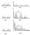
- Figures 1B, 2B and 3B show diffraction figures corresponding to the structures respectively shown in Figures 1A, 2A and 3A. There is a series of intense light spots on either side of the specular reflection spot (only one side of the diffraction pattern is shown in Figures 1B to 3B and only from order 6).
- the diffraction pattern changes continuously at the start of the etching of the metal layer 3.
- This diffraction pattern then changes very significantly when moving from a continuous layer 3 to residues scattered and then when one passes from the etching level corresponding to FIG. 2A to that corresponding to FIG. 3A, that is to say when one passes from a structure in which remain metal residues of very small dimensions, with a structure free of metallic residues.
- the invention therefore makes it possible to very sensitively detect the presence or absence of metal residues of very small dimensions, and this in an almost instantaneous manner, during the course of the etching operation.
- the light intensity measurement of one or more spots can be carried out using an analyzer moving along the diffraction pattern. It is also possible to carry out the measurement by sampling by means of a diode array.
- the liminous beam is for example obtained using a helium / neon type laser operating at a wavelength of 632.8 nm.
- the present invention can also be used for the control of engraved plates.
- the diffraction pattern obtained by lighting up a pattern of ribs 2 having been etched will be compared with diffraction patterns obtained previously during the calibration phases.
- This control process has the advantage of being precise, non-destructive and non-polluting.
- a diffraction grating has been previously described specially formed in an unused area of the substrate, one could use a pattern formed in a part of the circuit during manufacture, for example a memory area.
Landscapes
- Engineering & Computer Science (AREA)
- Physics & Mathematics (AREA)
- Manufacturing & Machinery (AREA)
- Plasma & Fusion (AREA)
- Chemical & Material Sciences (AREA)
- Power Engineering (AREA)
- Microelectronics & Electronic Packaging (AREA)
- Computer Hardware Design (AREA)
- Analytical Chemistry (AREA)
- General Physics & Mathematics (AREA)
- Condensed Matter Physics & Semiconductors (AREA)
- General Chemical & Material Sciences (AREA)
- Chemical Kinetics & Catalysis (AREA)
- Mechanical Engineering (AREA)
- Drying Of Semiconductors (AREA)
- Diffracting Gratings Or Hologram Optical Elements (AREA)
- Testing Or Measuring Of Semiconductors Or The Like (AREA)
- Investigating Materials By The Use Of Optical Means Adapted For Particular Applications (AREA)
Abstract
Description
La présente invention concerne un procédé permettant de détecter la fin d'attaque, et plus particulièrement l'élimination complète, d'une couche déposée sur un substrat. L'invention trouve des applications dans le domaine de la fabrication des circuits intégrés, en particulier afin de détecter la fin de l'attaque d'une couche mince métallique déposée sur un substrat présentant un certain relief.The present invention relates to a method for detecting the end of attack, and more particularly the complete removal, of a layer deposited on a substrate. The invention finds applications in the field of manufacturing integrated circuits, in particular for detecting the end of the attack of a thin metallic layer deposited on a substrate having a certain relief.
Dans un certain nombre d'opérations entrant dans la fabrication des circuits intégrés, on est amené à graver une couche métallique déposée sur une couche en matériau isolant. Il en est ainsi, par exemple, lors de la réalisation de plusieurs niveaux d'interconnection, au cours de laquelle on procède classiquement à la gravure des parties d'une couche métallique déposée sur une couche d'oxyde de silicium qui épouse les structures sous-jacentes et qui présente en conséquence un certain relief. On souhaite, dans ce cas, poursuivre une opération de gravure jusqu'à obtenir l'enlèvement complet de cette couche métallique dans certaines zones. Il faut cependant arrêter cette opération de gravure rapidement après cet enlèvement complet de la couche métallique, parce que la poursuite de cette gravure pourrait modifier ou altérer d'autres structures et en outre allongerait inutilement la durée de fabrication.In a number of operations involved in the manufacture of integrated circuits, it is necessary to etch a metal layer deposited on a layer of insulating material. This is so, for example, during the production of several interconnection levels, during which one conventionally proceeds to the etching of the parts of a metal layer deposited on a layer of silicon oxide which marries the structures under -jacent and which consequently presents a certain relief. In this case, it is desired to continue an etching operation until the complete removal of this metal layer in certain areas. However, this etching operation must be stopped quickly after this complete removal of the metallic layer, because the continuation of this etching could modify or alter other structures and would unnecessarily lengthen the manufacturing time.
Une difficulté réside dans le fait que, dans la phase finale de l'opération de gravure, la couche métallique ne subsiste que sous forme de résidus du métal de très faibles dimensions. Habituellement, ces résidus sont situés au voisinage des marches présentes dans la couche isolante sous-jacente. Etant donné que ces résidus ont de faibles dimensions, ils ne sont pas détectables par les systèmes classiques de détection de fin d'attaque. Pour être certain qu'aucun résidu ne subsistera après cette opération de gravure, on est donc amené classiquement à prolonger la durée de gravure de la couche métallique.One difficulty lies in the fact that, in the final phase of the etching operation, the metal layer only remains in the form of metal residues of very small dimensions. Usually, these residues are located in the vicinity of the steps present in the underlying insulating layer. Since these residues have small dimensions, they are not detectable by conventional end of attack detection systems. To be certain that no residue will remain after this etching operation, it is therefore conventionally required to extend the etching time of the metal layer.
Un objet de la présente invention est de prévoir un procédé de détermination précise de l'élimination complète d'une couche mince déposée sur un substrat.An object of the present invention is to provide a method for the precise determination of the complete elimination of a thin layer deposited on a substrate.
Un autre objet de la présente invention est de prévoir un tel procédé qui puisse être utilisé comme moyen de contrôle pour vérifier qu'une opération de gravure a été menée de façon satisfaisante.Another object of the present invention is to provide such a method which can be used as a means of control to verify that an etching operation has been carried out in a satisfactory manner.
Un autre objet de la présente invention est de prévoir un tel procédé qui puisse être mis en oeuvre in situ pendant une opération de gravure.Another object of the present invention is to provide such a method which can be implemented in situ during an etching operation.
Pour atteindre ces objets, l'invention prévoit un procédé de détermination de l'élimination complète d'une couche mince déposée sur un substrat, comprenant les étapes consistant à prévoir sur une zone de substrat un réseau de diffraction optique, la couche mince déposée sur le substrat recouvrant aussi ce réseau de diffraction, et l'attaque de la couche mince s'effectuant aussi au niveau de ce réseau de diffraction; éclairer le réseau par un faisceau lumineux monochromatique; et observer l'évolution de la lumière diffractée au cours de l'opération d'attaque de la couche mince, afin de déterminer l'instant où le matériau de la couche mince est intégralement ôté.To achieve these objects, the invention provides a method for determining the complete elimination of a thin layer deposited on a substrate, comprising the steps consisting in providing on an area of substrate an optical diffraction grating, the thin layer deposited on the substrate also covering this diffraction grating, and the attack of the thin layer also taking place at the level of this diffraction grating; illuminate the network with a monochromatic light beam; and observing the evolution of the diffracted light during the etching operation of the thin layer, in order to determine the instant when the material of the thin layer is completely removed.
Selon un mode de réalisation de la présente invention, la substrat correspond à une couche d'oxyde de silicium, le réseau de diffraction est obtenu par gravure anisotrope d'une zone déterminée de cette couche, et la couche mince est métallique.According to an embodiment of the present invention, the substrate corresponds to a layer of silicon oxide, the diffraction grating is obtained by anisotropic etching of a determined area of this layer, and the thin layer is metallic.
Selon un mode de réalisation de la présente invention, la figure de diffraction obtenue à partir du réseau est comparée à des figures de diffraction obtenues lors d'un étalonnage.According to an embodiment of the present invention, the diffraction pattern obtained from the grating is compared to diffraction patterns obtained during a calibration.
Ces objets, caractéristiques et avantages ainsi que d'autres de la présente invention seront illustrés plus en détail dans la description suivante de modes de réalisation particuliers faite en relation avec les figures jointes parmi lesquelles:
- la figure 1A représente schématiquement, en coupe transversale, une structure résultant de la mise en oeuvre du procédé selon l'invention, telle qu'elle apparaît lors d'une phase initiale de l'opération de gravure;
- la figure 1B représente une figure de diffraction correspondant à la structure de la figure 1A;
- les figures 2A et 2B correspondent respectivement aux figures 1A et 1B lors d'une phase intermédiaire de l'opération de gravure; et
- les figures 3A et 3B correspondent respectivement aux figures 1A et 1B lors de la phase finale de gravure.
- FIG. 1A schematically represents, in cross section, a structure resulting from the implementation of the method according to the invention, as it appears during an initial phase of the etching operation;
- FIG. 1B represents a diffraction figure corresponding to the structure of FIG. 1A;
- FIGS. 2A and 2B correspond respectively to FIGS. 1A and 1B during an intermediate phase of the etching operation; and
- Figures 3A and 3B correspond respectively to Figures 1A and 1B during the final etching phase.
Le procédé selon l'invention va être décrit dans le cas particulier de la gravure du deuxième niveau d'interconnexion d'un circuit intégré à plusieurs niveaux d'interconnexion. Il est toutefois clair que cela ne constitue qu'un exemple et que l'invention s'applique de façon générale à la détermination de l'élimination complète d'une couche mince.The method according to the invention will be described in the particular case of etching the second interconnection level of an integrated circuit with several interconnection levels. It is however clear that this is only an example and that the invention applies generally to the determination of the complete elimination of a thin layer.
Pour réaliser plusieurs niveaux d'interconnexion, on dépose une première couche métallique qui est gravée selon un motif de connexion choisi, puis une couche isolante, souvent en oxyde de silicium, dans laquelle on ménage des trous de passage. On dépose par dessurs la couche isolante une seconde couche métallique qui vient remplir les trous de passage. On effectue ensuite une gravure pleine plaque de cette seconde couche métallique afin d'enlever complètement le métal de cette couche présent sur la couche isolante sous-jacente, et en ne conservant du métal qu'à l'intérieur des trous de passage ménagés dans la couche isolant. Enfin on dépose une troisième couche métallique qui est gravée selon un motif de connexion choisi. L'opération de gravure de la seconde couche métallique est particulièrement délicate. En effet, cette gravure doit être prolongée assez longtemps pour qu'il n'y ait plus aucun résidu métallique sur la couche isolante, mais cette opération de gravure ne doit pas être prolongée au-delà pour éviter d'enlever trop de métal présent dans les trous de passage.To achieve several levels of interconnection, a first metal layer is deposited which is etched according to a chosen connection pattern, then an insulating layer, often made of silicon oxide, in which passage holes are provided. The insulating layer is deposited by a second metallic layer which fills the through holes. A second plate metal etching is then carried out in order to completely remove the metal from this layer present on the underlying insulating layer, and retaining metal only inside the through holes provided in the insulating layer. Finally, a third metal layer is deposited which is etched according to a chosen connection pattern. The etching operation of the second metal layer is particularly delicate. In fact, this etching must be prolonged long enough so that there is no longer any metallic residue on the insulating layer, but this etching operation must not be prolonged beyond to avoid removing too much metal present in through holes.
Comme cela est illustré en figure 1A, selon l'invention, dans le cas de la gravure de la seconde couche métallique, on dépose dans une zone inutilisée d'une plaquette en cours de traitement de couche isolante 1 constituant une partie de la couche isolante susmentionée. On forme dans cette zone un réseau de diffraction optique constitué d'un certain nombre de nervures équidistantes 2, 2′. La hauteur des nervures est du même ordre de grandeur que la hauteur des marches présentes sur le reste de la plaquette au niveau des circuits en cours de réalisation. La seconde couche métallique 3 recouvrant la couche isolante 1 recouvre également la zone comprenant le réseau de diffraction 2, 2′ et épouse le relief des nervures. La gravure de cette couche métallique 3 s'effectue dans la zone comprenant le réseau de diffraction en même temps que dans la zone utile.As illustrated in FIG. 1A, according to the invention, in the case of the etching of the second metal layer, an
La figure 2A représente la même structure lorsque l'opération de gravure de la couche métallique 3 est presque achevée. Des résidus 5 du métal de la couche 3 substistent, ces résidus se localisant principalement au pied des flancs verticaux du réseau de diffraction ou à leur voisinage. Ces résidus 5 peuvent présenter des formes diverses et ont des dimensions extrêmement faibles. Tant que subsistent de tels résidus 5, il convient de poursuivre l'opération de gravure, jusqu'à leur enlèvement complet, comme cela a été expliqué précédemment.FIG. 2A shows the same structure when the etching operation of the
La figure 3A représente la structure lorsque les résidus ont complètement disparu.FIG. 3A represents the structure when the residues have completely disappeared.
Selon un mode de mise en oeuvre de la présente invention, pendant l'opération de gravure de la couche 3, on éclaire le réseau de diffraction par un faisceau lumineux monochromatique et on observe l'évolution de la lumière diffractée.According to an embodiment of the present invention, during the etching operation of the
Les figures 1B, 2B et 3B représentent des figures de diffraction correspondant aux structures respectivement représentées en figures 1A, 2A et 3A. On observe une série de spots lumineux intenses de part et d'autre de la tache de réflexion spéculaire (un seul côté de la figure de diffraction est représenté sur les figures 1B à 3B et seulement à partir de l'ordre 6).Figures 1B, 2B and 3B show diffraction figures corresponding to the structures respectively shown in Figures 1A, 2A and 3A. There is a series of intense light spots on either side of the specular reflection spot (only one side of the diffraction pattern is shown in Figures 1B to 3B and only from order 6).
Les demandeurs remarqué que la figure de diffraction se modifie continûment au début de l'opération de gravure de la couche métallique 3. Cette figure de diffraction se modifie ensuite de façon très sensible lorsque l'on passe d'une couche 3 continue à des résidus épars et ensuite lorsque l'on passe du niveau de gravure correspondant à la figure 2A à celui correspondant à la figure 3A, c'est-à-dire lorsque l'on passe d'une structure dans laquelle subsistent des résidus de métal de très faibles dimensions, à une structure exempte de résidus métalliques. L'invention permet donc de détecter de façon très sensible la présence ou l'absence de résidus métalliques de très faibles dimensions, et cela d'une façon quasi-instantanée, pendant le déroulement de l'opération de gravure.Applicants have noticed that the diffraction pattern changes continuously at the start of the etching of the
Pour exploiter, de façon automatique, les modifications de la figure de diffraction, on peut étudier l'ensemble du spectre ou sélectionner dans cette figure de diffraction une seule tache ou un certain groupe G de taches de diffraction. L'intensité lumineuse de cette tache ou de ce groupe de taches varie dans de grandes proportions lorsque l'on passe d'une phase de gravure au cours de laquelle subsistent des résidus métalliques 5 à une phase finale de gravure pour laquelle les résidus métalliques ont été complètement éliminés. On peut alors aisément mesurer de façon automatique l'intensité lumineuse de ce groupe de taches afin de déterminer l'instant où les résidus métalliques 5 sont intégralement ôtés, cet instant étant défini par le passage par un seuil prédéterminé de la valeur de cette intensité lumineuse.To exploit, automatically, the modifications of the diffraction pattern, one can study the whole spectrum or select in this diffraction pattern a single spot or a certain group G of diffraction spots. The light intensity of this spot or of this group of spots varies in great proportions when one passes from an etching phase during which metal residues remain 5 to a final etching phase for which the residues have been completely eliminated. It is then easy to automatically measure the light intensity of this group of spots in order to determine the instant when the
On peut effectuer la mesure d'intensité lumineuse d'une ou de plusieurs taches à l'aide d'un analyseur se déplaçant le long de la figure de diffraction. On peut aussi effectuer la mesure par échantillonnage au moyen d'une barrette à diodes.The light intensity measurement of one or more spots can be carried out using an analyzer moving along the diffraction pattern. It is also possible to carry out the measurement by sampling by means of a diode array.
Le faisceau limineux est par exemple obtenu à l'aide d'un laser de type hélium/néon fonctionnant à une longueur d'onde de 632,8 nm.The liminous beam is for example obtained using a helium / neon type laser operating at a wavelength of 632.8 nm.
L'homme de l'art notera que, bien que l'invention ait été décrite en relation avec une application particulière, elle s'applique de façon générale à la détection de l'élimination complète d'une couche mince déposée sur un substrat massif ou sur une autre couche mince.Those skilled in the art will note that, although the invention has been described in relation to a particular application, it generally applies to the detection of the complete elimination of a thin layer deposited on a solid substrate or another thin layer.
D'autre part, on a décrit ci-dessous une mise en oeuvre in situ du procédé selon la présente invention dans laquelle le motif à tester est éclairé dans l'enceinte de gravure. La présente invention peut aussi être utilisée pour le contrôle de plaques gravées. En ce cas, on comparera la figure de diffraction obtenue en éclairant un motif de nervures 2 ayant subi une gravure à des figures de diffraction obtenues antérieurement au cours de phases d'étalonnage. Ce procédé de contrôle présente l'avantage d'être précis, non destructif et non polluant. Ainsi si l'on détecte qu'un lot de plaquettes a subi une gravure insuffisante, on pourra, sans inconvénient, le soumettre à une phase de gravure supplémentaire.On the other hand, an in situ implementation of the method according to the present invention has been described in which the pattern to be tested is illuminated in the etching enclosure. The present invention can also be used for the control of engraved plates. In this case, the diffraction pattern obtained by lighting up a pattern of
Alors que l'on a décrit précedemment un réseau de diffraction formé spécialement dans une zone inutilisée du substrat, on pourrait utiliser un motif formé dans une partie du circuit en cours de fabrication, par exemple une zone de mémoire.While a diffraction grating has been previously described specially formed in an unused area of the substrate, one could use a pattern formed in a part of the circuit during manufacture, for example a memory area.
Claims (6)
Applications Claiming Priority (2)
| Application Number | Priority Date | Filing Date | Title |
|---|---|---|---|
| FR9009467A FR2665024B1 (en) | 1990-07-20 | 1990-07-20 | METHOD FOR DETERMINING THE COMPLETE REMOVAL OF A THIN FILM FROM A NON-PLANAR SUBSTRATE. |
| FR9009467 | 1990-07-20 |
Publications (2)
| Publication Number | Publication Date |
|---|---|
| EP0468897A1 true EP0468897A1 (en) | 1992-01-29 |
| EP0468897B1 EP0468897B1 (en) | 1995-11-15 |
Family
ID=9399066
Family Applications (1)
| Application Number | Title | Priority Date | Filing Date |
|---|---|---|---|
| EP91420256A Expired - Lifetime EP0468897B1 (en) | 1990-07-20 | 1991-07-16 | Process for the determination of the complete removal of a thin film on a non-planar substrate |
Country Status (5)
| Country | Link |
|---|---|
| US (1) | US5186786A (en) |
| EP (1) | EP0468897B1 (en) |
| JP (1) | JPH06252103A (en) |
| DE (1) | DE69114595T2 (en) |
| FR (1) | FR2665024B1 (en) |
Cited By (13)
| Publication number | Priority date | Publication date | Assignee | Title |
|---|---|---|---|---|
| US5433651A (en) * | 1993-12-22 | 1995-07-18 | International Business Machines Corporation | In-situ endpoint detection and process monitoring method and apparatus for chemical-mechanical polishing |
| WO1996002807A1 (en) * | 1994-07-13 | 1996-02-01 | Leonhard Kurz Gmbh & Co. | Process for measuring the depth of a microstructure |
| US5964643A (en) * | 1995-03-28 | 1999-10-12 | Applied Materials, Inc. | Apparatus and method for in-situ monitoring of chemical mechanical polishing operations |
| US6524164B1 (en) | 1999-09-14 | 2003-02-25 | Applied Materials, Inc. | Polishing pad with transparent window having reduced window leakage for a chemical mechanical polishing apparatus |
| US6537133B1 (en) | 1995-03-28 | 2003-03-25 | Applied Materials, Inc. | Method for in-situ endpoint detection for chemical mechanical polishing operations |
| US6676717B1 (en) | 1995-03-28 | 2004-01-13 | Applied Materials Inc | Apparatus and method for in-situ endpoint detection for chemical mechanical polishing operations |
| US6716085B2 (en) | 2001-12-28 | 2004-04-06 | Applied Materials Inc. | Polishing pad with transparent window |
| US6719818B1 (en) | 1995-03-28 | 2004-04-13 | Applied Materials, Inc. | Apparatus and method for in-situ endpoint detection for chemical mechanical polishing operations |
| US6849152B2 (en) | 1992-12-28 | 2005-02-01 | Applied Materials, Inc. | In-situ real-time monitoring technique and apparatus for endpoint detection of thin films during chemical/mechanical polishing planarization |
| US6991517B2 (en) | 1999-02-04 | 2006-01-31 | Applied Materials Inc. | Linear polishing sheet with window |
| US6994607B2 (en) | 2001-12-28 | 2006-02-07 | Applied Materials, Inc. | Polishing pad with window |
| US7001242B2 (en) | 2002-02-06 | 2006-02-21 | Applied Materials, Inc. | Method and apparatus of eddy current monitoring for chemical mechanical polishing |
| US8795029B2 (en) | 1995-03-28 | 2014-08-05 | Applied Materials, Inc. | Apparatus and method for in-situ endpoint detection for semiconductor processing operations |
Families Citing this family (2)
| Publication number | Priority date | Publication date | Assignee | Title |
|---|---|---|---|---|
| US5395769A (en) * | 1992-06-26 | 1995-03-07 | International Business Machines Corporation | Method for controlling silicon etch depth |
| US7361584B2 (en) | 2004-11-04 | 2008-04-22 | International Business Machines Corporation | Detection of residual liner materials after polishing in damascene process |
Citations (3)
| Publication number | Priority date | Publication date | Assignee | Title |
|---|---|---|---|---|
| US4141780A (en) * | 1977-12-19 | 1979-02-27 | Rca Corporation | Optically monitoring the thickness of a depositing layer |
| EP0294873A1 (en) * | 1987-06-04 | 1988-12-14 | Laboratoires D'electronique Philips | Test apparatus for performing a realization process of semiconductor structures |
| US4840487A (en) * | 1985-06-19 | 1989-06-20 | Hitachi, Ltd. | Measuring apparatus for etching pits |
Family Cites Families (1)
| Publication number | Priority date | Publication date | Assignee | Title |
|---|---|---|---|---|
| US4680084A (en) * | 1984-08-21 | 1987-07-14 | American Telephone And Telegraph Company, At&T Bell Laboratories | Interferometric methods and apparatus for device fabrication |
-
1990
- 1990-07-20 FR FR9009467A patent/FR2665024B1/en not_active Expired - Fee Related
-
1991
- 1991-07-16 DE DE69114595T patent/DE69114595T2/en not_active Expired - Lifetime
- 1991-07-16 EP EP91420256A patent/EP0468897B1/en not_active Expired - Lifetime
- 1991-07-18 JP JP3177865A patent/JPH06252103A/en active Pending
- 1991-07-19 US US07/732,192 patent/US5186786A/en not_active Expired - Lifetime
Patent Citations (3)
| Publication number | Priority date | Publication date | Assignee | Title |
|---|---|---|---|---|
| US4141780A (en) * | 1977-12-19 | 1979-02-27 | Rca Corporation | Optically monitoring the thickness of a depositing layer |
| US4840487A (en) * | 1985-06-19 | 1989-06-20 | Hitachi, Ltd. | Measuring apparatus for etching pits |
| EP0294873A1 (en) * | 1987-06-04 | 1988-12-14 | Laboratoires D'electronique Philips | Test apparatus for performing a realization process of semiconductor structures |
Non-Patent Citations (2)
| Title |
|---|
| PROCEEDINGS OF THE SPIE, vol. 990, CHEMICAL, BIOCHEMICAL AND ENVIRONMENTAL APPLICATON OF FIBERS, 1988, pages 158-162; B. LALOUX et al.: Non-destructive testing of reflow on Si wafer" * |
| THIN SOLID FILMS, vol. 109, no. 4, 25 novembre 1983, pages 363-369; E.S. BRAGA et al.: "Optical monitoring of the end point in thin film plasma etching" * |
Cited By (22)
| Publication number | Priority date | Publication date | Assignee | Title |
|---|---|---|---|---|
| US6849152B2 (en) | 1992-12-28 | 2005-02-01 | Applied Materials, Inc. | In-situ real-time monitoring technique and apparatus for endpoint detection of thin films during chemical/mechanical polishing planarization |
| US7024063B2 (en) | 1992-12-28 | 2006-04-04 | Applied Materials Inc. | In-situ real-time monitoring technique and apparatus for endpoint detection of thin films during chemical/mechanical polishing planarization |
| US5433651A (en) * | 1993-12-22 | 1995-07-18 | International Business Machines Corporation | In-situ endpoint detection and process monitoring method and apparatus for chemical-mechanical polishing |
| WO1996002807A1 (en) * | 1994-07-13 | 1996-02-01 | Leonhard Kurz Gmbh & Co. | Process for measuring the depth of a microstructure |
| AU691622B2 (en) * | 1994-07-13 | 1998-05-21 | Leonhard Kurz Gmbh & Co. | Process for measuring the depth of a microstructure |
| US6860791B2 (en) | 1995-03-28 | 2005-03-01 | Applied Materials, Inc. | Polishing pad for in-situ endpoint detection |
| US8795029B2 (en) | 1995-03-28 | 2014-08-05 | Applied Materials, Inc. | Apparatus and method for in-situ endpoint detection for semiconductor processing operations |
| US6719818B1 (en) | 1995-03-28 | 2004-04-13 | Applied Materials, Inc. | Apparatus and method for in-situ endpoint detection for chemical mechanical polishing operations |
| US6537133B1 (en) | 1995-03-28 | 2003-03-25 | Applied Materials, Inc. | Method for in-situ endpoint detection for chemical mechanical polishing operations |
| US6875078B2 (en) | 1995-03-28 | 2005-04-05 | Applied Materials, Inc. | Apparatus and method for in-situ endpoint detection for chemical mechanical polishing operations |
| US6676717B1 (en) | 1995-03-28 | 2004-01-13 | Applied Materials Inc | Apparatus and method for in-situ endpoint detection for chemical mechanical polishing operations |
| US5964643A (en) * | 1995-03-28 | 1999-10-12 | Applied Materials, Inc. | Apparatus and method for in-situ monitoring of chemical mechanical polishing operations |
| US6991517B2 (en) | 1999-02-04 | 2006-01-31 | Applied Materials Inc. | Linear polishing sheet with window |
| US7189141B2 (en) | 1999-09-14 | 2007-03-13 | Applied Materials, Inc. | Polishing pad with transparent window having reduced window leakage for a chemical mechanical polishing apparatus |
| US6524164B1 (en) | 1999-09-14 | 2003-02-25 | Applied Materials, Inc. | Polishing pad with transparent window having reduced window leakage for a chemical mechanical polishing apparatus |
| US6896585B2 (en) | 1999-09-14 | 2005-05-24 | Applied Materials, Inc. | Polishing pad with transparent window having reduced window leakage for a chemical mechanical polishing apparatus |
| US7677959B2 (en) | 1999-09-14 | 2010-03-16 | Applied Materials, Inc. | Multilayer polishing pad and method of making |
| US6994607B2 (en) | 2001-12-28 | 2006-02-07 | Applied Materials, Inc. | Polishing pad with window |
| US7198544B2 (en) | 2001-12-28 | 2007-04-03 | Applied Materials, Inc. | Polishing pad with window |
| US6716085B2 (en) | 2001-12-28 | 2004-04-06 | Applied Materials Inc. | Polishing pad with transparent window |
| US7591708B2 (en) | 2002-02-06 | 2009-09-22 | Applied Materials, Inc. | Method and apparatus of eddy current monitoring for chemical mechanical polishing |
| US7001242B2 (en) | 2002-02-06 | 2006-02-21 | Applied Materials, Inc. | Method and apparatus of eddy current monitoring for chemical mechanical polishing |
Also Published As
| Publication number | Publication date |
|---|---|
| FR2665024B1 (en) | 1994-02-18 |
| FR2665024A1 (en) | 1992-01-24 |
| US5186786A (en) | 1993-02-16 |
| EP0468897B1 (en) | 1995-11-15 |
| DE69114595T2 (en) | 1996-05-02 |
| DE69114595D1 (en) | 1995-12-21 |
| JPH06252103A (en) | 1994-09-09 |
Similar Documents
| Publication | Publication Date | Title |
|---|---|---|
| EP0468897B1 (en) | Process for the determination of the complete removal of a thin film on a non-planar substrate | |
| EP2917688B1 (en) | Method for measuring thickness variations in a layer of a multilayer semiconductor structure | |
| EP3077873B1 (en) | Device and method for positioning a photolithography mask by means of a contactless optical method | |
| EP1364181B1 (en) | Method and device for high-speed interferential microscopic imaging of an object | |
| FR3026481A1 (en) | DEVICE AND METHOD FOR SURFACE PROFILOMETRY FOR CONTROLLING WAFERS DURING PROCESS | |
| CN108225195A (en) | Non-destructive testing cutting tip is in the method for determining coating layer thickness | |
| EP3836214B1 (en) | Light sensor | |
| EP0294873A1 (en) | Test apparatus for performing a realization process of semiconductor structures | |
| US6885446B2 (en) | Method and system for monitoring a process of material removal from the surface of a patterned structure | |
| KR100502120B1 (en) | Method of judging residual film by optical measurement | |
| KR100684102B1 (en) | Method of inspecting a defect and apparatus for inspecting a defect using the same | |
| EP0446549B1 (en) | Procedure to measure the dimensions of a spacer | |
| FR3062516A1 (en) | METHOD OF MEASURING THE DEALIGNMENT BETWEEN A FIRST AND A SECOND GRATING AREA | |
| EP0274966B1 (en) | Process for the quantitative determination of the shape of relief patterns having very small dimensions | |
| FR2742871A1 (en) | Semiconductor circuit metal layer defect locating method | |
| JP2001221617A (en) | Method of measuring step, method of manufacturing stamper, stamper, method of manufacturing optical disk, optical disk, method of manufacturing semiconductor device, semiconductor device, and step measuring instrument | |
| EP0378033A1 (en) | Process for setting up a photolithographic exposure machine | |
| JP3681319B2 (en) | Film thickness measuring method and apparatus | |
| EP3749919B1 (en) | Method and device for inspecting a surface of an object comprising non-similar materials | |
| FR3030032A1 (en) | METHOD FOR DETERMINING THE THICKNESS OF A THIN LAYER BY MULTI-WAVELENGTH INTERFEROMETRY, COMPUTER PROGRAM PRODUCT, STORAGE MEDIUM AND SYSTEM THEREOF | |
| FR2551210A1 (en) | METHOD OF CONTROLLING A NETWORK | |
| FR2537321A1 (en) | IMPROVEMENTS IN THE MANUFACTURE OF MAGNETIC BUBBLE DEVICES | |
| KR102053886B1 (en) | Sample analysis method using spectroscopic reflectometry | |
| EP0262055A1 (en) | Flow-measuring process | |
| FR2598508A1 (en) | Method and apparatus for determining the end of attack of an etched surface |
Legal Events
| Date | Code | Title | Description |
|---|---|---|---|
| PUAI | Public reference made under article 153(3) epc to a published international application that has entered the european phase |
Free format text: ORIGINAL CODE: 0009012 |
|
| AK | Designated contracting states |
Kind code of ref document: A1 Designated state(s): DE FR GB IT |
|
| 17P | Request for examination filed |
Effective date: 19920703 |
|
| 17Q | First examination report despatched |
Effective date: 19950131 |
|
| GRAA | (expected) grant |
Free format text: ORIGINAL CODE: 0009210 |
|
| AK | Designated contracting states |
Kind code of ref document: B1 Designated state(s): DE FR GB IT |
|
| GBT | Gb: translation of ep patent filed (gb section 77(6)(a)/1977) |
Effective date: 19951120 |
|
| REF | Corresponds to: |
Ref document number: 69114595 Country of ref document: DE Date of ref document: 19951221 |
|
| ITF | It: translation for a ep patent filed | ||
| PLBE | No opposition filed within time limit |
Free format text: ORIGINAL CODE: 0009261 |
|
| STAA | Information on the status of an ep patent application or granted ep patent |
Free format text: STATUS: NO OPPOSITION FILED WITHIN TIME LIMIT |
|
| 26N | No opposition filed | ||
| REG | Reference to a national code |
Ref country code: GB Ref legal event code: IF02 |
|
| PGFP | Annual fee paid to national office [announced via postgrant information from national office to epo] |
Ref country code: IT Payment date: 20080717 Year of fee payment: 18 |
|
| REG | Reference to a national code |
Ref country code: GB Ref legal event code: 732E Free format text: REGISTERED BETWEEN 20090924 AND 20090930 |
|
| PGFP | Annual fee paid to national office [announced via postgrant information from national office to epo] |
Ref country code: DE Payment date: 20100730 Year of fee payment: 20 Ref country code: FR Payment date: 20100813 Year of fee payment: 20 Ref country code: GB Payment date: 20100616 Year of fee payment: 20 |
|
| PG25 | Lapsed in a contracting state [announced via postgrant information from national office to epo] |
Ref country code: IT Free format text: LAPSE BECAUSE OF NON-PAYMENT OF DUE FEES Effective date: 20090716 |
|
| REG | Reference to a national code |
Ref country code: DE Ref legal event code: R071 Ref document number: 69114595 Country of ref document: DE |
|
| REG | Reference to a national code |
Ref country code: DE Ref legal event code: R071 Ref document number: 69114595 Country of ref document: DE |
|
| REG | Reference to a national code |
Ref country code: GB Ref legal event code: PE20 Expiry date: 20110715 |
|
| PG25 | Lapsed in a contracting state [announced via postgrant information from national office to epo] |
Ref country code: GB Free format text: LAPSE BECAUSE OF EXPIRATION OF PROTECTION Effective date: 20110715 |
|
| PG25 | Lapsed in a contracting state [announced via postgrant information from national office to epo] |
Ref country code: DE Free format text: LAPSE BECAUSE OF EXPIRATION OF PROTECTION Effective date: 20110717 |