EP0468521A2 - Method and apparatus for irradiating low-energy electrons - Google Patents
Method and apparatus for irradiating low-energy electrons Download PDFInfo
- Publication number
- EP0468521A2 EP0468521A2 EP91112602A EP91112602A EP0468521A2 EP 0468521 A2 EP0468521 A2 EP 0468521A2 EP 91112602 A EP91112602 A EP 91112602A EP 91112602 A EP91112602 A EP 91112602A EP 0468521 A2 EP0468521 A2 EP 0468521A2
- Authority
- EP
- European Patent Office
- Prior art keywords
- energy
- electron beam
- low
- irradiating
- electrons
- Prior art date
- Legal status (The legal status is an assumption and is not a legal conclusion. Google has not performed a legal analysis and makes no representation as to the accuracy of the status listed.)
- Granted
Links
Images


Classifications
-
- H—ELECTRICITY
- H01—ELECTRIC ELEMENTS
- H01J—ELECTRIC DISCHARGE TUBES OR DISCHARGE LAMPS
- H01J37/00—Discharge tubes with provision for introducing objects or material to be exposed to the discharge, e.g. for the purpose of examination or processing thereof
- H01J37/02—Details
- H01J37/04—Arrangements of electrodes and associated parts for generating or controlling the discharge, e.g. electron-optical arrangement, ion-optical arrangement
- H01J37/05—Electron or ion-optical arrangements for separating electrons or ions according to their energy or mass
-
- H—ELECTRICITY
- H01—ELECTRIC ELEMENTS
- H01J—ELECTRIC DISCHARGE TUBES OR DISCHARGE LAMPS
- H01J37/00—Discharge tubes with provision for introducing objects or material to be exposed to the discharge, e.g. for the purpose of examination or processing thereof
- H01J37/02—Details
- H01J37/026—Means for avoiding or neutralising unwanted electrical charges on tube components
-
- H—ELECTRICITY
- H01—ELECTRIC ELEMENTS
- H01J—ELECTRIC DISCHARGE TUBES OR DISCHARGE LAMPS
- H01J37/00—Discharge tubes with provision for introducing objects or material to be exposed to the discharge, e.g. for the purpose of examination or processing thereof
- H01J37/02—Details
- H01J37/04—Arrangements of electrodes and associated parts for generating or controlling the discharge, e.g. electron-optical arrangement, ion-optical arrangement
- H01J37/06—Electron sources; Electron guns
- H01J37/073—Electron guns using field emission, photo emission, or secondary emission electron sources
Definitions
- the present invention relates to a method and apparatus for irradiating low-energy electrons, and in particular to a method of forming a low-energy electron beam used in a process such as neutralization of a charged status created by processing a semiconductor wafer, conversion of positive ions into negative ions in order to process a surface of a semiconductor substrate.
- a charged beam apparatus irradiates ions or an electron beam onto an insulated sample such as a semiconductor wafer or a non-grounded floating sample (hereinafter simply called “sample”), to either enable analysis using secondary electrons or secondary ions emitted from the sample's surface, or to use the ion beam for ion implantation or ion etching of the semiconductor wafer's surface.
- a positive ion beam is irradiated onto the sample, the sample builds up a positive charge from the incident positive ions or the secondary electrons generated by the ion beam irradiation.
- This positive charging of the sample causes various problems in the use of ion beam devices.
- One example of a problem caused if the ion beam device is used for mass spectroscopy is described below.
- SIMS Secondary ion mass spectroscopy
- charge on the sample's surface caused by the above described positive ion beam irradiation will change the positiveness of the sample's voltage, and/or generate an electric field in the vicinity of the surface of the sample. Changes in the energy distribution of the secondary ions caused by this charge will reduce the transmissivity of the energy distribution, and thus reduce the detection efficiency. Charge on the sample is a major cause of variations in detection efficiency in SIMS.
- Another example of the problems occurs when the ion beam irradiation apparatus is used for semiconductor devices.
- An ion implantation apparatus that irradiates a large-current ion beam at the semiconductor devices is used, but if the charge on the semiconductor wafer is too large, the insulation will break down and the semiconductor devices will be damaged.
- an ion beam etching apparatus that maintains an ion source at a positive charge, generates a plasma using an inert gas, and draws inert gas ions from the ion source to irradiate them onto a wafer to etch the surface of the wafer; an ion beam sputtering device that draws out an ion beam accelerated at a high energy level from an independent ion source and bombards it onto a target placed in high-vacuum atmosphere, to form a layer on a sample such as a semiconductor wafer in a low-pressure gas at 0.01 Pa or less; an ion plating device that ionizes or activates vaporized atoms from a vaporization source activated by a glow discharge to accelerate them, then bombards them onto a semiconductor wafer placed on a cathode side to form a thin layer thereon by deposition; or a cluster ion beam deposition device that ionizes a cluster of 100 to 1000 atoms in
- FIG. 9 A conventional method of electron beam irradiation using this form of charge neutralization is illustrated in Fig. 9.
- an ion beam 901 having a positive charge is irradiated onto a wafer 902 by an ion beam apparatus (not shown in the figure).
- Either the ion beam itself, or the beam of secondary electrons generated by the ion beam positively charges the irradiated surface.
- This portion is a charged portion 909.
- Electrons 905 are irradiated onto the sample's surface in order to neutralize the charged portion 909.
- a power source V F 906 applies a voltage to a cathode 903 to heat it.
- the electrons 905 emitted from the cathode 903 are accelerated by an acceleration voltage from a voltage source V A 908 applied between the cathode 903 and the wafer 902, and are irradiated onto the charged portion 909 on the water 902.
- a reflection plate 904 is provided around the cathode 903 to suppress scattering of the electrons 905 and direct them, and a voltage source V R 907 is connected between this reflection plate 904 and the cathode 903 to negatively bias the reflection plate 904 with respect to the cathode, and thus the positive charge on the charged portion 909 is neutralized by the electrons 905.
- neutral activated species or positive ions are used.
- RIE reactive ion etching
- a reactive gas plasma is formed by high-frequency discharge, a water surface is exposed to this plasma so that a self-bias voltage (Vdc) is induced in the surface, positive cons are drawn out from the plasma, and active species that have been adsorbed into the wafer surface are bombarded by the ions to etch the surface.
- Vdc self-bias voltage
- the ion energy is usually at least 100 eV, and it could even be several 100 eV.
- the LOCOS method is usually used.
- a mask pattern of a substance such as a nitride film is formed on the wafer surface and the wafer is exposed in an oxidizing atmosphere so that a thick oxide film forms on the parts of the wafer surface not covered by the mask.
- the oxide film is eaten away by a phenomenon called bird's beaks at the boundary between the wafer and the mask material, so the oxide portions must be made unnecessarily large, destroying the high levels of integration.
- Recent thinking has suggested using negative ions such as NF 3 - ions to improve selectivity in this etching.
- negative ions such as NF 3 - ions to improve selectivity in this etching.
- atoms or molecules of a reactive gas are given a negative charge, and the semiconductor substrate being processed, such as a wafer, is exposed to these ions.
- a material that tends to form chemical bonds with the negative ions of the reactive gas such as a silicon oxide film, has a far greater adsorption that a material that does not have this tendency, such as silicon, so that the adsorbency efficiency of the etching species is greater and therefore the etching speed is relatively higher.
- This enables highly selective etching of substances such as oxide films, and also the use of negative oxygen ions during the formation of oxide films.
- a silicon semiconductor substrate can be heated to approximately 800 C, and a bias voltage of about 10 V can be applied to draw out negative ions.
- a silicon oxide film can be formed on a substrate in this state by placing it into an atmosphere of negative oxygen ions.
- the negative oxygen ions drawn to the boundary formed by the bias voltage are diffused in the lengthwise direction on the semiconductor substrate, so the oxide can be given directionality, thus reducing bird's beaks.
- the diffusion that occurs in impurity diffusion processing can be given directionality by forming the above oxide film by turning atoms of an impurity such as phosphorus, boron, or arsenic into negative ions, then heating the semiconductor substrate while a bias voltage is applied to it.
- the hot electrons 905 accelerated by the voltage source V A 908 are irradiated onto the wafer.
- the voltage of the voltage source V A 908 is normally set to between -100 V to -500 V. If electrons of an energy of 100 eV or greater are irradiated onto the wafer, excess electrons will be supplied and the potential of the wafer surface will drop to negative. This drop in the potential of the sample's surface will shift the energy distribution of the secondary ions (positive ions) emitted from the sample's surface toward the low-energy side, by an amount equal to the surface potential. The shift will be toward the high-energy side for negative secondary ions or secondary electrons.
- a method is known of selectively irradiating low-energy electrons onto the charged portion in order to remove the supply of excess electrons (Japanese Patent Laid Open No. 63-257175 (1988)-).
- Japanese Patent Laid Open No. 63-257175 (1988)- Japanese Patent Laid Open No. 63-257175 (1988)-.
- negative ions that can etch both efficiently and selectively can be formed by irradiating radical ions of low-energy electrons, but it is extremely difficult to efficiently control this energy.
- the negative ions are formed by introducing a gas such as NF 3 , CIF 3 , Cb, or F 2 into a discharge tube, then cracking it with some means such as microwave discharge. After the cracking, the atoms such as fluorine or chlorine that are reactive gas components generated by the cracking are supplied to a vacuum chamber. When these atoms are irradiated by a low-energy electron beam, negative ions of fluorine or chlorine are formed.
- the energy of the electron beam used to negatively ionize these atoms is set to be maintained lower than the energy needed to ionize the atoms, so that no positive ions are generated. This value is approximately 10 to 15 eV, regardless of the atoms, which means that if the energy of the electron beam used to negatively ionize the atoms is held to below about 20 eV, the amount of positive ions generated can be kept extremely low. Even when the reactive gas is in molecule state, the necessary energy is virtually the same as that for atoms. Creating the low-energy electron beam necessary for this negative ionization is difficult, and controlling this energy is also a problem.
- An objective of the present invention to provide a method of irradiating a low-energy beam that can provide good control in the irradiation of a low-energy beam that has no energy components above a certain value, and an irradiation device that uses this method.
- a method of irradiating low-energy electrons comprising the steps of irradiating a primary electron beam from a primary electron beam irradiation portion onto a secondary electron emission portion to emit a secondary electron beam; accelerating the emitted secondary electron beam; removing high-energy components from the accelerated secondary beam; and decelerating the secondary electron beam without the high-energy components into a focus.
- an apparatus for irradiating low-energy electrons comprising: means for irradiating a primary electron beam; means for emitting a secondary electron, the means receiving a primary electron beam generated from the means for irradiating a primary electron beam and emitting a secondary electron beam; means for accelerating the secondary electron beam; energy analyzing means which removes high-energy components from the accelerated secondary electron beam, to obtain low-energy secondary electrons; and deceleration means for decelerating the low-energy secondary electrons into a focus.
- low-energy electrons having an emission velocity or required energy components of a narrow energy distribution can be controlled extremely easily by accelerating secondary electrons emitted from a target of a secondary electron emission portion, passing them through an energy analyzer portion where high-energy components are removed, then passing them through a deceleration device to focus them.
- a primary electron beam irradiation section comprises a cathode 101, an anode 103, and einzel lenses 104, 105, and 106.
- the cathode 101 is made of tungsten.
- a reflection plate 102 is provided in such a manner as to surround the cathode 101 and control the scattering of electrons generated from the cathode.
- the cathode 101 is heated by a heating power source V F 116 that has an output voltage of 44 V and a current of 0 to 7 A.
- a bias voltage source V R 117 that negatively biases the reflection plate 102 with respect to the cathode 101 is set to an output voltage of 0 to 50 V.
- An acceleration voltage power source V A 218 that generates an acceleration voltage applied between the cathode 101 and the anode 103 has an output voltage of 0 to 800 V.
- the anode 103 is grounded.
- a point between the electrostatic einzel lenses 104 and 106 is grounded, and a negative voltage of 0 to 800 V is applied to the center electrode 105 by a power source 119.
- a primary electron beam emitted from the primary electron beam irradiation section of this structure is accelerated, and is irradiated upon a target surface of a secondary electron emission section 107.
- a bias application power source 120 is connected to the secondary electron emission portion 107, and a bias voltage V T set to 0 to -20 V is applied thereto.
- a grounded shielding electrode 108 is provided in the vicinity of the secondary electron emission section 107, together with a draw-out electrode 109.
- a voltage of 0 to 200 V is applied to the draw-out electrode 109 by a voltage application power source 121.
- the electron beam is accelerated by the difference between the voltage applied to the secondary electron emission portion 107 and that applied to the draw-out electrode 109, and is sent on to an energy distribution section.
- Parallel flat-plate energy analyzers 110 and 111 are provided behind the draw-out electrode 109, and each flat plate receives an output voltage of 0 to 40 V from power sources 123 and 122.
- the energy analysis section provided in this way in the vicinity of the secondary electron emission section 107 receives secondary electrons emitted from the secondary electron emission section 107 and is used to remove high-energy components therefrom.
- This analysis portion comprises the shielding electrode 108, the draw-out electrode 109, and the parallel flat-plate energy analyzers 110 and 111. Electrodes 112 and 113 are provided behind this analysis portion to create a chargeless region, and the same output voltage in the range of 0 to 100 V is applied to both electrodes from a power source 124. Deceleration electrodes 114 and 115 are provided behind the electrodes 112 and 113. An output voltage of 0 to 40 V is applied to the electrode 114 from a power source 125, and the electrode 115 is grounded.
- the deceleration lens assembly provided as means of decelerating and focusing the low-energy electrons comprises the electrodes 112 and 113 and the deceleration electrodes 114 and 115.
- metal is used as the material of the irradiation surface of the secondary electron emission section 107, in other words, as the target.
- the emission efficiency can be increased.
- the irradiation angle 0 of the primary beam is 40 ⁇ .
- the secondary electrons emitted from the secondary electron emission section 107 are accelerated by the voltage V T from the bias application power source 120 or the voltage from the voltage application power source 121, and are extracted into an energy distribution section by the electric field of the extraction electrode 109.
- a voltage of -10 V is applied in the secondary electron emission section 107, and a voltage of +200 V is applied in the extraction electrode 109.
- the shielding electrode 108 is used to adjust the field distribution at the end portion of the extraction electrode 109, to relieve the field.
- the high-energy components of the accelerated secondary electrons are removed by the parallel flat-plate energy analyzers 110 and 111.
- high-energy reflection primary electrons or high-energy secondary electrons proceed in a direction (A) in Fig. 1, whereas low-energy secondary electrons (B) are bent by the electrodes 110 and 111 to pass through the slit of the electrode 112.
- + 10 V is applied to the electrode 110
- + 190 V is applied to the electrode 111.
- the high-energy components are removed and only the low-energy secondary electrons pass through the slit of the electrode 112 and are incident into the drift region formed by the electrodes 112 and 113. This region is provided to enable adjustment of the introduction to the deceleration electrodes 114 and 115.
- a voltage of +70 V is applied to each of the electrodes 112 and 113.
- the secondary electrons that have passed through the drift region are decelerated by the deceleration electrodes 114 and 115.
- a voltage of 20 V is applied to the electrode 114, and the electrode 115 is grounded.
- the focal distance at this focus is controlled by the electrode 114, and the decelerated low-energy electrons (at 20 eV or less) are emitted from the electrode 115.
- the irradiating apparatus of the present invention uses the energy filters 110 and 111 formed of energy analyzers to remove high-energy components or reflected electrons from the secondary electrons generated by the secondary electron emission section 107, and can provide a narrow electron energy distribution width, ensuring that only low-energy electrons off a comparatively uniform energy distribution are supplied thereby.
- a material that increases the secondary electron emission efficiency 6 can be selected for the target of the secondary electron emission portion 107, and a quantity of secondary electrons that is several times the primary electron beam current can be emitted by making the primary electrons incident at an angle on the target.
- the transmissivity 11 of the beam emitted toward a subsequent stage from the extraction electrode 109 can be increased by tightening the diameter of the primary electron beam. In this way, a large quantity of low-energy electrons can be supplied to the sample.
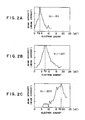
- Figs. 2A to 2C Energy distributions obtained when low-energy electrons were irradiated onto a sample using the device of the present invention are shown in Figs. 2A to 2C.
- the beam intensity (beam current) is plotted along the vertical axis and electron energy (eV) is plotted along the horizontal axis, with the peak value of electron energy distribution being Ep.
- These graphs show changes in energy distribution of electrons when they were irradiated with a voltage V T of -5 V (Fig. 2A), -10 V (Fig. 2B), and -20 V (Fig. 2C), from the power source 120 that applies a potential to the secondary electron emission portion 107. It can be clearly seen from these figures that as the voltage V T becomes more negative, the energy distribution shifts toward the high-energy side.
- the amount of the shift more-or-less agrees with the voltage V T applied to the secondary electron emission section 107. This is considered to be due to a high-energy offset imposed by the secondary electron emission voltage V T on the energy distribution of the secondary electrons generated by the secondary electron emission section 107.
- FIG. 3 The relationship between this target voltage V T and peak energy position Ep in the electron energy distributions plotted in Figs. 2A to 2C is shown in Fig. 3.
- This figure shows that the energy distribution of the low-energy electron beam can be varied by varying the target voltage V T .
- the energy of the low-energy electron beam could be controlled by varying the voltage V T that accelerates the electrons, but the energy can also be controlled by changing the voltage of the deceleration electrodes.
- the energy of the electron beam can be controlled by varying both the voltage V T and the deceleration voltage at the same time.
- the emission efficiency 6 of the secondary electrons from the target depends on the angle 0 at which the primary electron beam irradiates the target.
- the primary electrons are incident on the target of the secondary electron emission section 107 at an angle 0 (the angle from the perpendicular to the target surface), as shown in Fig. 4.
- This irradiation angle 0 is defined as being equal to the angle of the target with respect to the optical axis of the primary electron beam, and, since the optical axis of the primary electron beam and the energy filters 110 and 111 of the energy analysis portion are arranged in parallel, this is equal to the angle of the target with respect to the energy filters.
- the secondary electrons When the primary electrons are incident on a position 107 on the target surface, the secondary electrons are emitted from that position and are scattered in a spherical shape centered on that position. In other words, regardless of the direction in which electron is emitted from the emission surface, the secondary electrons are emitted in accordance with the cosine emission side so that they are in proportion to the cosine of the angle that is normal to that surface.
- a characteristic graph showing how the transmissivity of the secondary electrons varies with change in the irradiation angle 0 is shown in Fig.
- the electron beam emitted from the low-energy electron irradiating apparatus described above is used in a variety of applications, such as for neutralizing a sample in a charged state, or for irradiating into a reactive gas to create negative ions.
- the irradiation apparatus using the low-energy irradiation method of the present invention can be used as an attachment beside an ion beam system that uses a process such as ion implantation, etching, or SIMS. If it is used as a neutralization device for charged portions in an ion implantation device, it is placed in such a manner that the electron beam strikes at somewhat of an angle to the charged portion, in the same way as in the conventional apparatus, as shown in Fig. 9.
- the ion beam system is an etching apparatus that etches the surface of a silicon or other semiconductor substrate 602, and a negative ion generation device 610 is provided therebeside.
- the etching apparatus is provided with a vacuum chamber 601 in the middle of which is mounted a susceptor 603 that supports a semiconductor substrate 602 of a substance such as silicon.
- the susceptor 603 can be temperature-controlled, or a DC voltage can be applied thereto.
- the vacuum chamber is provided with an entrance port 604 and an exit port 605 for a reactive gas.
- the entrance port 604 is connected to a discharge tube 606, for instance, and the reactive gas introduced therethrough, such as NF 3 at about 0.1 Torr, is activated by the discharge of microwaves 607 (200 W).
- the F atoms of the gas disassociated in the way are sent into the vacuum chamber 601.
- the end of the discharge tube 606 is provided with an orifice that maintains a pressure difference between the discharge tube and the vacuum chamber.
- a low-energy electron beam 609 emitted from the nearby negative ion formation device 610 is also introduced into the vacuum chamber 601. This electron beam 609 strikes the F atoms introduced into the vacuum chamber 601 to form F- ions that are used to etch the surface of the substrate 602.
- the electron beam can be supplied over the entire surface of the substrate 602 by moving the susceptor 603 backward and forward. If the energy of the electron beam can be kept lower than the ionization energy of the component atoms (17.4 eV for F atoms), no positive ions will be formed. Therefore if this energy is below about 20 eV, the formation of positive ions is extremely small, causing no problems.
- This etching device supplies F- ions from above the substrate 602, but the electron beam 609 from the negative ion formation device irradiates the F atoms parallel to the surface of the substrate 602, to form negative ions.
- an electric field E is generated by a voltage applied to the substrate, as shown in the figure, and a magnetic field B is generated perpendicular to the electric field E by a magnetic field generation device (not shown in the figure).
- the F atoms radicals
- this use of the electric field ensures that the F- ions are incident on the substrate 602 with good directionality.
- F ions generated as a side effect move in the opposite direction to the substrate and are not incident on the substrate. Since the F- ions are heavy, the effect of the combined E x B fields ensures that their paths change very little as they are incident on the substrate 602, but the lighter electrons are bent by the E x B fields and do not hit the substrate.
- the substrates to be processed are not limited to those where oxide films are formed on silicon substrate surfaces.
- This method can also be applied to the selective etching of a material having ionicity linkages, such as alumina or a nitride film, with respect to a material having neutral linkages, such as a semiconductor or metal.
- a gas containing a halogen, such as NF 3 , CIF 3 , Cb, F 2 , or SF 6 , or a gas that reacts readily with oxygen, such as CF 4 , CCI 4 , or CBrF 3 can be used as the reactive gas.
- the negative ion formation device of the present invention need not only be an etching device --it can also be an attachment to an oxidation device that forms an Si0 2 film on the surface of a silicon semiconductor substrate by oxidation, or an ion implantation device that implants an impurity into a semiconductor substrate. Since it operates with negative ions such as oxygen or arsenic, it can form an oxide film or a diffusion layer with good directionality.
- the irradiation method of the present invention provides an extremely effective irradiation device of the present invention that can accurately control the energy distribution of electrons that are irradiated.
- the material of the target is selected from substances which do not form oxides easily or which have a good secondary electron emission efficiency, such as gold, platinum, or tungsten.
- the material of the cathode is tungsten or LaB 6 .
- parallel flat-plate energy analyzers were used as the energy analysis means, but a cylindrical mirror analyzer such as that shown in Fig. 7 or a sector magnetic field analyzer such as that shown in Fig. 8 could also be used.
Landscapes
- Chemical & Material Sciences (AREA)
- Analytical Chemistry (AREA)
- Analysing Materials By The Use Of Radiation (AREA)
- Physical Or Chemical Processes And Apparatus (AREA)
Abstract
Description
- The present invention relates to a method and apparatus for irradiating low-energy electrons, and in particular to a method of forming a low-energy electron beam used in a process such as neutralization of a charged status created by processing a semiconductor wafer, conversion of positive ions into negative ions in order to process a surface of a semiconductor substrate. In general, a charged beam apparatus irradiates ions or an electron beam onto an insulated sample such as a semiconductor wafer or a non-grounded floating sample (hereinafter simply called "sample"), to either enable analysis using secondary electrons or secondary ions emitted from the sample's surface, or to use the ion beam for ion implantation or ion etching of the semiconductor wafer's surface. If a positive ion beam is irradiated onto the sample, the sample builds up a positive charge from the incident positive ions or the secondary electrons generated by the ion beam irradiation. This positive charging of the sample causes various problems in the use of ion beam devices. One example of a problem caused if the ion beam device is used for mass spectroscopy is described below.
- Secondary ion mass spectroscopy (SIMS) uses a method by which, in a pre-step of the mass spectroscopy, the energy of secondary ions is analyzed and only secondary ions of a certain energy level are subjected to the mass spectroscopy, in order to ensure highly accurate mass spectroscopy. However, charge on the sample's surface caused by the above described positive ion beam irradiation will change the positiveness of the sample's voltage, and/or generate an electric field in the vicinity of the surface of the sample. Changes in the energy distribution of the secondary ions caused by this charge will reduce the transmissivity of the energy distribution, and thus reduce the detection efficiency. Charge on the sample is a major cause of variations in detection efficiency in SIMS.
- Another example of the problems occurs when the ion beam irradiation apparatus is used for semiconductor devices. An ion implantation apparatus that irradiates a large-current ion beam at the semiconductor devices is used, but if the charge on the semiconductor wafer is too large, the insulation will break down and the semiconductor devices will be damaged.
- Similar problems occur with an ion beam etching apparatus that maintains an ion source at a positive charge, generates a plasma using an inert gas, and draws inert gas ions from the ion source to irradiate them onto a wafer to etch the surface of the wafer; an ion beam sputtering device that draws out an ion beam accelerated at a high energy level from an independent ion source and bombards it onto a target placed in high-vacuum atmosphere, to form a layer on a sample such as a semiconductor wafer in a low-pressure gas at 0.01 Pa or less; an ion plating device that ionizes or activates vaporized atoms from a vaporization source activated by a glow discharge to accelerate them, then bombards them onto a semiconductor wafer placed on a cathode side to form a thin layer thereon by deposition; or a cluster ion beam deposition device that ionizes a cluster of 100 to 1000 atoms in a hard vacuum, accelerates the cluster, and bombards it onto a wafer to form a thin layer by deposition. After one of these devices has been used, the sample such as a semiconductor wafer is charged, and the same insulation damage as that described above can occur.
- For this reason, when an ion beam device is used, it has become necessary to use a method designed to neutralize the charge by additionally irradiating a negatively charged electron beam onto the charged sample surface, in order to relieve the positive charge on the sample's surface.
- A conventional method of electron beam irradiation using this form of charge neutralization is illustrated in Fig. 9. First, an
ion beam 901 having a positive charge is irradiated onto awafer 902 by an ion beam apparatus (not shown in the figure). Either the ion beam itself, or the beam of secondary electrons generated by the ion beam, positively charges the irradiated surface. This portion is acharged portion 909.Electrons 905 are irradiated onto the sample's surface in order to neutralize thecharged portion 909. To generate these electrons, apower source V F 906 applies a voltage to acathode 903 to heat it. Theelectrons 905 emitted from thecathode 903 are accelerated by an acceleration voltage from avoltage source V A 908 applied between thecathode 903 and thewafer 902, and are irradiated onto thecharged portion 909 on thewater 902. Areflection plate 904 is provided around thecathode 903 to suppress scattering of theelectrons 905 and direct them, and avoltage source V R 907 is connected between thisreflection plate 904 and thecathode 903 to negatively bias thereflection plate 904 with respect to the cathode, and thus the positive charge on thecharged portion 909 is neutralized by theelectrons 905. - In the surface processing of a wafer made of a substance such as silicon, neutral activated species or positive ions are used. For example, in reactive ion etching (RIE), a reactive gas plasma is formed by high-frequency discharge, a water surface is exposed to this plasma so that a self-bias voltage (Vdc) is induced in the surface, positive cons are drawn out from the plasma, and active species that have been adsorbed into the wafer surface are bombarded by the ions to etch the surface. The ion energy is usually at least 100 eV, and it could even be several 100 eV. Under this ion bombardment, since the wafer being etched is bombarded by ions at an energy far higher than the binding energy of the wafer, material-specific selectivity is difficult, and often the material that should be left behind is etched away as well. On the other hand, when a neutral reactive species is used, as in chemical dry etching, there is absolutely no ion bombardment because the reactions are all chemical, so that by choosing a suitable combination of material and gas it is possible to etch with a high degree of selectivity. With this kind of etching, it is possible to ensure that only silicon is etched, leaving silicon dioxide virtually untouched. However, it is extremely difficult to do the opposite and etch only silicon dioxide, leaving silicon untouched. This is because the Si-O bonds are stronger than the Si-Si bonds, so the etching speed of silicon dioxide is less than that of silicon.
- To insulate the elements on a semiconductor substrate such as silicon, the LOCOS method is usually used. With this method, a mask pattern of a substance such as a nitride film is formed on the wafer surface and the wafer is exposed in an oxidizing atmosphere so that a thick oxide film forms on the parts of the wafer surface not covered by the mask. With this method, the oxide film is eaten away by a phenomenon called bird's beaks at the boundary between the wafer and the mask material, so the oxide portions must be made unnecessarily large, destroying the high levels of integration.
- Recent thinking has suggested using negative ions such as NF3- ions to improve selectivity in this etching. In other words, atoms or molecules of a reactive gas are given a negative charge, and the semiconductor substrate being processed, such as a wafer, is exposed to these ions.
- A material that tends to form chemical bonds with the negative ions of the reactive gas, such as a silicon oxide film, has a far greater adsorption that a material that does not have this tendency, such as silicon, so that the adsorbency efficiency of the etching species is greater and therefore the etching speed is relatively higher. This enables highly selective etching of substances such as oxide films, and also the use of negative oxygen ions during the formation of oxide films. For example, a silicon semiconductor substrate can be heated to approximately 800 C, and a bias voltage of about 10 V can be applied to draw out negative ions. A silicon oxide film can be formed on a substrate in this state by placing it into an atmosphere of negative oxygen ions. This means that the negative oxygen ions drawn to the boundary formed by the bias voltage are diffused in the lengthwise direction on the semiconductor substrate, so the oxide can be given directionality, thus reducing bird's beaks. Similarly, the diffusion that occurs in impurity diffusion processing can be given directionality by forming the above oxide film by turning atoms of an impurity such as phosphorus, boron, or arsenic into negative ions, then heating the semiconductor substrate while a bias voltage is applied to it.
- However, when electrons are irradiated onto a charged portion with a conventional apparatus such as that described above, in order to neutralize the charge, the problem arises that electrons can be oversupplied. In this case, the charge on the wafer surface becomes even more negative, and the surface potential on the wafer falls until it is the same as the energy of the electrons irradiated onto the wafer. For example, if electrons are oversupplied when the energy of the electrons irradiated onto the water is assumed to be a maximum of 100 eV, the potential of the wafer surface will continue to fall until it is -100 V.
- In the conventional apparatus shown in Fig. 9, the
hot electrons 905 accelerated by thevoltage source V A 908 are irradiated onto the wafer. The voltage of thevoltage source V A 908 is normally set to between -100 V to -500 V. If electrons of an energy of 100 eV or greater are irradiated onto the wafer, excess electrons will be supplied and the potential of the wafer surface will drop to negative. This drop in the potential of the sample's surface will shift the energy distribution of the secondary ions (positive ions) emitted from the sample's surface toward the low-energy side, by an amount equal to the surface potential. The shift will be toward the high-energy side for negative secondary ions or secondary electrons. As a result, if the energy distribution of the secondary ions or electrons used in SIMS has shifted, the transmissivity of an energy filter in a subsequent stage will greatly drop. To prevent this phenomenon, it is necessary to control the amount of electrons supplied for the neutralization, but with conventional devices there is no way to monitor the charge on the area irradiated by the ion beam, so it is extremely difficult to control the amount of irradiation electrons to correspond to the amount of charge. - A method is known of selectively irradiating low-energy electrons onto the charged portion in order to remove the supply of excess electrons (Japanese Patent Laid Open No. 63-257175 (1988)-). With this method, when hot electrons hit the target, reflected electrons that fly off the target or are amongst the secondary electrons are removed, and only the secondary electrons are irradiated. Since the reflected electrons are at a high energy, removing them ensures that low-energy electrons are irradiated, so that oversupply of electrons can be prevented. However, electrons that have flown off the target have a large energy distribution and they also scatter over a wide range, so if this method is used as is it is not very efficient, even if the reflected electrons are removed. In addition, with this method, hot electrons hit perpendicular to the target's surface, but this means that the concentration of electrons at the center is directed back in the direction from which the electrons were generated, so that only a very small amount of the secondary electrons are actually used.
- In ion etching, negative ions that can etch both efficiently and selectively can be formed by irradiating radical ions of low-energy electrons, but it is extremely difficult to efficiently control this energy. The negative ions are formed by introducing a gas such as NF3, CIF3, Cb, or F2 into a discharge tube, then cracking it with some means such as microwave discharge. After the cracking, the atoms such as fluorine or chlorine that are reactive gas components generated by the cracking are supplied to a vacuum chamber. When these atoms are irradiated by a low-energy electron beam, negative ions of fluorine or chlorine are formed. The energy of the electron beam used to negatively ionize these atoms is set to be maintained lower than the energy needed to ionize the atoms, so that no positive ions are generated. This value is approximately 10 to 15 eV, regardless of the atoms, which means that if the energy of the electron beam used to negatively ionize the atoms is held to below about 20 eV, the amount of positive ions generated can be kept extremely low. Even when the reactive gas is in molecule state, the necessary energy is virtually the same as that for atoms. Creating the low-energy electron beam necessary for this negative ionization is difficult, and controlling this energy is also a problem.
- An objective of the present invention to provide a method of irradiating a low-energy beam that can provide good control in the irradiation of a low-energy beam that has no energy components above a certain value, and an irradiation device that uses this method.
- According to one aspect of the present invention, there is provided a method of irradiating low-energy electrons comprising the steps of irradiating a primary electron beam from a primary electron beam irradiation portion onto a secondary electron emission portion to emit a secondary electron beam; accelerating the emitted secondary electron beam; removing high-energy components from the accelerated secondary beam; and decelerating the secondary electron beam without the high-energy components into a focus.
- According to another aspect of the present invention, there is provided an apparatus for irradiating low-energy electrons, comprising: means for irradiating a primary electron beam; means for emitting a secondary electron, the means receiving a primary electron beam generated from the means for irradiating a primary electron beam and emitting a secondary electron beam; means for accelerating the secondary electron beam; energy analyzing means which removes high-energy components from the accelerated secondary electron beam, to obtain low-energy secondary electrons; and deceleration means for decelerating the low-energy secondary electrons into a focus.
- In accordance with the present invention, low-energy electrons having an emission velocity or required energy components of a narrow energy distribution can be controlled extremely easily by accelerating secondary electrons emitted from a target of a secondary electron emission portion, passing them through an energy analyzer portion where high-energy components are removed, then passing them through a deceleration device to focus them.
-
- Figure 1 is a schematic cross section through an apparatus for irradiating low-energy electrons in accordance with an embodiment of the present invention;
- Figs. 2A to 2C are energy distribution graphs showing the relationship between beam intensity (beam current) vs. electron energy in the embodiment of the present invention;
- Fig. 3 is a characteristic graph showing the relationship between the peak energy value Ep of the low-energy beam vs. the voltage VT applied to the secondary electron emission portion, in accordance with this embodiment of the present invention;
- Fig. 4 is a cross section through essential portions of the irradiation apparatus of the embodiment of the present invention, showing the positional relationship between the secondary electron emission section and the energy analysis section;
- Fig. 5 is a characteristic graph showing the relationship between the transmissivity h of the secondary electrons vs. the angle of emission with respect to the optical axis of the primary electron beam on the target surface of the secondary electron emission section, in the embodiment of the present invention;
- Fig. 6 is a schematic cross section through an etching apparatus that uses the apparatus for irradiating low-energy electrons in accordance with the present invention;
- Fig. 7 is a schematic cross section through a cylindrical mirror analyzer;
- Fig. 8 is a schematic cross section through a sector magnetic field analyzer; and
- Fig. 9 is a schematic cross section through a conventional electron irradiating apparatus.
- An embodiment of the present invention will be described below with reference to the attached drawings. A schematic view of the structure of an apparatus for irradiating low-energy electrons in accordance with an embodiment of the present invention is shown in Fig. 1. A primary electron beam irradiation section comprises a
cathode 101, ananode 103, andeinzel lenses cathode 101 is made of tungsten. Areflection plate 102 is provided in such a manner as to surround thecathode 101 and control the scattering of electrons generated from the cathode. Thecathode 101 is heated by a heating power source VF 116 that has an output voltage of 44 V and a current of 0 to 7 A. A bias voltage source VR 117 that negatively biases thereflection plate 102 with respect to thecathode 101 is set to an output voltage of 0 to 50 V. An acceleration voltage power source VA 218 that generates an acceleration voltage applied between thecathode 101 and theanode 103 has an output voltage of 0 to 800 V. Theanode 103 is grounded. A point between theelectrostatic einzel lenses center electrode 105 by apower source 119. A primary electron beam emitted from the primary electron beam irradiation section of this structure is accelerated, and is irradiated upon a target surface of a secondaryelectron emission section 107. A biasapplication power source 120 is connected to the secondaryelectron emission portion 107, and a bias voltage VT set to 0 to -20 V is applied thereto. A grounded shieldingelectrode 108 is provided in the vicinity of the secondaryelectron emission section 107, together with a draw-outelectrode 109. A voltage of 0 to 200 V is applied to the draw-outelectrode 109 by a voltageapplication power source 121. The electron beam is accelerated by the difference between the voltage applied to the secondaryelectron emission portion 107 and that applied to the draw-outelectrode 109, and is sent on to an energy distribution section. Parallel flat-plate energy analyzers 110 and 111 are provided behind the draw-outelectrode 109, and each flat plate receives an output voltage of 0 to 40 V frompower sources - The energy analysis section provided in this way in the vicinity of the secondary
electron emission section 107 receives secondary electrons emitted from the secondaryelectron emission section 107 and is used to remove high-energy components therefrom. This analysis portion comprises the shieldingelectrode 108, the draw-outelectrode 109, and the parallel flat-plate energy analyzers 110 and 111.Electrodes 112 and 113 are provided behind this analysis portion to create a chargeless region, and the same output voltage in the range of 0 to 100 V is applied to both electrodes from apower source 124. Deceleration electrodes 114 and 115 are provided behind theelectrodes 112 and 113. An output voltage of 0 to 40 V is applied to the electrode 114 from apower source 125, and the electrode 115 is grounded. The deceleration lens assembly provided as means of decelerating and focusing the low-energy electrons comprises theelectrodes 112 and 113 and the deceleration electrodes 114 and 115. - The operation of the irradiation apparatus in accordance with this embodiment will now be described. Primary electrons generated by the
cathode 101 are accelerated between thecathode 101 and theanode 103 so that a primary electron beam is emitted from the anode. If the acceleration voltage is 800 V, the bias voltage of thereflection plate 102 is -50 V. This primary electron beam is focused by the electrostatic einzel lenses. If - 600 V is applied to themiddle electrode 105, the primary electron beam is focused onto the secondaryelectron emission section 107. When the accelerated primary electron beam is irradiated onto the secondaryelectron emission section 107, secondary electrons are emitted from the target of the secondaryelectron emission section 107. If the irradiation angle (angle from the perpendicular to the target surface) of the primary beam is taken to be 0, the emission efficiency 6 of the secondary electrons (secondary electron current divided by primary beam current) is 6 = oo/cos 0, where 60 is the emission efficiency when the primary electron beam strikes perpendicular to the target of the secondaryelectron emission section 107, which is dependent on the energy of the primary electron beam and the material of the secondary electron emission section. In this embodiment, metal is used as the material of the irradiation surface of the secondaryelectron emission section 107, in other words, as the target. The secondary electron emission efficiency of metal is at a maximum of 6 = 1.3 when the energy of the primary electron beam is 800 eV. If the primary electron beam is made to strike at an angle to the target of the secondaryelectron emission section 107, the emission efficiency can be increased. In this embodiment, the irradiation angle 0 of the primary beam is 40` . The secondary electrons emitted from the secondaryelectron emission section 107 are accelerated by the voltage VT from the biasapplication power source 120 or the voltage from the voltageapplication power source 121, and are extracted into an energy distribution section by the electric field of theextraction electrode 109. A voltage of -10 V is applied in the secondaryelectron emission section 107, and a voltage of +200 V is applied in theextraction electrode 109. In this case, the shieldingelectrode 108 is used to adjust the field distribution at the end portion of theextraction electrode 109, to relieve the field. - The high-energy components of the accelerated secondary electrons are removed by the parallel flat-
plate energy analyzers 110 and 111. In other words, high-energy reflection primary electrons or high-energy secondary electrons proceed in a direction (A) in Fig. 1, whereas low-energy secondary electrons (B) are bent by theelectrodes 110 and 111 to pass through the slit of theelectrode 112. In this embodiment, + 10 V is applied to theelectrode 110 and + 190 V is applied to the electrode 111. In this way, the high-energy components are removed and only the low-energy secondary electrons pass through the slit of theelectrode 112 and are incident into the drift region formed by theelectrodes 112 and 113. This region is provided to enable adjustment of the introduction to the deceleration electrodes 114 and 115. A voltage of +70 V is applied to each of theelectrodes 112 and 113. The secondary electrons that have passed through the drift region are decelerated by the deceleration electrodes 114 and 115. A voltage of 20 V is applied to the electrode 114, and the electrode 115 is grounded. The focal distance at this focus is controlled by the electrode 114, and the decelerated low-energy electrons (at 20 eV or less) are emitted from the electrode 115. - The irradiating apparatus of the present invention uses the
energy filters 110 and 111 formed of energy analyzers to remove high-energy components or reflected electrons from the secondary electrons generated by the secondaryelectron emission section 107, and can provide a narrow electron energy distribution width, ensuring that only low-energy electrons off a comparatively uniform energy distribution are supplied thereby. A material that increases the secondary electron emission efficiency 6 can be selected for the target of the secondaryelectron emission portion 107, and a quantity of secondary electrons that is several times the primary electron beam current can be emitted by making the primary electrons incident at an angle on the target. The transmissivity 11 of the beam emitted toward a subsequent stage from theextraction electrode 109 can be increased by tightening the diameter of the primary electron beam. In this way, a large quantity of low-energy electrons can be supplied to the sample. - Energy distributions obtained when low-energy electrons were irradiated onto a sample using the device of the present invention are shown in Figs. 2A to 2C. The beam intensity (beam current) is plotted along the vertical axis and electron energy (eV) is plotted along the horizontal axis, with the peak value of electron energy distribution being Ep. These graphs show changes in energy distribution of electrons when they were irradiated with a voltage VT of -5 V (Fig. 2A), -10 V (Fig. 2B), and -20 V (Fig. 2C), from the
power source 120 that applies a potential to the secondaryelectron emission portion 107. It can be clearly seen from these figures that as the voltage VT becomes more negative, the energy distribution shifts toward the high-energy side. The amount of the shift more-or-less agrees with the voltage VT applied to the secondaryelectron emission section 107. This is considered to be due to a high-energy offset imposed by the secondary electron emission voltage VT on the energy distribution of the secondary electrons generated by the secondaryelectron emission section 107. - The relationship between this target voltage VT and peak energy position Ep in the electron energy distributions plotted in Figs. 2A to 2C is shown in Fig. 3. This figure shows that the energy distribution of the low-energy electron beam can be varied by varying the target voltage VT. Thus the energy of the low-energy electron beam could be controlled by varying the voltage VT that accelerates the electrons, but the energy can also be controlled by changing the voltage of the deceleration electrodes. In addition, the energy of the electron beam can be controlled by varying both the voltage VT and the deceleration voltage at the same time.
- As described above, the emission efficiency 6 of the secondary electrons from the target depends on the angle 0 at which the primary electron beam irradiates the target. The primary electrons are incident on the target of the secondary
electron emission section 107 at an angle 0 (the angle from the perpendicular to the target surface), as shown in Fig. 4. This irradiation angle 0 is defined as being equal to the angle of the target with respect to the optical axis of the primary electron beam, and, since the optical axis of the primary electron beam and theenergy filters 110 and 111 of the energy analysis portion are arranged in parallel, this is equal to the angle of the target with respect to the energy filters. When the primary electrons are incident on aposition 107 on the target surface, the secondary electrons are emitted from that position and are scattered in a spherical shape centered on that position. In other words, regardless of the direction in which electron is emitted from the emission surface, the secondary electrons are emitted in accordance with the cosine emission side so that they are in proportion to the cosine of the angle that is normal to that surface. A characteristic graph showing how the transmissivity of the secondary electrons varies with change in the irradiation angle 0 is shown in Fig. 5, where the angle to the target surface (the irradiation angle e - (in radians)) is plotted along the horizontal axis and the transmissivity 77 (%) of the secondary electrons is plotted along the vertical axis. This transmissivity h is expressed as 100 x N/No, where No is the total quantity of secondary electrons emitted, and N is the quantity of the secondary electrons that pass through the energy analysis portion. It is clear that the maximum transmissivity of the secondary electrons occurs when the target surface is at an angle of 40 to 50°. - The electron beam emitted from the low-energy electron irradiating apparatus described above is used in a variety of applications, such as for neutralizing a sample in a charged state, or for irradiating into a reactive gas to create negative ions. The irradiation apparatus using the low-energy irradiation method of the present invention can be used as an attachment beside an ion beam system that uses a process such as ion implantation, etching, or SIMS. If it is used as a neutralization device for charged portions in an ion implantation device, it is placed in such a manner that the electron beam strikes at somewhat of an angle to the charged portion, in the same way as in the conventional apparatus, as shown in Fig. 9.
- An example in which the irradiation apparatus of the present invention is used as a negative ion generation apparatus in an ion beam system is shown in Fig. 6 and described below. In the figure, the ion beam system is an etching apparatus that etches the surface of a silicon or
other semiconductor substrate 602, and a negativeion generation device 610 is provided therebeside. The etching apparatus is provided with avacuum chamber 601 in the middle of which is mounted asusceptor 603 that supports asemiconductor substrate 602 of a substance such as silicon. Thesusceptor 603 can be temperature-controlled, or a DC voltage can be applied thereto. The vacuum chamber is provided with anentrance port 604 and anexit port 605 for a reactive gas. Theentrance port 604 is connected to adischarge tube 606, for instance, and the reactive gas introduced therethrough, such as NF3 at about 0.1 Torr, is activated by the discharge of microwaves 607 (200 W). The F atoms of the gas disassociated in the way are sent into thevacuum chamber 601. The end of thedischarge tube 606 is provided with an orifice that maintains a pressure difference between the discharge tube and the vacuum chamber. A low-energy electron beam 609 emitted from the nearby negativeion formation device 610 is also introduced into thevacuum chamber 601. Thiselectron beam 609 strikes the F atoms introduced into thevacuum chamber 601 to form F- ions that are used to etch the surface of thesubstrate 602. The electron beam can be supplied over the entire surface of thesubstrate 602 by moving thesusceptor 603 backward and forward. If the energy of the electron beam can be kept lower than the ionization energy of the component atoms (17.4 eV for F atoms), no positive ions will be formed. Therefore if this energy is below about 20 eV, the formation of positive ions is extremely small, causing no problems. This etching device supplies F- ions from above thesubstrate 602, but theelectron beam 609 from the negative ion formation device irradiates the F atoms parallel to the surface of thesubstrate 602, to form negative ions. In addition, an electric field E is generated by a voltage applied to the substrate, as shown in the figure, and a magnetic field B is generated perpendicular to the electric field E by a magnetic field generation device (not shown in the figure). With this configuration, the F atoms (radicals) become F- ions, and this use of the electric field ensures that the F- ions are incident on thesubstrate 602 with good directionality. F ions generated as a side effect move in the opposite direction to the substrate and are not incident on the substrate. Since the F- ions are heavy, the effect of the combined E x B fields ensures that their paths change very little as they are incident on thesubstrate 602, but the lighter electrons are bent by the E x B fields and do not hit the substrate. - The substrates to be processed are not limited to those where oxide films are formed on silicon substrate surfaces. This method can also be applied to the selective etching of a material having ionicity linkages, such as alumina or a nitride film, with respect to a material having neutral linkages, such as a semiconductor or metal. A gas containing a halogen, such as NF3, CIF3, Cb, F2, or SF6, or a gas that reacts readily with oxygen, such as CF4, CCI4, or CBrF3 can be used as the reactive gas. The negative ion formation device of the present invention need not only be an etching device --it can also be an attachment to an oxidation device that forms an Si02 film on the surface of a silicon semiconductor substrate by oxidation, or an ion implantation device that implants an impurity into a semiconductor substrate. Since it operates with negative ions such as oxygen or arsenic, it can form an oxide film or a diffusion layer with good directionality.
- As described above, the irradiation method of the present invention provides an extremely effective irradiation device of the present invention that can accurately control the energy distribution of electrons that are irradiated. The material of the target is selected from substances which do not form oxides easily or which have a good secondary electron emission efficiency, such as gold, platinum, or tungsten. In addition, the material of the cathode is tungsten or LaB6. In this embodiment, parallel flat-plate energy analyzers were used as the energy analysis means, but a cylindrical mirror analyzer such as that shown in Fig. 7 or a sector magnetic field analyzer such as that shown in Fig. 8 could also be used.
- Reference signs in the claims are intended for better understanding and shall not limit the scope.
Claims (14)
Applications Claiming Priority (4)
| Application Number | Priority Date | Filing Date | Title |
|---|---|---|---|
| JP19856490 | 1990-07-26 | ||
| JP198564/90 | 1990-07-26 | ||
| JP183091/91 | 1991-06-27 | ||
| JP3183091A JPH07120516B2 (en) | 1990-07-26 | 1991-06-27 | Low energy electron irradiation method and irradiation device |
Publications (3)
| Publication Number | Publication Date |
|---|---|
| EP0468521A2 true EP0468521A2 (en) | 1992-01-29 |
| EP0468521A3 EP0468521A3 (en) | 1992-05-27 |
| EP0468521B1 EP0468521B1 (en) | 1995-12-06 |
Family
ID=26501651
Family Applications (1)
| Application Number | Title | Priority Date | Filing Date |
|---|---|---|---|
| EP91112602A Expired - Lifetime EP0468521B1 (en) | 1990-07-26 | 1991-07-26 | Method and apparatus for irradiating low-energy electrons |
Country Status (5)
| Country | Link |
|---|---|
| US (1) | US5138169A (en) |
| EP (1) | EP0468521B1 (en) |
| JP (1) | JPH07120516B2 (en) |
| KR (1) | KR940010199B1 (en) |
| DE (1) | DE69115150T2 (en) |
Cited By (2)
| Publication number | Priority date | Publication date | Assignee | Title |
|---|---|---|---|---|
| GB2326971A (en) * | 1997-07-03 | 1999-01-06 | Applied Materials Inc | Electron flood apparatus for neutralising charge build up on a substrate during ion implantation |
| EP0901149A2 (en) * | 1997-09-08 | 1999-03-10 | Eaton Corporation | Secondary electron emission electron shower for an ion implanter |
Families Citing this family (14)
| Publication number | Priority date | Publication date | Assignee | Title |
|---|---|---|---|---|
| JPH05135731A (en) * | 1991-07-08 | 1993-06-01 | Sony Corp | Ion implanter |
| US6027663A (en) * | 1995-08-28 | 2000-02-22 | Georgia Tech Research Corporation | Method and apparatus for low energy electron enhanced etching of substrates |
| US5882538A (en) * | 1995-08-28 | 1999-03-16 | Georgia Tech Research Corporation | Method and apparatus for low energy electron enhanced etching of substrates |
| US6258287B1 (en) * | 1996-08-28 | 2001-07-10 | Georgia Tech Research Corporation | Method and apparatus for low energy electron enhanced etching of substrates in an AC or DC plasma environment |
| US6033587A (en) * | 1996-09-20 | 2000-03-07 | Georgia Tech Research Corporation | Method and apparatus for low energy electron enhanced etching and cleaning of substrates in the positive column of a plasma |
| JP3576783B2 (en) * | 1997-12-26 | 2004-10-13 | Tdk株式会社 | Method for manufacturing thin-film magnetic head |
| DE10254416A1 (en) * | 2002-11-21 | 2004-06-09 | Infineon Technologies Ag | Device for generating secondary electrons, in particular secondary electrode and accelerating electrode |
| JP2004304162A (en) | 2003-03-17 | 2004-10-28 | Seiko Epson Corp | Method of forming contact hole, method of manufacturing thin film semiconductor device, electronic device and method of manufacturing the same |
| KR101384260B1 (en) * | 2005-12-05 | 2014-04-11 | 전자빔기술센터 주식회사 | Method for focusing electron beam in electron column |
| US8568605B2 (en) * | 2010-11-18 | 2013-10-29 | California Institute Of Technology | Forming nanometer-sized patterns by electron microscopy |
| US10665437B2 (en) * | 2015-02-10 | 2020-05-26 | Hamilton Sundstrand Corporation | System and method for enhanced ion pump lifespan |
| US10262845B2 (en) | 2015-02-10 | 2019-04-16 | Hamilton Sundstrand Corporation | System and method for enhanced ion pump lifespan |
| JP7002921B2 (en) * | 2017-11-10 | 2022-01-20 | 東京エレクトロン株式会社 | Board processing method and board processing equipment |
| US10770262B1 (en) * | 2018-05-30 | 2020-09-08 | National Technology & Engineering Solutions Of Sandia, Llc | Apparatus, method and system for imaging and utilization of SEM charged particles |
Citations (8)
| Publication number | Priority date | Publication date | Assignee | Title |
|---|---|---|---|---|
| US3970849A (en) * | 1973-12-20 | 1976-07-20 | U.S. Philips Corporation | Device for mass analysis and structure analysis of a surface layer by means of ion scattering |
| JPS60117532A (en) * | 1983-11-29 | 1985-06-25 | Shimadzu Corp | Ion irradiation apparatus |
| US4596929A (en) * | 1983-11-21 | 1986-06-24 | Nanometrics Incorporated | Three-stage secondary emission electron detection in electron microscopes |
| JPS61193351A (en) * | 1985-02-22 | 1986-08-27 | Hitachi Ltd | Charge preventing controller |
| JPS62154448A (en) * | 1985-12-25 | 1987-07-09 | Sumitomo Eaton Noba Kk | Charge restraint device for wafer |
| EP0259907A1 (en) * | 1986-08-27 | 1988-03-16 | Koninklijke Philips Electronics N.V. | Electron detection with energy discrimination |
| JPS63110529A (en) * | 1986-10-29 | 1988-05-16 | Hitachi Ltd | Ion beam generator and method thereof |
| EP0397120A2 (en) * | 1989-05-09 | 1990-11-14 | Sumitomo Eaton Nova Corporation | Ion implantation apparatus capable of avoiding electrification of a substrate |
Family Cites Families (7)
| Publication number | Priority date | Publication date | Assignee | Title |
|---|---|---|---|---|
| US3660655A (en) * | 1969-09-08 | 1972-05-02 | Ass Elect Ind | Ion probe with means for mass analyzing neutral particles sputtered from a specimen |
| US4090076A (en) * | 1976-07-16 | 1978-05-16 | International Business Machines Corporation | High resolution electron energy device and method |
| US4146787A (en) * | 1977-02-17 | 1979-03-27 | Extranuclear Laboratories, Inc. | Methods and apparatus for energy analysis and energy filtering of secondary ions and electrons |
| US4800281A (en) * | 1984-09-24 | 1989-01-24 | Hughes Aircraft Company | Compact penning-discharge plasma source |
| JPS6410563A (en) * | 1987-07-02 | 1989-01-13 | Sumitomo Eaton Nova | Electric charging suppressor of ion implanter |
| JPH01220350A (en) * | 1988-02-26 | 1989-09-04 | Hitachi Ltd | Electrification suppression and particle beam radiating device using its device |
| US4902647A (en) * | 1988-10-21 | 1990-02-20 | The United States Of American As Represented By The Administrator Of The National Aeronautics And Space Administration | Surface modification using low energy ground state ion beams |
-
1991
- 1991-06-27 JP JP3183091A patent/JPH07120516B2/en not_active Expired - Fee Related
- 1991-07-25 KR KR1019910012788A patent/KR940010199B1/en not_active IP Right Cessation
- 1991-07-26 DE DE69115150T patent/DE69115150T2/en not_active Expired - Lifetime
- 1991-07-26 US US07/735,532 patent/US5138169A/en not_active Expired - Lifetime
- 1991-07-26 EP EP91112602A patent/EP0468521B1/en not_active Expired - Lifetime
Patent Citations (8)
| Publication number | Priority date | Publication date | Assignee | Title |
|---|---|---|---|---|
| US3970849A (en) * | 1973-12-20 | 1976-07-20 | U.S. Philips Corporation | Device for mass analysis and structure analysis of a surface layer by means of ion scattering |
| US4596929A (en) * | 1983-11-21 | 1986-06-24 | Nanometrics Incorporated | Three-stage secondary emission electron detection in electron microscopes |
| JPS60117532A (en) * | 1983-11-29 | 1985-06-25 | Shimadzu Corp | Ion irradiation apparatus |
| JPS61193351A (en) * | 1985-02-22 | 1986-08-27 | Hitachi Ltd | Charge preventing controller |
| JPS62154448A (en) * | 1985-12-25 | 1987-07-09 | Sumitomo Eaton Noba Kk | Charge restraint device for wafer |
| EP0259907A1 (en) * | 1986-08-27 | 1988-03-16 | Koninklijke Philips Electronics N.V. | Electron detection with energy discrimination |
| JPS63110529A (en) * | 1986-10-29 | 1988-05-16 | Hitachi Ltd | Ion beam generator and method thereof |
| EP0397120A2 (en) * | 1989-05-09 | 1990-11-14 | Sumitomo Eaton Nova Corporation | Ion implantation apparatus capable of avoiding electrification of a substrate |
Non-Patent Citations (5)
| Title |
|---|
| JOURNAL OF SCIENTIFIC INSTRUMENTS vol. 37, July 1960, USA pages 246 - 248; T.E. EVERHART AND R.F.M. THORNLEY: 'Wide band detector for micro-ampere low energy electron currents' * |
| PATENT ABSTRACTS OF JAPAN (E-354)31 October 1985 & JP-A-60 117 532 ( SHIMAZU SEISAKUSHO ) 25 June 1985 * |
| PATENT ABSTRACTS OF JAPAN (E-473)22 January 1987 & JP-A-61 193 351 ( HITACHI LTD. ) 27 August 1986 * |
| PATENT ABSTRACTS OF JAPAN (E-566)17 December 1987 & JP-A-62 154 448 * |
| PATENT ABSTRACTS OF JAPAN (E-661)22 September 1988 & JP-A-63 110 529 ( HITACHI LTD. ) 16 May 1988 * |
Cited By (5)
| Publication number | Priority date | Publication date | Assignee | Title |
|---|---|---|---|---|
| GB2326971A (en) * | 1997-07-03 | 1999-01-06 | Applied Materials Inc | Electron flood apparatus for neutralising charge build up on a substrate during ion implantation |
| GB2326971B (en) * | 1997-07-03 | 2001-12-12 | Applied Materials Inc | Electron flood apparatus for neutralising charge build up on a substrate during ion implantation |
| US6501081B1 (en) | 1997-07-03 | 2002-12-31 | Applied Materials, Inc. | Electron flood apparatus for neutralizing charge build up on a substrate during ion implantation |
| EP0901149A2 (en) * | 1997-09-08 | 1999-03-10 | Eaton Corporation | Secondary electron emission electron shower for an ion implanter |
| EP0901149A3 (en) * | 1997-09-08 | 2000-10-18 | Axcelis Technologies, Inc. | Secondary electron emission electron shower for an ion implanter |
Also Published As
| Publication number | Publication date |
|---|---|
| KR940010199B1 (en) | 1994-10-22 |
| EP0468521A3 (en) | 1992-05-27 |
| KR920003415A (en) | 1992-02-29 |
| JPH04357656A (en) | 1992-12-10 |
| JPH07120516B2 (en) | 1995-12-20 |
| DE69115150T2 (en) | 1996-05-15 |
| EP0468521B1 (en) | 1995-12-06 |
| DE69115150D1 (en) | 1996-01-18 |
| US5138169A (en) | 1992-08-11 |
Similar Documents
| Publication | Publication Date | Title |
|---|---|---|
| US5138169A (en) | Method and apparatus for irradiating low-energy electrons | |
| KR100431913B1 (en) | System and method for in-process cleaning of an ion source | |
| KR100517300B1 (en) | Ion implantation control using charge collection, optical emission spectroscopy and mass analysis | |
| KR100855135B1 (en) | Electrostatic trap for particles entrained in an ion beam | |
| JP2001003154A (en) | Method and device for cleaning contaminated surface in iron impregnating device | |
| EP1721329A2 (en) | Modulating ion beam current | |
| CN112335012B (en) | Processing system and method for ion implanting and depositing material and etching and processing workpiece | |
| US6329650B1 (en) | Space charge neutralization of an ion beam | |
| KR20030038722A (en) | System and method for removing particles entrained in an ion beam | |
| JP2000350970A (en) | Method and apparatus for cleaning contaminated surface in ion injector | |
| JPH1083899A (en) | Neutral particle beam source | |
| JP3363040B2 (en) | Fast atom beam source | |
| JP3105931B2 (en) | Electron beam irradiation apparatus and electron beam irradiation method | |
| JPS6134844A (en) | Irradiation system of neutral fine beam | |
| EP0095879B1 (en) | Apparatus and method for working surfaces with a low energy high intensity ion beam | |
| JPS6282639A (en) | Focusing ion beam apparatus | |
| JPH0745227A (en) | Charged-particle-applying analyzer and charged-particle-applying plotter | |
| JPH03230467A (en) | Ion implanter | |
| JPS62130286A (en) | Method and apparatus for dry etching | |
| JPS62174917A (en) | Etching method | |
| JPH04123755A (en) | Ion implantation apparatus |
Legal Events
| Date | Code | Title | Description |
|---|---|---|---|
| PUAI | Public reference made under article 153(3) epc to a published international application that has entered the european phase |
Free format text: ORIGINAL CODE: 0009012 |
|
| 17P | Request for examination filed |
Effective date: 19910726 |
|
| AK | Designated contracting states |
Kind code of ref document: A2 Designated state(s): DE FR GB |
|
| PUAL | Search report despatched |
Free format text: ORIGINAL CODE: 0009013 |
|
| AK | Designated contracting states |
Kind code of ref document: A3 Designated state(s): DE FR GB |
|
| 17Q | First examination report despatched |
Effective date: 19950117 |
|
| GRAA | (expected) grant |
Free format text: ORIGINAL CODE: 0009210 |
|
| AK | Designated contracting states |
Kind code of ref document: B1 Designated state(s): DE FR GB |
|
| REF | Corresponds to: |
Ref document number: 69115150 Country of ref document: DE Date of ref document: 19960118 |
|
| ET | Fr: translation filed | ||
| PLBE | No opposition filed within time limit |
Free format text: ORIGINAL CODE: 0009261 |
|
| STAA | Information on the status of an ep patent application or granted ep patent |
Free format text: STATUS: NO OPPOSITION FILED WITHIN TIME LIMIT |
|
| 26N | No opposition filed | ||
| REG | Reference to a national code |
Ref country code: GB Ref legal event code: 746 Effective date: 19981015 |
|
| REG | Reference to a national code |
Ref country code: FR Ref legal event code: D6 |
|
| REG | Reference to a national code |
Ref country code: GB Ref legal event code: IF02 |
|
| PGFP | Annual fee paid to national office [announced via postgrant information from national office to epo] |
Ref country code: FR Payment date: 20100805 Year of fee payment: 20 Ref country code: DE Payment date: 20100721 Year of fee payment: 20 |
|
| PGFP | Annual fee paid to national office [announced via postgrant information from national office to epo] |
Ref country code: GB Payment date: 20100721 Year of fee payment: 20 |
|
| REG | Reference to a national code |
Ref country code: DE Ref legal event code: R071 Ref document number: 69115150 Country of ref document: DE |
|
| REG | Reference to a national code |
Ref country code: DE Ref legal event code: R071 Ref document number: 69115150 Country of ref document: DE |
|
| REG | Reference to a national code |
Ref country code: GB Ref legal event code: PE20 Expiry date: 20110725 |
|
| PG25 | Lapsed in a contracting state [announced via postgrant information from national office to epo] |
Ref country code: GB Free format text: LAPSE BECAUSE OF EXPIRATION OF PROTECTION Effective date: 20110725 |
|
| PG25 | Lapsed in a contracting state [announced via postgrant information from national office to epo] |
Ref country code: DE Free format text: LAPSE BECAUSE OF EXPIRATION OF PROTECTION Effective date: 20110727 |