EP0462786B1 - Address-enabling system and method for memory modules - Google Patents
Address-enabling system and method for memory modules Download PDFInfo
- Publication number
- EP0462786B1 EP0462786B1 EP91305482A EP91305482A EP0462786B1 EP 0462786 B1 EP0462786 B1 EP 0462786B1 EP 91305482 A EP91305482 A EP 91305482A EP 91305482 A EP91305482 A EP 91305482A EP 0462786 B1 EP0462786 B1 EP 0462786B1
- Authority
- EP
- European Patent Office
- Prior art keywords
- memory
- address
- connection means
- signals
- drive
- Prior art date
- Legal status (The legal status is an assumption and is not a legal conclusion. Google has not performed a legal analysis and makes no representation as to the accuracy of the status listed.)
- Expired - Lifetime
Links
Images



Classifications
-
- G—PHYSICS
- G06—COMPUTING OR CALCULATING; COUNTING
- G06F—ELECTRIC DIGITAL DATA PROCESSING
- G06F12/00—Accessing, addressing or allocating within memory systems or architectures
- G06F12/02—Addressing or allocation; Relocation
- G06F12/06—Addressing a physical block of locations, e.g. base addressing, module addressing, memory dedication
- G06F12/0646—Configuration or reconfiguration
- G06F12/0684—Configuration or reconfiguration with feedback, e.g. presence or absence of unit detected by addressing, overflow detection
-
- Y—GENERAL TAGGING OF NEW TECHNOLOGICAL DEVELOPMENTS; GENERAL TAGGING OF CROSS-SECTIONAL TECHNOLOGIES SPANNING OVER SEVERAL SECTIONS OF THE IPC; TECHNICAL SUBJECTS COVERED BY FORMER USPC CROSS-REFERENCE ART COLLECTIONS [XRACs] AND DIGESTS
- Y02—TECHNOLOGIES OR APPLICATIONS FOR MITIGATION OR ADAPTATION AGAINST CLIMATE CHANGE
- Y02D—CLIMATE CHANGE MITIGATION TECHNOLOGIES IN INFORMATION AND COMMUNICATION TECHNOLOGIES [ICT], I.E. INFORMATION AND COMMUNICATION TECHNOLOGIES AIMING AT THE REDUCTION OF THEIR OWN ENERGY USE
- Y02D10/00—Energy efficient computing, e.g. low power processors, power management or thermal management
Definitions
- the present invention relates to memory systems and, more particularly, to memory systems including memory modules and associated address buffers.
- Digital data processing systems generally comprise a central processing unit (CPU), a main memory and one or more input/output devices such as card readers, magnetic tape readers, magnetic disks and printers, which are interfaced to the CPU and main memory via input/output controllers (IOC).
- IOC input/output controllers
- the amount of main memory in the system can usually be varied from some minimal amount to some maximum amount with the user of the data processing system determining the amount of memory to be actually installed within each particular system. Additional quantities of main memory, usually packaged in incremental units can be added to a system as they are needed.
- the amount of main memory installed into a computer system is usually a function of the size and number of computer programs to be executed, the amount of data to be processed, and the speed with which the data must be processed. Therefore, in a typical data processing system, the amount of main memory actually configured within a particular system is less than the maximum amount of memory which could be configured.
- DRAM dynamic random-access memory
- Address buffers are used to receive signals from a memory controller which are indicative of the particular rows and columns of cells within the DRAM chips which are to be accessed by the CPU. The address buffers actually apply to the memory chips the signals which are necessary in order to store and retrieve data in the cells of the chips.
- Wang Laboratories announced development of a method of packaging DRAMs that significantly reduced cost and space requirements of computer memory.
- SIMM single in line memory module
- SIMMs which are essentially small pc boards with arrays of memory chips contained in plastic leaded chip carriers surface mounted on one or both sides of the boards, have evolved so that they now typically hold either nine 1M-bit DRAMs or nine 256K-bit DRAMs.
- SIMMs are generally installed in connector sokets to make them easily added to a system and avoid the difficulty and risks of soldering the SIMMs directly to a pc board.
- each DRAM SIMM could have its own individually associated address buffer, however, a single address buffer has often been employed to drive two DRAM SIMMs.
- computer systems frequently include more than one pair of DRAM SIMMs, it is common to have a multitude of pairs of DRAM SIMMs mounted in sockets with each pair of SIMMs having a single address buffer associated with it.
- computer memories are generally configured with less than the minimum amount of memory possible being actually installed in the system.
- Such systems are most efficiently made by initially equipping them with a full complement of address buffers and SIMM sockets for mounting memory components but only installing the number of memory components which are initially needed in the system, as selected by the user.
- it is likely that less than all of the SIMM sockets of a new system will have memory components actually installed in them.
- Adding memory later as it is needed can be quickly and easily accomplished toy simply putting a memory component, e.g., a SIMM, into an empty socket since the address buffer is already present in the system to access that newly added memory.
- An embodiment of the present invention overcomes the shortcomings and deficiencies of the prior art by providing a memory circuit including interconnection means for a plurality of memory
- United States Patent No. 4787060 discloses a method of determining the maximum amount of physical memory present in a data processing system that can be configured to have one or more memory modules where the memory modules may be one of several types having different amounts of memory locations. Signals indicate the presence of a memory module and the module type while a diagnostic process determines the amount of memory present in the system.
- the present invention provides an internal main memory system for a computer, the system being of variable capacity, including a plurality of connection means to which respective memory units are connectable, the capacity of the memory system being determined by the number of memory units connected to connection means and sensing means for sensing that a connection means has a memory unit connected to it, wherein, in order to reduce the electrical noise within the computer, the memory system includes a plurality of drive means connected to respective connection means for supplying selected drive signals to the respective connection means and signalling means so connecting the sensing means to the plurality of drive means that drive signals are provided by the drive means only to the respective connection means for which the signalling means signals the connection of memory units.
- the sensing means includes a sensing terminal on each connection means and the sensing terminal on each connection means is connected to the signalling means.
- the plurality of drive means include a plurality of drive buffers including control terminals, the control terminals being connected by signalling lines to the sensing terminals.
- control terminals of the drive buffers are connected to a reference voltage by way of a resistor and the sensing terminals of the connection means are connected to the control terminals and, preferably, the selected drive signals are address signals.
- the present invention provides a method of operating an internal main memory system in a computer, the memory system being of variable capacity determined by the number of memory units installed, includes the step of sensing which of a plurality of connection means have memory units connected to them, wherein, in order to reduce the electrical noise within the computer, the presence or absence of a memory unit at each of the plurality of connection means is signalled to respective drive means and selected drive signals are supplied by the respective drive means only to those connection means for which the presence of memory units is signalled.
- the step of supplying selected drive signals only to those connection means for which the presence of memory units is signalled is the step of supplying address signals only to those connection means for which the presence of memory units is signalled.
- modules which memory module may or may not be present, and means for transmitting address signal to the memory modules if, and only if, the memory modules are present.
- Certain embodiments of the present invention may also include at least one address buffer connected in circuit between a central processing unit and the memory module interconnection means and the interconnection means may include sockets into which the memory modules may be installed.
- the means for transmitting address signals to the memory modules if, and only if, the memory modules are present includes means for disabling the at least one address buffer if memory modules are not installed in the sockets.
- a line having a pull-up resistor portion interconnects an output enable pin on the single address buffer and grounded PRES pins on each DRAM SIMM installed in the at least two sockets.
- absence of both DRAM SIMMs would, because of the pull-up resistor, disable the address buffer by driving the output enable line high.
- presence of one or both of the DRAM SIMMs would drive the output enable line low, enabling the address buffer.
- a method embodying the teachings of the present invention includes the steps of passing address signals to connectors for receiving memory modules using disableable address buffering means, and disabling the disableable buffering means if memory modules, to which the address signals are being sent, are not present.
- a computer system incorperating the invention can comprise:
- the said memory of the computer system can comprise at least one address buffer connected to transmit address signals to said interconnection means.
- the said interconnection means can comprise sockets into which said memory modules may be installed.
- the said means for transmitting said address signals to said interconnection means if and only if memory modules are present can comprise means for disabling said at least one address buffer from transmitting address signals if memory modules are not installed in said sockets.
- the said interconnection means can comprise at least two sockets into which separate memory modules can be installed and wherein said at least two sockets are driven by a single address buffer.
- the said at least two sockets can be capable of receiving and interconnecting single in line memory modules (SIMMs) into said memory circuit.
- SIMMs single in line memory modules
- the said at least two sockets can interconnect at least two SIMMs and said SIMMs each include a plurality of DRAM chips forming the memory cells thereby.
- the said DRAM SIMMs installed in said at least two sockets can have grounded PRES pins.
- the said single address buffer can include an output enable pin.
- the said means for transmitting said address signals to said interconnection means if and only if said memory modules are present can include means for disabling said single address buffer if no DRAM SIMMs are installed in said interconnection means, said means for disabling said single address buffer if no DRAM SIMMs are installed comprising conductors interconnecting said output enable pin of said single address buffer to the grounded PRES pins of DRAM SIMMs that may be installed in either or both of said at least two sockets.
- the said lines interconnecting said output enable pin of said single address buffer to grounded PRES pins of DRAM SIMMs which can be installed in said at least two sockets can include a pull-up resistor.
- the said memory can further comprise a RAS, CAS and refresh controller means operatively connected to said interconnection means.
- An embodiment of the present invention provides a method of addressing interconnecting means for memory modules, which interconnection means may or may not have memory modules connected thereto, comprising the steps of:
- the said step of disabling said at least one address buffer if said interconnection means has no memory modules connected thereto comprises the step of driving the output enable of said address buffer high if said interconnection means has no memory module connected thereto.
- Another object of the present invention is to avoid the driving of lines with no loads being present on those lines, which driving causes the drawing of excess current and the generation of excess electrical noise, both of which are undesirable circuit characteristics in a computer memory system.
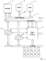
- FIG. 1 is a general high level block diagram of a computer system.
- the system of the present invention will initially be considered at this level, and at a number of successive, more detailed levels, to ensure a full understanding and appreciation of the role and operation of the present invention in an environment in which it could be usefully employed.
- FIG. 1 shows a personal computer system employing the system of the present invention and illustrates four main buses which represent the major interfaces between the various components at the top level.
- a first memory connector 2 and a second memory connector 4 comprise private interfaces between processors 6, 8 and their respective dedicated memories 10, 12 and 14.
- a processor bus 16 is the multiple master bus which is the architectural break between the processing units, which include processors 6 and 8, and an I/0 channel 20 comprising a standard interface which may be either ISA, EISA or microchannel.
- the processor bus 16 performs various functions. First, it serves as an interconnection among the processors 6, and 8, and the intelligent I/0, and/or processor 14; all system memory 10, 12 and optional memory 14; and the system I/0 channel 20 and its I/0 expansion slots 22 - 40.
- System memory 10, 12 and 14 may be configured as a virtual 64 bit interleaved memory with two associated banks for storage of one 32 bit double word each, one odd and one even.
- the processor bus 16 allows each processor 6, 8 to access another processor's 8, 6 memory. This access is allowed "through" the processor that is directly connected to the memory.
- processor bus 16 serves as a communication link between processors 6, 8 and 14.
- the processor bus 16 also acts as the interface between the processor memory complexes 10, 12, and 14 and the I/0 channel 20. Addresses and data are transferred under control of a system and bus controller 42 between the processor bus 16 and the I/0 channel 20 through a set of transceivers 44 and 46 which may comprise Model 74ALS245 transceivers made by Texas Instruments Incorporated. Through this interface, a processor bus master can access the system I/0 and peripherals 18 as well as each of the I/0 expansion slots 22, 24, 26, 28, 30, 32, 34, 36, 38, 40. Still further, the processor bus 16 also acts as the data communications path for I/0 to I/0 accesses. The system and bus controller 42 generates "action codes" which format the protocols necessary for inter-device communication and thereby enable intelligent cards of wide diversity to be plugged into an I/0 expansion slot and access other I/0 cards or even the processors and memory connected to the processor bus 16.
- action codes which format the protocols necessary for inter-device communication and thereby enable intelligent cards of wide diversity to be plugged
- the system and bus controller 42 in addition to providing routing information and action code generation, handles all processor bus 16 arbitration and interfaces all control signals to the system I/0 bus 20, such as ISA "commands", DMA control signals, and interrupts.
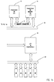
- FIG. 2 there is shown a block diagram of the major components of a processor card employed in the computer system of FIG. 1.
- the processor module 6 can be seen to interface with the rest of the computer system through the memory connector 2 and the processor bus 16.
- Processor module 6 includes a microprocessor 48 (e.g., an Intel 80386), a numeric coprocessor 50 (e.g., an Intel 80387), an optional coprocessor 52 (e.g., a Weitek 3167), a cache subsystem, a clock circuit 54, a POST ROM (Power On, Self Test, Read Only Memory) 56, a data flow and ECC controller 58, and a memory and bus controller 60.
- a microprocessor 48 e.g., an Intel 80386
- a numeric coprocessor 50 e.g., an Intel 80387
- an optional coprocessor 52 e.g., a Weitek 3167
- a cache subsystem e.g., a clock circuit 54
- POST ROM Power On, Self Test, Read Only Memory
- ECC controller 58 e.g., a data flow and ECC controller
- the cache subsystem includes a cache memory (shown as consisting of two separate banks 62A, 62B of SRAMs and a cache controller 64 (e.g., an Intel 82385).
- the cache subsystem functions as an extremely fast, "sketchpad-like" memory which provides rapid access to the data most frequently needed by the processor.
- the system may employ cache memory with cache line sizes of 4 double words each so that if a cacheable read is made by the processor, the memory controller returns 4 sequential double words into the cache from system memory. Optimizing the accuracy with which this operation occurs from a pair of interleaved 32 bit, double word memory banks and through error correction and/or detection circuitry is one of the principal goals of the system of the present invention as discussed below.
- a snoop address latch 66 would likely be included to capture each processor address that is generated in order to invalidate addresses if necessary.
- a programmable array logic (PAL) line extension logic 68 would likely also be included to control address and control signals passing between the cache 62A, 62B, cache controller 64, and memory and bus controller 60.
- the processor module 6 also includes local address, data and control buses (indicated by the various arrows shown in FIG. 2) that interconnect the microprocessor 48, coprocessors 50, 52 and cache 62A, 62B, as well as the data flow and ECC controller 58 and memory and bus controller 60. These buses are used for local cycles such as ROM 56 reads, coprocessor cycles and cache read hits. Access to the ROM 56 can be accomplished via operation of the data flow and ECC controller 58 and memory and bus controller 60. For global cycles such as cache writes, cache read misses, non-cacheable cycles, and I/0 cycles, however, the processor module 6 must complete its access off-board.
- the memory and bus controller 60 decodes the local address and control signals and determines whether the access is destined for the processor bus 16 or for the dedicated memory. For a memory cycle, the memory and bus controller 60 generates the memory control signals (i.e., RAS, CAS and WE) and addresses to access the memory card. The memory and bus controller 60 also generates refresh signals to the memory card, e.g., element 10, for each refresh period. In conjunction with the memory bus controller 60, the data flow and ECC controller 58 also performs error checking and correction.
- the memory control signals i.e., RAS, CAS and WE
- the memory and bus controller 60 also generates refresh signals to the memory card, e.g., element 10, for each refresh period.
- the data flow and ECC controller 58 also performs error checking and correction.
- the memory and bus controller 60 For off-board cycles that are not destined for the memory card 10, the memory and bus controller 60 generates a processor bus request signal and takes control of the processor bus 16 when it is granted. Again, working in conjunction with the data flow and ECC controller 58, the memory and bus controller 60 completes the access to the processor bus 16.
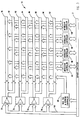
- FIG. 3 a block diagram of the major components of a memory card 10 is set forth therein.
- the memory card 10 interfaces to the rest of the system through the memory connector 2.
- each memory card 10 preferably implements storage of virtual 64 bit words in the form of 2 interleaved banks of 32 bit double words, one odd and one even.
- Each card 10 includes a RAS, CAS, and refresh controller 68, four address buffers 70, 72, 74, 76, eight single in-line memory (SIMM) slots 78, 80, 82, 84, 86, 88, 90, 92, and four interleave controllers 94, 96, 98, 100.
- the RAS, CAS, and refresh controller 68 receives control signals from the memory interface 102 (See FIG. 1), which is driven by the memory and bus controller 60 (see FIG.
- Each of the four interleave controllers 94, 96, 98, 100 multiplexes eight bits of data between the memory connector 2 and the SIMM slots 78, 80, 82, 84, 86, 88, 90, 92.
- each memory card 10 and 12 includes address buffers 70, 72, 74, 76 and SIMM slots 78, 80, 82, 84, 86, 88, 90, 92.
- Model 74FCT828 and 74FCT827 data buffers manufactured by VTC could be used as the address buffers 70, 72, 74, 76.
- Inverting (74FCT828's) and non-inverting (74FCT827's) buffers are used to minimise the average address line signal switching to minimise electrical noise.
- the SIMM slots 78, 80, 82, 84, 86, 88, 90, 92 can be adapted to accommodate either 1, 2, 4 or 8 Mbyte SIMMs with either parity or ECC organization.
- the address buffers 70, 72, 74, 76 and the SIMM slots 78, 80, 82, 84, 86, 88, 90, 92 play important roles in the system and method of a preferred embodiment of the present invention and are thus discussed in detail below.
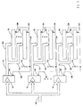
- FIG. 4 a block diagram of a prior art memory circuit is shown therein.
- this circuit corresponds to what could be a portion of FIG. 3. More specifically, that portion could include, for example, address buffers 70, 72, 74 and corresponding SIMM sockets 78, 80, 82, 84, 86, 88. While pairs of SIMM sockets are shown associated with each single buffer, e.g., sockets 78, 80 with buffer 70, only one or three or more SIMM sockets could be associated with each buffer.
- address data travels through line 102, from memory connector 2 as can be seen in FIG. 3, and is collected in the various address buffers 70, 72, 74.
- inverting or non inverting buffers 74FCT828's and 74FCT827's, repectively, both manufactured by VTC could be employed for such buffers.
- address buffers of this type have an output enable pin 104, 106, 108. When an output enable pin, e.g., pin 104 of buffer 70, is low, the buffer is in an enabled state. When, on the other hand, the output enable pin 104 is high, the associated buffer 70 is disabled.
- the address data After being buffered in the address buffer 70, the address data passes through, lines 110, 112 and 114 respectively, to SIMM sockets 78, 80 into which SIMMs could be installed. Signals from the address buffers 70 - 74 drive the address lines of the DRAM memory chips mounted in the SIMMs plugged into the sockets 78 - 88 in order to access the memory.
- FIG. 4 may be considered to have three SIMMs installed in the six available SIMM sockets, for example, in slots 78, 80 and 82.
- FIG. 5 there is shown a circuit similar to the one shown in FIG. 4, although it has been modified according to the teachings of the present invention.
- the memory circuit of FIG 5 includes line 102; address buffers 70, 72, 74 with output enable pins 104, 106, 108; SIMM sockets or slots 78, 80, 82, 84, 86, 88; and address data lines 110, 112, 114, 116, 118, 120, 122, 124, 126, interconnecting certain of the buffers 70, 72, 74 and certain of the SIMM sockets 78, 80, 82, 84, 86, 88.
- Each of these elements of the memory circuit are commnon to both the prior art configuration shown in FIG. 4 and the configuration constructed according to the system embodying the present invention shown in FIG. 5.
- SIMM 128 comprises a plurality of DRAMs 130, 132... 134 mounted on a small rectangular printed circuit board 136, with a plurality of pins; e.g., pins 138, 140, 142, including a PRES pin 146.
- PRES pin 146 of SIMM 128 is grounded on the printed circuit board of SIMM 128.
- modified SIMMs 128, as shown and discussed above in connection with FIG. 6, can be installed in each of the various SIMM sockets 78, 80, 82, 84, 86, 88.
- modified SIMMs 128 are installed only in sockets 78, 80 and 82 and sockets 84, 86, and 88 remain empty.
- FIG. 5 differs from FIG. 4 in that, rather than being grounded, the output enable pins 104, 106, 108 of the various address buffers 70, 72, 74 are connected to points 150, 152, 154, 156, 158, 160 on the SIMM sockets 78, 80, 82, 84, 86, 88. According to the teachings of the present embodiment these points 150, 152, 154, 156, 158, 160 are positioned to contact the grounded PRES pins (e.g., pin 146) of SIMMs 128 installed in the various sockets 78, 80, 82, 84, 86, 88.
- the grounded PRES pins e.g., pin 146
- the lines 162, 164, 166 interconnecting pins 104, 106, 108 and points 150, 152, 154, 156, 158, 160 have pull-up resistor portions 170, 172, 174 connected thereto.
- an embodiment of the present invention provides a relatively simple and inexpensive system and method for properly driving address data to memory modules if those modules are present, but the driving of empty sockets with unterminated address signals is substantially reduced. This reduction in needless driving signals reduces current draw and circuit noise and improves overall system performance.
- each SIMM socket could have its own address buffer. If such a system included the lines and pull-up resistors of embodiments the present invention even more unnecessary current draw and noise could be eliminated.
- an embodiment of the present invention will improve system performance in every case in which all of a number of sockets associated with a particular address buffer are empty. Many other modifications and variations are possible.
Landscapes
- Engineering & Computer Science (AREA)
- Theoretical Computer Science (AREA)
- Physics & Mathematics (AREA)
- General Engineering & Computer Science (AREA)
- General Physics & Mathematics (AREA)
- Dram (AREA)
- Techniques For Improving Reliability Of Storages (AREA)
- Memory System (AREA)
Description
- The present invention relates to memory systems and, more particularly, to memory systems including memory modules and associated address buffers.
- Digital data processing systems generally comprise a central processing unit (CPU), a main memory and one or more input/output devices such as card readers, magnetic tape readers, magnetic disks and printers, which are interfaced to the CPU and main memory via input/output controllers (IOC). In typical data processing systems, the amount of main memory in the system can usually be varied from some minimal amount to some maximum amount with the user of the data processing system determining the amount of memory to be actually installed within each particular system. Additional quantities of main memory, usually packaged in incremental units can be added to a system as they are needed. The amount of main memory installed into a computer system is usually a function of the size and number of computer programs to be executed, the amount of data to be processed, and the speed with which the data must be processed. Therefore, in a typical data processing system, the amount of main memory actually configured within a particular system is less than the maximum amount of memory which could be configured.
- Typically, the main memory within a computer is composed of dynamic random-access memory (DRAM) chips. As their name suggests, DRAM chips offer the possibility of calling any data word stored in memory to the CPU independently of its multitudinous neighbors. This is assured because DRAM chips store individual bits of data in multiple rows and columns of cells which provide each data bit with its own unique address. Address buffers are used to receive signals from a memory controller which are indicative of the particular rows and columns of cells within the DRAM chips which are to be accessed by the CPU. The address buffers actually apply to the memory chips the signals which are necessary in order to store and retrieve data in the cells of the chips. Around 1983, Wang Laboratories announced development of a method of packaging DRAMs that significantly reduced cost and space requirements of computer memory. The product of development was a single in line memory module or SIMM that integrated nine separate 64K RAM chips into a .75 x 3-inch space. SIMMs, which are essentially small pc boards with arrays of memory chips contained in plastic leaded chip carriers surface mounted on one or both sides of the boards, have evolved so that they now typically hold either nine 1M-bit DRAMs or nine 256K-bit DRAMs. SIMMs are generally installed in connector sokets to make them easily added to a system and avoid the difficulty and risks of soldering the SIMMs directly to a pc board.
- As an underlying reason for certain problems solved by the system and method of the present invention, it should be appreciated that in the computer arts efforts are made to keep the number of components to a minimum, but to use each component to the fullest extent possible in order to optimize the compactness and efficiency of each system. In computer memory packaging, each DRAM SIMM could have its own individually associated address buffer, however, a single address buffer has often been employed to drive two DRAM SIMMs. As computer systems frequently include more than one pair of DRAM SIMMs, it is common to have a multitude of pairs of DRAM SIMMs mounted in sockets with each pair of SIMMs having a single address buffer associated with it.
- As discussed above, computer memories are generally configured with less than the minimum amount of memory possible being actually installed in the system. Such systems are most efficiently made by initially equipping them with a full complement of address buffers and SIMM sockets for mounting memory components but only installing the number of memory components which are initially needed in the system, as selected by the user. Thus, it is likely that less than all of the SIMM sockets of a new system will have memory components actually installed in them. Adding memory later as it is needed can be quickly and easily accomplished toy simply putting a memory component, e.g., a SIMM, into an empty socket since the address buffer is already present in the system to access that newly added memory.
- Notwithstanding the clear efficiencies and desirable attributes of designs such as those mentioned above, such designs have had a number of deficiencies and shortcomings. For example, in order to ensure that the address buffers are capable of immediately driving a memory module newly installed in a socket, those address buffers must be kept in a constantly enabled state. While constantly enabling the address buffers for all SIMM sockets guarantees their ability to drive address lines (i.e., column and row information going to DRAMs) to, e.g., a DRAM SIMM if and when it is installed, if a SIMM is not installed, the address buffer still drives address lines. Unnecessary voltage output signals from address buffers are a source of both excess current draw and electrical noise within the system. Excess current draw is undesirable because system power consumption is increased and noise, in the form of electromagnetic interference (EMI) caused by rapid switching of address buffer signals, is undesirable because it can produce data errors.
- Other systems have addressed these problems by providing for the enablement of address buffers by means of manually operated DIP switches or jumpers used to configure system memory. However, reliance upon a user to manually, and correctly, activate switches or install jumpers is not a reliable solution in a complex computer memory system.
- Based on the foregoing it should be appreciated that there are good reasons for keeping an address buffer associated with a memory module constantly enabled, however, shortcoming and deficiencies are associated with such a design. The preferred prior art solutions to the these problems have proven to be inadequate.
- An embodiment of the present invention overcomes the shortcomings and deficiencies of the prior art by providing a memory circuit including interconnection means for a plurality of memory
- United States Patent No. 4787060 discloses a method of determining the maximum amount of physical memory present in a data processing system that can be configured to have one or more memory modules where the memory modules may be one of several types having different amounts of memory locations. Signals indicate the presence of a memory module and the module type while a diagnostic process determines the amount of memory present in the system.
- The present invention provides an internal main memory system for a computer, the system being of variable capacity, including a plurality of connection means to which respective memory units are connectable, the capacity of the memory system being determined by the number of memory units connected to connection means and sensing means for sensing that a connection means has a memory unit connected to it, wherein, in order to reduce the electrical noise within the computer, the memory system includes a plurality of drive means connected to respective connection means for supplying selected drive signals to the respective connection means and signalling means so connecting the sensing means to the plurality of drive means that drive signals are provided by the drive means only to the respective connection means for which the signalling means signals the connection of memory units.
- Preferably, the sensing means includes a sensing terminal on each connection means and the sensing terminal on each connection means is connected to the signalling means.
- Preferably, the plurality of drive means include a plurality of drive buffers including control terminals, the control terminals being connected by signalling lines to the sensing terminals.
- Preferably, the control terminals of the drive buffers are connected to a reference voltage by way of a resistor and the sensing terminals of the connection means are connected to the control terminals and, preferably, the selected drive signals are address signals.
- The present invention provides a method of operating an internal main memory system in a computer, the memory system being of variable capacity determined by the number of memory units installed, includes the step of sensing which of a plurality of connection means have memory units connected to them, wherein, in order to reduce the electrical noise within the computer, the presence or absence of a memory unit at each of the plurality of connection means is signalled to respective drive means and selected drive signals are supplied by the respective drive means only to those connection means for which the presence of memory units is signalled.
- Preferably, the step of supplying selected drive signals only to those connection means for which the presence of memory units is signalled is the step of supplying address signals only to those connection means for which the presence of memory units is signalled. modules, which memory module may or may not be present, and means for transmitting address signal to the memory modules if, and only if, the memory modules are present.
- Certain embodiments of the present invention may also include at least one address buffer connected in circuit between a central processing unit and the memory module interconnection means and the interconnection means may include sockets into which the memory modules may be installed. In other aspects of embodiments of the present invention, the means for transmitting address signals to the memory modules if, and only if, the memory modules are present includes means for disabling the at least one address buffer if memory modules are not installed in the sockets.
- In other embodiments of the present invention, there may be at least two sockets for DRAM SIMMs, the at least two sockets being driven by a single address buffer. In such an embodiment, a line having a pull-up resistor portion interconnects an output enable pin on the single address buffer and grounded PRES pins on each DRAM SIMM installed in the at least two sockets. Further, in such an embodiment, absence of both DRAM SIMMs would, because of the pull-up resistor, disable the address buffer by driving the output enable line high. On the other hand, presence of one or both of the DRAM SIMMs would drive the output enable line low, enabling the address buffer.
- A method embodying the teachings of the present invention includes the steps of passing address signals to connectors for receiving memory modules using disableable address buffering means, and disabling the disableable buffering means if memory modules, to which the address signals are being sent, are not present.
- A computer system incorperating the invention can comprise:
- a processor;
- a memory operatively connected to said processor; and
- a memory controller operatively connected to said memory wherein said memory comprises:
- interconnection means for a plurality of memory modules, which memory modules may or may not be present, and
- means for transmitting address signals to said interconnection means if and only if memory modules are present within said interconnection means.
-
- The said memory of the computer system can comprise at least one address buffer connected to transmit address signals to said interconnection means.
- The said interconnection means can comprise sockets into which said memory modules may be installed.
- The said means for transmitting said address signals to said interconnection means if and only if memory modules are present can comprise means for disabling said at least one address buffer from transmitting address signals if memory modules are not installed in said sockets.
- The said interconnection means can comprise at least two sockets into which separate memory modules can be installed and wherein said at least two sockets are driven by a single address buffer.
- The said at least two sockets can be capable of receiving and interconnecting single in line memory modules (SIMMs) into said memory circuit.
- The said at least two sockets can interconnect at least two SIMMs and said SIMMs each include a plurality of DRAM chips forming the memory cells thereby.
- The said DRAM SIMMs installed in said at least two sockets can have grounded PRES pins.
- The said single address buffer can include an output enable pin.
- The said means for transmitting said address signals to said interconnection means if and only if said memory modules are present can include means for disabling said single address buffer if no DRAM SIMMs are installed in said interconnection means, said means for disabling said single address buffer if no DRAM SIMMs are installed comprising conductors interconnecting said output enable pin of said single address buffer to the grounded PRES pins of DRAM SIMMs that may be installed in either or both of said at least two sockets.
- The said lines interconnecting said output enable pin of said single address buffer to grounded PRES pins of DRAM SIMMs which can be installed in said at least two sockets can include a pull-up resistor.
- The said memory can further comprise a RAS, CAS and refresh controller means operatively connected to said interconnection means.
- An embodiment of the present invention provides a method of addressing interconnecting means for memory modules, which interconnection means may or may not have memory modules connected thereto, comprising the steps of:
- buffering address signals sent to said interconnection means in at least one address buffer; and
- disabling said at least one address buffer if said interconnection means has no memory modules connected thereto.
-
- Preferably, the said step of disabling said at least one address buffer if said interconnection means has no memory modules connected thereto comprises the step of driving the output enable of said address buffer high if said interconnection means has no memory module connected thereto.
- Accordingly, it is an object of the present invention to disable drive means associated with optional memory modules, when those optional memos modules are not present.
- Another object of the present invention is to avoid the driving of lines with no loads being present on those lines, which driving causes the drawing of excess current and the generation of excess electrical noise, both of which are undesirable circuit characteristics in a computer memory system.
- For a more complete understanding of the present invention, and for further objects and advantages thereof, reference may now be had to the following description taken in conjunction with the accompanying drawings in which:
- FIG. 1 is a block diagram of a computer system which employs the memory configuration of the present invention;
- FIG. 2 is a block diagram of a processor module used in the computer system of FIG. 1.
- FIG. 3 is a block diagram of a memory module employed in the computer system of FIG. 1; and
- FIG. 4 is a block diagram of a prior art memory circuit;
- FIG. 5 is a block diagram of a memory circuit according to the teachings of the present invention; and
- FIG. 6 is a schematic view of a DRAM SIMM modifed for use in a memory circuit according to the present invention.
-
- Referring now to the drawings wherein like reference numerals designate identical or similar elements throughout the several views, depicted in FIG. 1 is a general high level block diagram of a computer system. The system of the present invention will initially be considered at this level, and at a number of successive, more detailed levels, to ensure a full understanding and appreciation of the role and operation of the present invention in an environment in which it could be usefully employed.
- FIG. 1 shows a personal computer system employing the system of the present invention and illustrates four main buses which represent the major interfaces between the various components at the top level. A
first memory connector 2 and asecond memory connector 4 comprise private interfaces betweenprocessors dedicated memories processor bus 16 is the multiple master bus which is the architectural break between the processing units, which includeprocessors channel 20 comprising a standard interface which may be either ISA, EISA or microchannel. - The
processor bus 16 performs various functions. First, it serves as an interconnection among theprocessors processor 14; allsystem memory optional memory 14; and the system I/0channel 20 and its I/0 expansion slots 22 - 40.System memory processor bus 16 allows eachprocessor processor bus 16 requests access to a location in some other processor's memory, the other processor completes the access locally, receiving the address from theprocessor bus 16 and transferring the data from and to theprocessor bus 16. Additionally, theprocessor bus 16 serves as a communication link betweenprocessors - In addition to the foregoing, the
processor bus 16 also acts as the interface between theprocessor memory complexes channel 20. Addresses and data are transferred under control of a system andbus controller 42 between theprocessor bus 16 and the I/0channel 20 through a set oftransceivers 44 and 46 which may comprise Model 74ALS245 transceivers made by Texas Instruments Incorporated. Through this interface, a processor bus master can access the system I/0 andperipherals 18 as well as each of the I/0expansion slots processor bus 16 also acts as the data communications path for I/0 to I/0 accesses. The system andbus controller 42 generates "action codes" which format the protocols necessary for inter-device communication and thereby enable intelligent cards of wide diversity to be plugged into an I/0 expansion slot and access other I/0 cards or even the processors and memory connected to theprocessor bus 16. - The system and
bus controller 42, in addition to providing routing information and action code generation, handles allprocessor bus 16 arbitration and interfaces all control signals to the system I/0bus 20, such as ISA "commands", DMA control signals, and interrupts. - Referring now to FIG. 2, there is shown a block diagram of the major components of a processor card employed in the computer system of FIG. 1. With reference to FIG. 1, the
processor module 6 can be seen to interface with the rest of the computer system through thememory connector 2 and theprocessor bus 16. -
Processor module 6 includes a microprocessor 48 (e.g., an Intel 80386), a numeric coprocessor 50 (e.g., an Intel 80387), an optional coprocessor 52 (e.g., a Weitek 3167), a cache subsystem, a clock circuit 54, a POST ROM (Power On, Self Test, Read Only Memory) 56, a data flow andECC controller 58, and a memory andbus controller 60. - The cache subsystem includes a cache memory (shown as consisting of two
separate banks - For systems with a
cache address latch 66 would likely be included to capture each processor address that is generated in order to invalidate addresses if necessary. Additionally, in systems with a cache memory, a programmable array logic (PAL)line extension logic 68 would likely also be included to control address and control signals passing between thecache cache controller 64, and memory andbus controller 60. - The
processor module 6 also includes local address, data and control buses (indicated by the various arrows shown in FIG. 2) that interconnect themicroprocessor 48,coprocessors cache ECC controller 58 and memory andbus controller 60. These buses are used for local cycles such asROM 56 reads, coprocessor cycles and cache read hits. Access to theROM 56 can be accomplished via operation of the data flow andECC controller 58 and memory andbus controller 60. For global cycles such as cache writes, cache read misses, non-cacheable cycles, and I/0 cycles, however, theprocessor module 6 must complete its access off-board. - For off-board cycles, the memory and
bus controller 60 decodes the local address and control signals and determines whether the access is destined for theprocessor bus 16 or for the dedicated memory. For a memory cycle, the memory andbus controller 60 generates the memory control signals (i.e., RAS, CAS and WE) and addresses to access the memory card. The memory andbus controller 60 also generates refresh signals to the memory card, e.g.,element 10, for each refresh period. In conjunction with thememory bus controller 60, the data flow andECC controller 58 also performs error checking and correction. - For off-board cycles that are not destined for the
memory card 10, the memory andbus controller 60 generates a processor bus request signal and takes control of theprocessor bus 16 when it is granted. Again, working in conjunction with the data flow andECC controller 58, the memory andbus controller 60 completes the access to theprocessor bus 16. - Referring now to FIG. 3, a block diagram of the major components of a
memory card 10 is set forth therein. With reference to FIG. 1, thememory card 10 interfaces to the rest of the system through thememory connector 2. - As discussed above, each
memory card 10 preferably implements storage of virtual 64 bit words in the form of 2 interleaved banks of 32 bit double words, one odd and one even. Eachcard 10 includes a RAS, CAS, and refreshcontroller 68, fouraddress buffers slots interleave controllers controller 68 receives control signals from the memory interface 102 (See FIG. 1), which is driven by the memory and bus controller 60 (see FIG. 2), and then, in turn, drives the control signals to theSIMM slots interleave controllers memory connector 2 and theSIMM slots - As previously mentioned, each
memory card SIMM slots SIMM slots SIMM slots - Referring now to FIG. 4, a block diagram of a prior art memory circuit is shown therein. In general, this circuit corresponds to what could be a portion of FIG. 3. More specifically, that portion could include, for example, address buffers 70, 72, 74 and
corresponding SIMM sockets sockets buffer 70, only one or three or more SIMM sockets could be associated with each buffer. - In the prior art configuration of FIG. 4, it should be appreciated that address data travels through
line 102, frommemory connector 2 as can be seen in FIG. 3, and is collected in the various address buffers 70, 72, 74. As previously mentioned, either inverting or non inverting buffers 74FCT828's and 74FCT827's, repectively, both manufactured by VTC, could be employed for such buffers. As is well known to those skilled in the art, address buffers of this type have an output enablepin buffer 70, is low, the buffer is in an enabled state. When, on the other hand, the output enablepin 104 is high, the associatedbuffer 70 is disabled. - After being buffered in the
address buffer 70, the address data passes through,lines SIMM sockets - As mentioned above in the description of related art section, it is not uncommon in commercially shipped computer systems for a number of SIMM memory sockets not to have SIMMs installed therein. This is because computer systems are frequently sold with less than the maximum possible memory being actually installed. Such systems provide for quick and easy memory expansion and upgrading in the form of empty slots, ready to accept a memory module. For purposes of illustration of the system of the present invention, the configuration of FIG. 4 may be considered to have three SIMMs installed in the six available SIMM sockets, for example, in
slots - It can be seen in FIG. 4 illustrating the prior art, the output enable
pins buffers various buffers SIMM slots slot pair slot pair empty slots - Referring now to FIG. 5 there is shown a circuit similar to the one shown in FIG. 4, although it has been modified according to the teachings of the present invention. The memory circuit of FIG 5 includes
line 102; address buffers 70, 72, 74 with output enablepins slots address data lines buffers SIMM sockets - Referring briefly to FIG. 6, there is shown, in partial schematic form, a
SIMM 128.SIMM 128 comprises a plurality ofDRAMs circuit board 136, with a plurality of pins; e.g., pins 138, 140, 142, including aPRES pin 146. According to one aspect of the teaching of the present embodiment, PRES pin 146 ofSIMM 128 is grounded on the printed circuit board ofSIMM 128. - Referring again to FIG. 5, modified
SIMMs 128, as shown and discussed above in connection with FIG. 6, can be installed in each of thevarious SIMM sockets SIMMs 128 are installed only insockets sockets - Comparing FIG. 5 to FIG. 4, it may be seen that the configuration of FIG. 5 differs from FIG. 4 in that, rather than being grounded, the output enable
pins points SIMM sockets points SIMMs 128 installed in thevarious sockets lines pins resistor portions - With the configuration shown in FIG. 5, if
SIMMs 128 are installed in both sockets of a pair ofSIMM sockets pin 104 would be driven low and the associatedaddress buffer 70 will be enabled, in which case address signals will be forwarded throughbuffer 70 toSIMMs 128 installed insockets socket 86 nor 88,line 166 and pull-upresistor 174 will operate to drive the output enable ofaddress buffer 74 high, which will disable it from producing output signals. Thus,address buffer 74 will not needlessly attempt to drive absent SIMMs with address signals which go nowhere. Finally, if a SIMM is installed in only one socket of a pair, e.g., only insocket 82 ofsocket pair address buffer 72 will be enabled and the installedSIMM 128 will be properly driven. - Based upon the foregoing, it should be appreciated that an embodiment of the present invention provides a relatively simple and inexpensive system and method for properly driving address data to memory modules if those modules are present, but the driving of empty sockets with unterminated address signals is substantially reduced. This reduction in needless driving signals reduces current draw and circuit noise and improves overall system performance.
- Obviously, numerous modifications and variations are possible in view of the above teachings. For example, each SIMM socket could have its own address buffer. If such a system included the lines and pull-up resistors of embodiments the present invention even more unnecessary current draw and noise could be eliminated. Of course, there is a cost/efficiency tradeoff in selecting the number of address buffers and SIMM sockets to be employed in a system. In any event, an embodiment of the present invention will improve system performance in every case in which all of a number of sockets associated with a particular address buffer are empty. Many other modifications and variations are possible.
Claims (8)
- An internal main memory system for a computer, the system being of variable capacity, including a plurality of connection means (78, 80, 82, 84, 86, 88) to which respective memory units (128) are connectable, the capacity of the memory system being determined by the number of memory units connected to connection means (78, 80, 82, 84, 86, 88) and sensing means (150, 152, 154, 156, 158, 160) for sensing that a connection means (78, 80, 82, 84, 86, 88) has a memory unit (128) connected to it, characterised in that, in order to reduce the electrical noise within the computer, the memory system includes a plurality of drive means (70, 72, 74) connected to respective connection means (78, 80, 82, 84, 86, 88) for supplying selected drive signals to the respective connection means (78, 80, 82, 84, 86, 88) and signalling means (104, 162, 170; 106, 164, 172; 108, 166, 174) so connecting the sensing means (150, 152, 154, 156, 158, 160) to the plurality of drive means (70, 72, 74) that drive signals are provided by the drive means (70, 72, 74) only to the respective connection means (78, 80, 82, 84, 86, 88) for which the signalling means (104, 162, 170; 106, 164, 172; 108, 166, 174) signals the connection of memory units (128).
- A memory system as claimed in claim 1, wherein the sensing means (150, 152, 154, 156, 158, 160) includes a sensing terminal (150, 152, 154, 156, 158, 160) on each connection means (78, 80, 82, 84, 86, 88) and the sensing terminal (150, 152, 154, 156, 158, 160) on each connection means (78, 80, 82, 84, 86, 88) is connected to the signalling means (104, 162, 170; 106, 164, 172; 108, 166, 174).
- A memory system as claimed in claim 2, wherein the plurality of drive means (70, 72, 74) include a plurality of drive buffers (70, 72, 74) including control terminals (104, 106, 108), the control terminals (104, 106, 108) being connected by signalling lines (162, 164, 166) to the sensing terminals (150, 152, 154, 156, 158, 160).
- A memory system as claimed in claim 3, wherein the control terminals (104, 106, 108) of the drive buffers (70, 72, 74) are connected to a reference voltage by way of a resistor (170, 172, 174) and the sensing terminals (150, 152, 154, 156, 158, 160) of the connection means (78, 80, 82, 84, 86, 88) are connected to the control terminals (104, 106, 108).
- A memory system as claimed in any one of claims 1 to 4, wherein the selected drive signals are address signals.
- A computer system including a memory system as claimed in any one of claims 1 to 5.
- A method of operating an internal main memory system in a computer, the memory system being of variable capacity determined by the number of memory units (128) installed, including the step of sensing which of a plurality of connection means (78, 80, 82, 84, 86, 88) have memory units (128) connected to them, characterised in that, in order to reduce the electrical noise within the computer, the presence or absence of a memory unit at each of the plurality of connection means is signalled to respective drive means (70, 72, 74) and selected drive signals are supplied by the respective drive means (70, 72, 74) only to those connection means (78, 80, 82, 84, 86, 88) for which the presence of memory units (128) is signalled.
- A method of operating a memory system as claimed in claim 7, wherein the step of supplying selected drive signals only to those connection means (78, 80, 82, 84, 86, 88) for which the presence of memory units (128) is signalled is the step of supplying address signals only to those connection means (78, 80, 82, 84, 86, 88) for which the presence of memory units (128) is signalled.
Applications Claiming Priority (2)
| Application Number | Priority Date | Filing Date | Title |
|---|---|---|---|
| US540651 | 1990-06-19 | ||
| US07/540,651 US5241643A (en) | 1990-06-19 | 1990-06-19 | Memory system and associated method for disabling address buffers connected to unused simm slots |
Publications (3)
| Publication Number | Publication Date |
|---|---|
| EP0462786A2 EP0462786A2 (en) | 1991-12-27 |
| EP0462786A3 EP0462786A3 (en) | 1992-01-29 |
| EP0462786B1 true EP0462786B1 (en) | 2000-02-02 |
Family
ID=24156371
Family Applications (1)
| Application Number | Title | Priority Date | Filing Date |
|---|---|---|---|
| EP91305482A Expired - Lifetime EP0462786B1 (en) | 1990-06-19 | 1991-06-18 | Address-enabling system and method for memory modules |
Country Status (4)
| Country | Link |
|---|---|
| US (1) | US5241643A (en) |
| EP (1) | EP0462786B1 (en) |
| JP (2) | JPH04233046A (en) |
| DE (1) | DE69131948T2 (en) |
Families Citing this family (32)
| Publication number | Priority date | Publication date | Assignee | Title |
|---|---|---|---|---|
| US5430681A (en) * | 1989-05-08 | 1995-07-04 | Hitachi Maxell, Ltd. | Memory cartridge and its memory control method |
| JPH0715665B2 (en) * | 1991-06-10 | 1995-02-22 | インターナショナル・ビジネス・マシーンズ・コーポレイション | Personal computer |
| US5428762A (en) * | 1992-03-11 | 1995-06-27 | International Business Machines Corporation | Expandable memory having plural memory cards for distributively storing system data |
| US5379304A (en) * | 1994-01-28 | 1995-01-03 | International Business Machines Corporation | Method and structure for providing error correction code and parity for each byte on SIMM's |
| US5623506A (en) * | 1994-01-28 | 1997-04-22 | International Business Machines Corporation | Method and structure for providing error correction code within a system having SIMMs |
| US5465262A (en) * | 1994-01-28 | 1995-11-07 | International Business Machines Corporation | Method and structure for providing error correction code and automatic parity sensing |
| US5541941A (en) * | 1994-01-28 | 1996-07-30 | International Business Machines Corporation | Method and structure for providing automatic parity sensing |
| US5450422A (en) * | 1994-01-28 | 1995-09-12 | International Business Machines Corporation | Method and structure for providing error correction code for each byte on SIMM'S |
| DE4423567C2 (en) * | 1994-07-05 | 1998-09-03 | Siemens Ag | Module card |
| EP0735478A1 (en) * | 1995-03-31 | 1996-10-02 | BULL HN INFORMATION SYSTEMS ITALIA S.p.A. | Variable configuration data processing system with automatic serial test interface connection configuration and bypass device |
| US5621678A (en) * | 1995-04-13 | 1997-04-15 | Digital Equipment Corporation | Programmable memory controller for power and noise reduction |
| US5737572A (en) * | 1995-06-06 | 1998-04-07 | Apple Computer, Inc. | Bank selection logic for memory controllers |
| US5940586A (en) * | 1995-10-16 | 1999-08-17 | International Business Machines Corporation | Method and apparatus for detecting the presence of and disabling defective bus expansion devices or Industry Standard Architecture (ISA) adapters |
| EP0782076A1 (en) * | 1995-12-29 | 1997-07-02 | Siemens Aktiengesellschaft | Arrangement for detecting the configuration of a memory |
| US5745914A (en) * | 1996-02-09 | 1998-04-28 | International Business Machines Corporation | Technique for converting system signals from one address configuration to a different address configuration |
| US5802395A (en) * | 1996-07-08 | 1998-09-01 | International Business Machines Corporation | High density memory modules with improved data bus performance |
| US5786769A (en) * | 1996-12-11 | 1998-07-28 | International Business Machines Corporation | Method and system for detecting the presence of adapter cards |
| TW379466B (en) * | 1997-12-27 | 2000-01-11 | Via Tech Inc | Memory module slot device providing constant loads |
| JP3765192B2 (en) | 1998-10-28 | 2006-04-12 | 株式会社日立製作所 | Directional coupled bus system |
| US6286066B1 (en) | 1998-12-15 | 2001-09-04 | Dell U.S.A., L.P. | Hot-plug interface for detecting adapter card insertion and removal |
| US6357018B1 (en) | 1999-01-26 | 2002-03-12 | Dell Usa, L.P. | Method and apparatus for determining continuity and integrity of a RAMBUS channel in a computer system |
| JP3880286B2 (en) | 1999-05-12 | 2007-02-14 | エルピーダメモリ株式会社 | Directional coupled memory system |
| JP3820843B2 (en) * | 1999-05-12 | 2006-09-13 | 株式会社日立製作所 | Directional coupled memory module |
| US6408356B1 (en) | 1999-11-16 | 2002-06-18 | International Business Machines Corporation | Apparatus and method for modifying signals from a CPU to a memory card |
| US6647434B1 (en) | 1999-12-28 | 2003-11-11 | Dell Usa, L.P. | Multifunction device with register space for individually enabling or disabling a function of plurality of functions in response to function configuration |
| US6505263B1 (en) | 2000-01-25 | 2003-01-07 | Dell U.S.A. L.P. | Bus controller operating code in system memory |
| US6643736B1 (en) * | 2000-08-29 | 2003-11-04 | Arm Limited | Scratch pad memories |
| US6400179B1 (en) * | 2001-01-25 | 2002-06-04 | Dell Products L.P. | Method for termination of signal lines with discrete biased diodes |
| US6842840B1 (en) * | 2001-02-27 | 2005-01-11 | Intel Corporation | Controller which determines presence of memory in a node of a data network |
| US7194581B2 (en) | 2003-06-03 | 2007-03-20 | Intel Corporation | Memory channel with hot add/remove |
| US7383399B2 (en) | 2004-06-30 | 2008-06-03 | Intel Corporation | Method and apparatus for memory compression |
| US20080162801A1 (en) * | 2006-12-29 | 2008-07-03 | Ripan Das | Series termination for a low power memory interface |
Family Cites Families (13)
| Publication number | Priority date | Publication date | Assignee | Title |
|---|---|---|---|---|
| JPS5417636A (en) * | 1977-07-08 | 1979-02-09 | Fujitsu Ltd | Address-over detection system of memory unit |
| US4303993A (en) * | 1979-10-10 | 1981-12-01 | Honeywell Information Systems Inc. | Memory present apparatus |
| IT1142074B (en) * | 1981-11-24 | 1986-10-08 | Honeywell Inf Systems | DATA PROCESSING SYSTEM WITH AUTOMATIC ALLOCATION OF THE ADDRESS IN A MODULAR MEMORY |
| US4562535A (en) * | 1982-04-05 | 1985-12-31 | Texas Instruments Incorporated | Self-configuring digital processor system with global system |
| US4545010A (en) * | 1983-03-31 | 1985-10-01 | Honeywell Information Systems Inc. | Memory identification apparatus and method |
| US4787060A (en) * | 1983-03-31 | 1988-11-22 | Honeywell Bull, Inc. | Technique for determining maximum physical memory present in a system and for detecting attempts to access nonexistent memory |
| DE3347357A1 (en) * | 1983-12-28 | 1985-07-11 | Siemens AG, 1000 Berlin und 8000 München | DEVICE FOR ASSIGNING ADDRESSES TO PLUG-IN ASSEMBLIES |
| IL75374A (en) * | 1984-06-07 | 1989-02-28 | Motorola Inc | External interface control circuitry for microcomputer systems |
| US4744025A (en) * | 1985-05-02 | 1988-05-10 | Digital Equipment Corporation | Arrangement for expanding memory capacity |
| JPS62219148A (en) * | 1986-03-20 | 1987-09-26 | Fujitsu Ltd | Memory control system |
| US5051994A (en) * | 1989-04-28 | 1991-09-24 | International Business Machines Corporation | Computer memory module |
| AU628547B2 (en) * | 1989-05-19 | 1992-09-17 | Compaq Computer Corporation | Modular computer memory circuit board |
| US5070450A (en) * | 1990-05-25 | 1991-12-03 | Dell Usa Corporation | Power on coordination system and method for multiple processors |
-
1990
- 1990-06-19 US US07/540,651 patent/US5241643A/en not_active Expired - Lifetime
-
1991
- 1991-06-18 DE DE69131948T patent/DE69131948T2/en not_active Expired - Lifetime
- 1991-06-18 EP EP91305482A patent/EP0462786B1/en not_active Expired - Lifetime
- 1991-06-19 JP JP3147600A patent/JPH04233046A/en active Pending
-
1995
- 1995-06-12 JP JP005760U patent/JPH08756U/en active Pending
Also Published As
| Publication number | Publication date |
|---|---|
| DE69131948D1 (en) | 2000-03-09 |
| JPH08756U (en) | 1996-04-30 |
| EP0462786A2 (en) | 1991-12-27 |
| EP0462786A3 (en) | 1992-01-29 |
| US5241643A (en) | 1993-08-31 |
| JPH04233046A (en) | 1992-08-21 |
| DE69131948T2 (en) | 2000-08-17 |
Similar Documents
| Publication | Publication Date | Title |
|---|---|---|
| EP0462786A2 (en) | Address-enabling system and method for memory modules | |
| EP0463797B1 (en) | Computer system having a selectable cache subsystem | |
| US5070450A (en) | Power on coordination system and method for multiple processors | |
| US6073229A (en) | Computer system having a modular architecture | |
| KR100647162B1 (en) | Memory buffer placement | |
| US6981089B2 (en) | Memory bus termination with memory unit having termination control | |
| CA1209714A (en) | Memory identification apparatus and method | |
| US5446860A (en) | Apparatus for determining a computer memory configuration of memory modules using presence detect bits shifted serially into a configuration register | |
| WO2008048793A2 (en) | Memory system having baseboard located memory buffer unit | |
| CA2055038C (en) | Personal computer with local memory expansion capability | |
| WO2025138620A1 (en) | Computing device | |
| JP2004524628A (en) | Multi-bank memory subsystem with multiple memory modules arranged | |
| US5621678A (en) | Programmable memory controller for power and noise reduction | |
| EP0440445B1 (en) | System memory initialization with presence detect encoding | |
| JPH10111829A (en) | Memory system | |
| KR20260019487A (en) | Memory modules, electronic devices, and data transfer methods | |
| Slater | Rambus unveils revolutionary memory interface | |
| EP0472274A1 (en) | Data processing apparatus having connectors to receive system components | |
| CN109188986B (en) | Dual-controller parallel bus communication device and method and communication equipment | |
| TWI446171B (en) | Systems, methods, and apparatus with programmable memory control for heterogeneous main memory | |
| WO2000060462A1 (en) | Global bus synchronous transaction acknowledge with nonresponse detection | |
| EP0810528B1 (en) | Apparatus for DMA-slave emulation on a computer systems bus | |
| US6501633B1 (en) | Wiring board and electronic device having circuit board | |
| EP0851425B1 (en) | Method and apparatus for using EDO memory devices in a memory system designed for FPM memory devices | |
| HK40069715A (en) | Neural network accelerator in dimm form factor |
Legal Events
| Date | Code | Title | Description |
|---|---|---|---|
| PUAI | Public reference made under article 153(3) epc to a published international application that has entered the european phase |
Free format text: ORIGINAL CODE: 0009012 |
|
| PUAL | Search report despatched |
Free format text: ORIGINAL CODE: 0009013 |
|
| AK | Designated contracting states |
Kind code of ref document: A2 Designated state(s): DE FR GB IT |
|
| AK | Designated contracting states |
Kind code of ref document: A3 Designated state(s): DE FR GB IT |
|
| 17P | Request for examination filed |
Effective date: 19920728 |
|
| 17Q | First examination report despatched |
Effective date: 19941205 |
|
| RAP1 | Party data changed (applicant data changed or rights of an application transferred) |
Owner name: DELL USA L.P. |
|
| GRAG | Despatch of communication of intention to grant |
Free format text: ORIGINAL CODE: EPIDOS AGRA |
|
| GRAG | Despatch of communication of intention to grant |
Free format text: ORIGINAL CODE: EPIDOS AGRA |
|
| GRAH | Despatch of communication of intention to grant a patent |
Free format text: ORIGINAL CODE: EPIDOS IGRA |
|
| GRAH | Despatch of communication of intention to grant a patent |
Free format text: ORIGINAL CODE: EPIDOS IGRA |
|
| GRAA | (expected) grant |
Free format text: ORIGINAL CODE: 0009210 |
|
| AK | Designated contracting states |
Kind code of ref document: B1 Designated state(s): DE FR GB IT |
|
| REF | Corresponds to: |
Ref document number: 69131948 Country of ref document: DE Date of ref document: 20000309 |
|
| ITF | It: translation for a ep patent filed | ||
| ET | Fr: translation filed | ||
| PLBE | No opposition filed within time limit |
Free format text: ORIGINAL CODE: 0009261 |
|
| STAA | Information on the status of an ep patent application or granted ep patent |
Free format text: STATUS: NO OPPOSITION FILED WITHIN TIME LIMIT |
|
| 26N | No opposition filed | ||
| REG | Reference to a national code |
Ref country code: GB Ref legal event code: IF02 |
|
| PGFP | Annual fee paid to national office [announced via postgrant information from national office to epo] |
Ref country code: GB Payment date: 20040616 Year of fee payment: 14 |
|
| PG25 | Lapsed in a contracting state [announced via postgrant information from national office to epo] |
Ref country code: GB Free format text: LAPSE BECAUSE OF NON-PAYMENT OF DUE FEES Effective date: 20050618 |
|
| GBPC | Gb: european patent ceased through non-payment of renewal fee |
Effective date: 20050618 |
|
| PGFP | Annual fee paid to national office [announced via postgrant information from national office to epo] |
Ref country code: FR Payment date: 20100630 Year of fee payment: 20 |
|
| PGFP | Annual fee paid to national office [announced via postgrant information from national office to epo] |
Ref country code: IT Payment date: 20100628 Year of fee payment: 20 Ref country code: DE Payment date: 20100629 Year of fee payment: 20 |
|
| REG | Reference to a national code |
Ref country code: DE Ref legal event code: R071 Ref document number: 69131948 Country of ref document: DE |
|
| REG | Reference to a national code |
Ref country code: DE Ref legal event code: R071 Ref document number: 69131948 Country of ref document: DE |
|
| PG25 | Lapsed in a contracting state [announced via postgrant information from national office to epo] |
Ref country code: DE Free format text: LAPSE BECAUSE OF EXPIRATION OF PROTECTION Effective date: 20110619 |