EP0460273A1 - Gain stabilizing amplifier - Google Patents
Gain stabilizing amplifier Download PDFInfo
- Publication number
- EP0460273A1 EP0460273A1 EP90110886A EP90110886A EP0460273A1 EP 0460273 A1 EP0460273 A1 EP 0460273A1 EP 90110886 A EP90110886 A EP 90110886A EP 90110886 A EP90110886 A EP 90110886A EP 0460273 A1 EP0460273 A1 EP 0460273A1
- Authority
- EP
- European Patent Office
- Prior art keywords
- gain
- current
- transistor
- amplifier
- node
- Prior art date
- Legal status (The legal status is an assumption and is not a legal conclusion. Google has not performed a legal analysis and makes no representation as to the accuracy of the status listed.)
- Withdrawn
Links
Images


Classifications
-
- H—ELECTRICITY
- H03—ELECTRONIC CIRCUITRY
- H03F—AMPLIFIERS
- H03F1/00—Details of amplifiers with only discharge tubes, only semiconductor devices or only unspecified devices as amplifying elements
- H03F1/30—Modifications of amplifiers to reduce influence of variations of temperature or supply voltage or other physical parameters
- H03F1/302—Modifications of amplifiers to reduce influence of variations of temperature or supply voltage or other physical parameters in bipolar transistor amplifiers
-
- H—ELECTRICITY
- H03—ELECTRONIC CIRCUITRY
- H03F—AMPLIFIERS
- H03F3/00—Amplifiers with only discharge tubes or only semiconductor devices as amplifying elements
- H03F3/04—Amplifiers with only discharge tubes or only semiconductor devices as amplifying elements with semiconductor devices only
- H03F3/08—Amplifiers with only discharge tubes or only semiconductor devices as amplifying elements with semiconductor devices only controlled by light
Definitions
- This invention relates to a gain stabilizing amplifier using a transistor.
- the above technique (2) has a shortcoming that the power supply voltage which is applied effectively to the amplifier circuit is decreased.
- a built-in power supply circuit reduces that voltage to stabilize it. Therefore, the voltage actually applied to the amplifying transistor is about + 4 V.
- a booster circuit is required, and this increases the size of the circuit to a great extent.
- an object of the present invention is to provide an amplifier capable of stabilizing its gain without causing negative effects on the characteristics inherent in the amplifier such as input impedance reduction nor complicating the circuit configuration.
- the present invention provides, in an amplifier using a transistor, a gain stabilizing amplifier wherein a variable current supply is connected to a node for determining a bias current flowing to an amplifying transistor and an output current of the variable current supply is adjusted so that bias current variations of the amplifying transistor will be offset.
- a current supply is connected to the node, thereby reducing the bias current variation.
- Fig. 1 is a circuit diagram showing a first embodiment of the present invention.
- a variable current supply I o is connected to the emitter of a transistor Q1 constituting a conventional transistor amplifier, so that a potential at the emitter is maintained constant. It is assumed that the variable current supply I o exhibits the output characteristic shown in Fig. 2.
- a node A connected to an input terminal IN is biased by being connected to a power supply V c through a resistor R1 and to the ground through a resistor R2, respectively. Further, the node A is connected to the base of an amplifying transistor Q1.
- a node C of the collector of the transistor Q1 is not only connected to the power supply V c through a resistor R c but also to the base of the transistor Q2.
- the collector of the transistor Q2 is also connected to the power supply V c , and a node D of its emitter is grounded through an output terminal OUT and a resistor R3.
- a node B of the emitter of Q1 is grounded through a resistor R E .
- a capacitor C1 is inserted between the node B and the ground, while the current supply I o is provided between the node B and the power supply V c .
- the bias current I flowing through the amplifying transistor Q1 is determined by a voltage V1 of the node B, the resistor R E , and the current supply I o and is given by the following equation.
- the amplifier of this type receives only an AC signal admitted through a capacitor at its input.
- the AC signal applied to the node A is subjected to voltage amplification by the transistor Q1, and then transmitted to the output terminal with the transistor Q2 as an output buffer.
- a gain A is determined by a bias current I that flows through a transistor Q1, and it is expressed as follows.
- e is the elementary electric charge
- k is the Boltzmann constant
- V BE is the base-to-emitter voltage.
- the gain is determined by the bias current I flowing through the transistor Q1.
- the gain is determined by the potential V1 at the emitter of the transistor Q1, since V1 is affected by V c variations.
- I o serves to compensate for the bias current I flowing through the transistor Q1 determined by V1, thereby causing no gain variations with respect to variations of the power supply voltage V c .
- the bias current I flowing through the transistor Q1 is determined by the potential at the emitter, so that the current supply I o is connected to the emitter.
- the bias current I is determined by the collector voltage as shown in Fig. 3, the current supply may be connected to the collector. The same applies to FETs.
- a resistor may be inserted between the node determining the bias current of the amplifying transistor and the current supply.
- the current supply I o or I o ' can set the gain of the transistor so that not only the power supply voltage variations but also temperature variations may be compensated for, thereby allowing an amplifier having predetermined gains within a wide range to be provided.
- Fig. 3 shows a photodetection preamplifier.
- the anode of a photodiode whose cathode is biased, is connected to the base of an amplifying transistor Q1 and the emitter of Q1 is grounded.
- the collector of Q1 is connected to the base of an output transistor Q2 and to a current supply I o ', and further to a power supply V c through a resistor R c .
- the collector of Q2 is connected to the power supply V c and its emitter to an output terminal. Further, the emitter of Q2 is connected to level shift diodes D1 and D2, one output of which is grounded through a resistor R3 and the other connected to the base of Q1 through a feedback resistor R f .
- the bandwidth f c of this preamplifier can be given as follows.
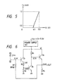
- an applied case of this circuit provides an advantage that the gain can be reduced stably. For example, if it is intended that the target gain is 32.5 dB, then I o ' is increased by 0.2 mA when V c is between 4.5 and 5.5 V as shown in Fig. 5. As a result,
- this system can freely adjust the gain isolating itself from or according to external variations (temperature, power supply voltage, or the like). To operate the system, it is only dc circuits that adjustments are needed; devices admitting ac signals can be left intact. Thus, it is also possible to externally control the gain of an amplifier.
- the photodiode produces a photoelectric current I PD according to a light signal.
- ac component of a potential at the base of Q1 is v0
- the ac component of v2 is V2
- the ac component of the output terminal is v out with the voltage gain of the amplifier stage is A
- circuit shown in Fig. 3 is suitable for a photodetection preamplifier for the following reason.
- the response bandwidth of the photodetection preamplifier is proportional to the gain, so that no signal can be transmitted if the bandwidth is too narrow; and if too wide, the response will be deteriorated by increased noise.
- the current supply I o ' is provided, the bandwidth can be maintained constant.
- the photodetection preamplifier will hereunder be described in comparison with a conventional power supply regulating system.
- Fig. 6 shows a conventional example.
- the anode of a photodiode (PD) whose cathode is biased is connected to a transistor Q1.
- the emitter of Q1 is grounded through a level shift diode D1, the base of Q2, and a resistor R E .
- the emitter of Q2 is grounded and its collector is connected to V c ' through its base and a resistor R1.
- the collectors of Q1 and Q3 are connected to a regulated power supply V c ' prepared by a regulated power supply circuit processing its input V c .
- the emitter of Q3 is connected to an output terminal, GND through a resistor R3, and the base of Q1 through a feedback resistor R f .
- an emitter follower is provided before the amplification stage. If the ac component of the base of Q2 is v0, and the ac component of the base of Q2 is v i , the following can be obtained since the voltage gain of the emitter follower is substantially 1.
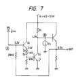
- Fig. 7 shows an embodiment according to this invention. It differs from the embodiment of Fig. 6 in that the current supply I o ' is connected to the collector of Q2; the collectors of Q1 and Q3 and the resistor R1 are connected directly to the power supply V c ; and a diode D2 is additionally inserted in parallel with the level shift diode D1 because the power supply voltage to be applied to the amplifier is high.
- a bandwidth f c ampler than that of the conventional system can be obtained. Since the maximum allowable current is also much ampler than that of the conventional system shown in Fig. 6.
- this system allows the application of high power supply voltages to the amplifier, thereby providing advantages in design.
Abstract
A gain stabilizing amplifier comprises an amplifying transistor (Q₁) for amplifying an input signal; a node (B) for determining a current flowing into the amplifying transistor (Q₁); a variable current supply (Io) connected to the node (B), a current output from the variable current supply (Io) being set to offset variations in a bias current of the amplifying transistor (Q₁).
Description
- This invention relates to a gain stabilizing amplifier using a transistor.
- To stabilize the gain of an amplifier in response to power supply variations and environmental changes, techniques of providing a circuit such as
- (1) a feedback circuit; and
- (2) a constant voltage power circuit have heretofore been employed.
- However, the technique (1) above presents the problem of not being suitable for use in high impedance amplifiers because the input impedance of the amplifier is reduced.
- On the other hand, the above technique (2) has a shortcoming that the power supply voltage which is applied effectively to the amplifier circuit is decreased. For example, in an amplifier to which a voltage of + 5 V is externally supplied, a built-in power supply circuit reduces that voltage to stabilize it. Therefore, the voltage actually applied to the amplifying transistor is about + 4 V. In order to avoid such a voltage drop, a booster circuit is required, and this increases the size of the circuit to a great extent.
- In view of the above problems, an object of the present invention is to provide an amplifier capable of stabilizing its gain without causing negative effects on the characteristics inherent in the amplifier such as input impedance reduction nor complicating the circuit configuration.
- To achieve the above object, the present invention provides, in an amplifier using a transistor, a gain stabilizing amplifier wherein a variable current supply is connected to a node for determining a bias current flowing to an amplifying transistor and an output current of the variable current supply is adjusted so that bias current variations of the amplifying transistor will be offset.
- According to the present invention, in order to maintain the potential of a node that serves to determine a bias current flowing into the amplifying transistor at a prescribed value even in the case where the bias current value is varied with power supply variations and external environmental changes and as a result the gain is induced to change, a current supply is connected to the node, thereby reducing the bias current variation.
-
- Fig. 1 is a circuit diagram showing a first embodiment of the present invention;
- Fig. 2 is a diagram showing the output characteristic of a current supply Io shown in Fig. 1;
- Fig. 3 is a circuit diagram showing a second embodiment of the present invention;
- Fig. 4 is a diagram showing the output characteristic of a current supply Io' shown in Fig. 2;
- Fig. 5 is a diagram showing the output characteristic of a current supply according to an applied case of this invention;
- Fig. 6 is a circuit diagram showing a conventional example; and
- Fig. 7 is a circuit diagram according to the present invention, which is compared with the circuit of Fig. 6.
- The present invention will be described in detail with reference to embodiments.
- Fig. 1 is a circuit diagram showing a first embodiment of the present invention. In this embodiment a variable current supply Io is connected to the emitter of a transistor Q₁ constituting a conventional transistor amplifier, so that a potential at the emitter is maintained constant. It is assumed that the variable current supply Io exhibits the output characteristic shown in Fig. 2.
- In Fig. 1, a node A connected to an input terminal IN is biased by being connected to a power supply Vc through a resistor R₁ and to the ground through a resistor R₂, respectively. Further, the node A is connected to the base of an amplifying transistor Q₁. A node C of the collector of the transistor Q₁ is not only connected to the power supply Vc through a resistor Rc but also to the base of the transistor Q₂. The collector of the transistor Q₂ is also connected to the power supply Vc, and a node D of its emitter is grounded through an output terminal OUT and a resistor R₃. A node B of the emitter of Q₁ is grounded through a resistor RE. A capacitor C₁ is inserted between the node B and the ground, while the current supply Io is provided between the node B and the power supply Vc. In this embodiment, the bias current I flowing through the amplifying transistor Q₁ is determined by a voltage V₁ of the node B, the resistor RE, and the current supply Io and is given by the following equation.

- The amplifier of this type receives only an AC signal admitted through a capacitor at its input. The AC signal applied to the node A is subjected to voltage amplification by the transistor Q1, and then transmitted to the output terminal with the transistor Q2 as an output buffer.
- An operation of the embodiment shown in Fig. 1 will now be described.
- If there is no current supply Io, a gain A is determined by a bias current I that flows through a transistor Q₁, and it is expressed as follows.

where e is the elementary electric charge; k is the Boltzmann constant; and VBE is the base-to-emitter voltage. - In the above equation (1), if it is supposed that Vc (power supply voltage) = 5 V, R₁ = 32 KΩ, R₂ = 18 KΩ, VBE = 0.8 V, RE = 1 KΩ, and Rc = 1 KΩ, then the gain varies as great as 45 to 31.5 times with respect to a Vc variation of ± 0.5 V. However, if the current supply Io varies as shown in Fig. 2, the gain does not vary with the varying Vc.
- This means that the gain is determined by the bias current I flowing through the transistor Q₁. However, if there is no current supply Io, the gain is determined by the potential V₁ at the emitter of the transistor Q₁, since V₁ is affected by Vc variations. Thus, if the current supply Io is connected to the emitter as in the case of this embodiment, Io serves to compensate for the bias current I flowing through the transistor Q1 determined by V₁, thereby causing no gain variations with respect to variations of the power supply voltage Vc.
- In the embodiment shown in Fig. 1, the bias current I flowing through the transistor Q₁ is determined by the potential at the emitter, so that the current supply Io is connected to the emitter. However, if the bias current I is determined by the collector voltage as shown in Fig. 3, the current supply may be connected to the collector. The same applies to FETs.
- Now, since the output impedance of the current supply is very high, there will be no detrimental effects to ac operations. If the capacity of the current supply affects the amplifier circuit characteristics, a resistor may be inserted between the node determining the bias current of the amplifying transistor and the current supply.
- The current supply Io or Io' can set the gain of the transistor so that not only the power supply voltage variations but also temperature variations may be compensated for, thereby allowing an amplifier having predetermined gains within a wide range to be provided.
- Another embodiment will be described referring to Figs. 3 and 4.
- Fig. 3 shows a photodetection preamplifier. The anode of a photodiode, whose cathode is biased, is connected to the base of an amplifying transistor Q₁ and the emitter of Q₁ is grounded. The collector of Q₁ is connected to the base of an output transistor Q₂ and to a current supply Io', and further to a power supply Vc through a resistor Rc. The collector of Q₂ is connected to the power supply Vc and its emitter to an output terminal. Further, the emitter of Q₂ is connected to level shift diodes D₁ and D₂, one output of which is grounded through a resistor R₃ and the other connected to the base of Q₁ through a feedback resistor Rf. The bandwidth fc of this preamplifier can be given as follows.

where - A:
- gain
- R:
- Rf // {A x (Q₁ input resistance)}
- C:
- total capacitance at the base node of Q₁

- VBE:
- voltage between the base and emitter of the transistor
- Since redundant bandwidth contributes only to increasing noise, the following relationship must be satisfied to make fc constant when Vc = 5.0 ± 0.5 V.

If Rc = 1 KΩ, the solution is what is obtained by Fig. 4. Hence, the gain is given by
If VBE = 0.8 V and vT = 26 mV, then A = 34 dB. - Further, an applied case of this circuit provides an advantage that the gain can be reduced stably. For example, if it is intended that the target gain is 32.5 dB, then Io' is increased by 0.2 mA when Vc is between 4.5 and 5.5 V as shown in Fig. 5. As a result,

- If VBE = 0.8 V and vT = 26 mV, then A is stabilized at 32.5 dB.
- Although the above describes only the Vc variations, actually the resistor Rc, vT and VBE have their temperature characteristics. Therefore, Io' should be adjusted in consideration of these factors.
- The gain can be stabilized not only at a predetermined value but also according to an aimed characteristic. For example, if the target characteristic of an amplifier is 32 dB with Vc = 5.5 V, T = 0°C or 32.5 dB with Vc = 4.5 V, T = 70°C in relation to the downstream circuits, Io should be adjusted so that these conditions can be satisfied.
- Accordingly, this system can freely adjust the gain isolating itself from or according to external variations (temperature, power supply voltage, or the like). To operate the system, it is only dc circuits that adjustments are needed; devices admitting ac signals can be left intact. Thus, it is also possible to externally control the gain of an amplifier.
- The operation of the circuit shown in Fig. 3 will be described.
- The photodiode produces a photoelectric current IPD according to a light signal. In Fig. 3, if the ac component of a potential at the base of Q₁ is v₀, the ac component of v₂ is V₂, and the ac component of the output terminal is vout with the voltage gain of the amplifier stage is A,

- Rin:
- transistor input resistance
- In particular, the circuit shown in Fig. 3 is suitable for a photodetection preamplifier for the following reason.
- The response bandwidth of the photodetection preamplifier is proportional to the gain, so that no signal can be transmitted if the bandwidth is too narrow; and if too wide, the response will be deteriorated by increased noise. To this end, if there is no current supply Io' as shown in Fig. 3, the gain varies to a great extent responsive to a variation of Vc = + 5 V ± 0.5 V with a resultant bandwidth deviation of - 31% to + 91% from the set point. However, if the current supply Io' is provided, the bandwidth can be maintained constant.
- The photodetection preamplifier will hereunder be described in comparison with a conventional power supply regulating system.
- Fig. 6 shows a conventional example. The anode of a photodiode (PD) whose cathode is biased is connected to a transistor Q₁. The emitter of Q₁ is grounded through a level shift diode D₁, the base of Q₂, and a resistor RE. The emitter of Q₂ is grounded and its collector is connected to Vc' through its base and a resistor R₁. The collectors of Q₁ and Q₃ are connected to a regulated power supply Vc' prepared by a regulated power supply circuit processing its input Vc. The emitter of Q3 is connected to an output terminal, GND through a resistor R₃, and the base of Q₁ through a feedback resistor Rf. Normally, Vc' is about 3.5 V when Vc = 4.5 to 5.5 V. Let us now think about the maximum allowable value IPD.MAX of the current IPD flowing through the PD and the bandwidth fc, which is given by the following equation as previously described.

If C = 3 pF and R = 20 KΩ, then the bandwidth becomes
If the bandwidth to be obtained is about 50 MHz, the bandwidth fc must be increased at the sacrifice of the noise characteristic (reducing R). If it is otherwise possible that the transistor Q₂ can operate at high frequencies up to VCE = 1.0 V, the maximum allowable input will be about
- The operation of the circuit shown in Fig. 6 will be described.
- In Fig. 6, in order to make the maximum input current larger than that of the embodiment shown in Fig. 3, an emitter follower is provided before the amplification stage. If the ac component of the base of Q₂ is v₀, and the ac component of the base of Q₂ is vi, the following can be obtained since the voltage gain of the emitter follower is substantially 1.

- Thus, the operation is the same as that of the embodiment shown in Fig. 3.
- On the other hand, Fig. 7 shows an embodiment according to this invention. It differs from the embodiment of Fig. 6 in that the current supply Io' is connected to the collector of Q₂; the collectors of Q₁ and Q₃ and the resistor R₁ are connected directly to the power supply Vc; and a diode D₂ is additionally inserted in parallel with the level shift diode D₁ because the power supply voltage to be applied to the amplifier is high. In this case,

a bandwidth fc ampler than that of the conventional system can be obtained. Since
the maximum allowable current is also much ampler than that of the conventional system shown in Fig. 6. - Thus, this system allows the application of high power supply voltages to the amplifier, thereby providing advantages in design.
- As described in the foregoing pages, a simple construction achieved with an additional current supply makes it possible to maintain the gain constant even with respect to variations in power supply voltage and external environment. This allows other applications (e.g., photodetector) of the invention at low costs.

That is, the input resistor Rin and the feedback resistor Rf are used as the detection resistors for current-voltage conversion. Thus, the photocurrent IPD is converted to the voltage signal vout. If the gain A and the input resistance Rin are sufficiently large, the conversion gain Z will be as follows.

Claims (4)
- A gain stabilizing amplifier, comprising:
an amplifying transistor for amplifying an input signal;
a node for determining a current flowing into said amplifying transistor;
a variable current supply connected to said node, a current output from said variable current supply being set to offset variations in a bias current of said amplifying transistor. - A gain stabilizing amplifier as claimed in claim 1, wherein said input signal comprises an ac voltage.
- A gain stabilizing amplifier as claimed in claim 1, further comprising a photodiode for producing as said input signal a photoelectric current according to a light signal.
- A gain stbilizing amplifier as claimed in claim 1, further comprising a resistor inserted between said node and said variable current supply.
Priority Applications (2)
| Application Number | Priority Date | Filing Date | Title |
|---|---|---|---|
| EP90110886A EP0460273A1 (en) | 1990-06-08 | 1990-06-08 | Gain stabilizing amplifier |
| US07/535,587 US5087892A (en) | 1990-06-08 | 1990-06-11 | Gain stabilizing amplifier |
Applications Claiming Priority (1)
| Application Number | Priority Date | Filing Date | Title |
|---|---|---|---|
| EP90110886A EP0460273A1 (en) | 1990-06-08 | 1990-06-08 | Gain stabilizing amplifier |
Publications (1)
| Publication Number | Publication Date |
|---|---|
| EP0460273A1 true EP0460273A1 (en) | 1991-12-11 |
Family
ID=8204074
Family Applications (1)
| Application Number | Title | Priority Date | Filing Date |
|---|---|---|---|
| EP90110886A Withdrawn EP0460273A1 (en) | 1990-06-08 | 1990-06-08 | Gain stabilizing amplifier |
Country Status (2)
| Country | Link |
|---|---|
| US (1) | US5087892A (en) |
| EP (1) | EP0460273A1 (en) |
Cited By (1)
| Publication number | Priority date | Publication date | Assignee | Title |
|---|---|---|---|---|
| WO2000052820A1 (en) * | 1999-03-03 | 2000-09-08 | Maxim Integrated Products, Inc. | Transimpedance amplifiers with improved gain-bandwidth product |
Families Citing this family (5)
| Publication number | Priority date | Publication date | Assignee | Title |
|---|---|---|---|---|
| US5498865A (en) * | 1994-12-16 | 1996-03-12 | Eastman Kodak Company | Photodiode amplifier circuit with improved sensitivity to high efficiency illumination |
| EP0818829A1 (en) * | 1996-07-12 | 1998-01-14 | Hitachi, Ltd. | Bipolar transistor and method of fabricating it |
| US6359517B1 (en) * | 2000-01-28 | 2002-03-19 | Integration Associates Incorporated | Photodiode transimpedance circuit |
| US6614312B1 (en) * | 2002-03-22 | 2003-09-02 | Agilent Technologies, Inc. | Low noise amplifier and imaging element using same |
| US7449958B1 (en) * | 2005-08-17 | 2008-11-11 | Marvell International Ltd. | Open loop DC control for a transimpedance feedback amplifier |
Citations (3)
| Publication number | Priority date | Publication date | Assignee | Title |
|---|---|---|---|---|
| US3872392A (en) * | 1972-07-26 | 1975-03-18 | Hitachi Ltd | Cascade direct-coupled amplifier |
| US4122403A (en) * | 1977-06-13 | 1978-10-24 | Motorola, Inc. | Temperature stabilized common emitter amplifier |
| EP0067448A2 (en) * | 1981-06-16 | 1982-12-22 | Siemens Aktiengesellschaft | Optical receiving circuit |
Family Cites Families (2)
| Publication number | Priority date | Publication date | Assignee | Title |
|---|---|---|---|---|
| JPS528755A (en) * | 1975-07-10 | 1977-01-22 | Matsushita Electric Ind Co Ltd | Bias circuit |
| JPH0282804A (en) * | 1988-09-20 | 1990-03-23 | Mitsubishi Electric Corp | Preamplifier for optical reception |
-
1990
- 1990-06-08 EP EP90110886A patent/EP0460273A1/en not_active Withdrawn
- 1990-06-11 US US07/535,587 patent/US5087892A/en not_active Expired - Fee Related
Patent Citations (3)
| Publication number | Priority date | Publication date | Assignee | Title |
|---|---|---|---|---|
| US3872392A (en) * | 1972-07-26 | 1975-03-18 | Hitachi Ltd | Cascade direct-coupled amplifier |
| US4122403A (en) * | 1977-06-13 | 1978-10-24 | Motorola, Inc. | Temperature stabilized common emitter amplifier |
| EP0067448A2 (en) * | 1981-06-16 | 1982-12-22 | Siemens Aktiengesellschaft | Optical receiving circuit |
Non-Patent Citations (2)
| Title |
|---|
| PATENT ABSTRACTS OF JAPAN vol. 1, no. 72 (E-77)(696) 13 July 77, & JP-A-52 008755 (MATSUSHITA DENKI SANGYO K.K.) 22 January 1977 * |
| PATENT ABSTRACTS OF JAPAN vol. 2, no. 90 (E-78)(4133) 22 July 1978, & JP-A-53 054453 (TOKYO SHIBAURA DENKI K.K.) 17 May 1978 * |
Cited By (1)
| Publication number | Priority date | Publication date | Assignee | Title |
|---|---|---|---|---|
| WO2000052820A1 (en) * | 1999-03-03 | 2000-09-08 | Maxim Integrated Products, Inc. | Transimpedance amplifiers with improved gain-bandwidth product |
Also Published As
| Publication number | Publication date |
|---|---|
| US5087892A (en) | 1992-02-11 |
Similar Documents
| Publication | Publication Date | Title |
|---|---|---|
| US6643472B1 (en) | APD bias circuit | |
| US5455705A (en) | Transimpedance amplifier for optical receiver | |
| EP0181146A2 (en) | Transimpedance amplifier circuit | |
| US5793254A (en) | Monolithic amplifier with stable, high resistance feedback element and method for fabricating the same | |
| US6864751B1 (en) | Transimpedance amplifier with adjustable output amplitude and wide input dynamic-range | |
| US6031219A (en) | Bias voltage supply circuit for photoelectric converting element and photodetection circuit | |
| US3968361A (en) | Laser receiver anti-sun circuit | |
| US6323734B1 (en) | Trans-impedance amplifier | |
| US4492926A (en) | Amplitude modulation detector | |
| EP1062727A1 (en) | Gain control amplifier, variable gain amplifier and automatic gain control amplifier | |
| US4889985A (en) | Combined optical power meter and receiver | |
| JP2000504910A (en) | Method and apparatus for providing limited transimpedance amplification | |
| EP0460273A1 (en) | Gain stabilizing amplifier | |
| US5198658A (en) | Transimpedance amplifier-input stage for an optical receiver | |
| US20050175359A1 (en) | Optical receiver | |
| US6201446B1 (en) | Adaptive bandwidth stabilization for an integrated circuit amplifier | |
| US4642453A (en) | Apparatus for increasing the dynamic range in an integrating optoelectric receiver | |
| US5737111A (en) | Optical receiving apparatus | |
| US5304949A (en) | Common base amplifier | |
| US4593252A (en) | Enhanced transconductance amplifier | |
| JPH0282804A (en) | Preamplifier for optical reception | |
| US7317350B2 (en) | Transresistance amplifier for a charged particle detector | |
| JP3795626B2 (en) | Receiver circuit | |
| JP3106437B2 (en) | Optoelectronic integrated circuit device | |
| US3548291A (en) | Voltage regulator with a low input impedance and improved feedback gain characteristics |
Legal Events
| Date | Code | Title | Description |
|---|---|---|---|
| PUAI | Public reference made under article 153(3) epc to a published international application that has entered the european phase |
Free format text: ORIGINAL CODE: 0009012 |
|
| 17P | Request for examination filed |
Effective date: 19901220 |
|
| AK | Designated contracting states |
Kind code of ref document: A1 Designated state(s): DE FR GB |
|
| 17Q | First examination report despatched |
Effective date: 19940826 |
|
| STAA | Information on the status of an ep patent application or granted ep patent |
Free format text: STATUS: THE APPLICATION HAS BEEN WITHDRAWN |
|
| 18W | Application withdrawn |
Withdrawal date: 19960220 |