EP0458524B1 - An analog to digital converter - Google Patents
An analog to digital converter Download PDFInfo
- Publication number
- EP0458524B1 EP0458524B1 EP91304387A EP91304387A EP0458524B1 EP 0458524 B1 EP0458524 B1 EP 0458524B1 EP 91304387 A EP91304387 A EP 91304387A EP 91304387 A EP91304387 A EP 91304387A EP 0458524 B1 EP0458524 B1 EP 0458524B1
- Authority
- EP
- European Patent Office
- Prior art keywords
- analog
- digital
- integrators
- signal
- converter
- Prior art date
- Legal status (The legal status is an assumption and is not a legal conclusion. Google has not performed a legal analysis and makes no representation as to the accuracy of the status listed.)
- Expired - Lifetime
Links
Images


Classifications
-
- H—ELECTRICITY
- H03—ELECTRONIC CIRCUITRY
- H03M—CODING; DECODING; CODE CONVERSION IN GENERAL
- H03M3/00—Conversion of analogue values to or from differential modulation
- H03M3/30—Delta-sigma modulation
- H03M3/322—Continuously compensating for, or preventing, undesired influence of physical parameters
- H03M3/324—Continuously compensating for, or preventing, undesired influence of physical parameters characterised by means or methods for compensating or preventing more than one type of error at a time, e.g. by synchronisation or using a ratiometric arrangement
- H03M3/35—Continuously compensating for, or preventing, undesired influence of physical parameters characterised by means or methods for compensating or preventing more than one type of error at a time, e.g. by synchronisation or using a ratiometric arrangement using redundancy
-
- H—ELECTRICITY
- H03—ELECTRONIC CIRCUITRY
- H03M—CODING; DECODING; CODE CONVERSION IN GENERAL
- H03M3/00—Conversion of analogue values to or from differential modulation
- H03M3/30—Delta-sigma modulation
- H03M3/39—Structural details of delta-sigma modulators, e.g. incremental delta-sigma modulators
- H03M3/412—Structural details of delta-sigma modulators, e.g. incremental delta-sigma modulators characterised by the number of quantisers and their type and resolution
- H03M3/422—Structural details of delta-sigma modulators, e.g. incremental delta-sigma modulators characterised by the number of quantisers and their type and resolution having one quantiser only
- H03M3/43—Structural details of delta-sigma modulators, e.g. incremental delta-sigma modulators characterised by the number of quantisers and their type and resolution having one quantiser only the quantiser being a single bit one
-
- H—ELECTRICITY
- H03—ELECTRONIC CIRCUITRY
- H03M—CODING; DECODING; CODE CONVERSION IN GENERAL
- H03M3/00—Conversion of analogue values to or from differential modulation
- H03M3/30—Delta-sigma modulation
- H03M3/39—Structural details of delta-sigma modulators, e.g. incremental delta-sigma modulators
- H03M3/436—Structural details of delta-sigma modulators, e.g. incremental delta-sigma modulators characterised by the order of the loop filter, e.g. error feedback type
- H03M3/438—Structural details of delta-sigma modulators, e.g. incremental delta-sigma modulators characterised by the order of the loop filter, e.g. error feedback type the modulator having a higher order loop filter in the feedforward path
- H03M3/454—Structural details of delta-sigma modulators, e.g. incremental delta-sigma modulators characterised by the order of the loop filter, e.g. error feedback type the modulator having a higher order loop filter in the feedforward path with distributed feedback, i.e. with feedback paths from the quantiser output to more than one filter stage
Definitions
- the invention relates to analog to digital converters and more particularly to sigma-delta analog to digital converters.
- a converter of this type is known from the article by K. C-H Chac et al, "A higher order topology for interpolative modulators for oversampling A/D converters" in IEEE Transactions on Circuits and Systems, Vol. 37, No 3, March 1990, pages 309-318.
- Such converters comprise an analog modulator, the output of which is connected to a digital filter.
- the analog modulator includes a series of typically two or three analog integrators, although there may be only one or more than three.
- the analog modulator over-samples an incoming analog signal and generates a serial digital modulated signal at a frequency determined by the over-sampling clock frequency. This is both fed to the digital filter, and is used for negative feedback in the analog modulator.
- the modulated signal is processed by the digital filter which eliminates high frequency components to generate a parallel digital output signal at a lower rate.
- the digital filter is a separate processor which simply receives the modulated signal and carries out processing and storing functions to generate the digital output signal. Because the filter has a memory of previous inputs, there can be a delay of up to 0.1 second for the processing of an independent new input. Such a delay is of little consequence for applications such as a domestic stereo sound system. However, in some applications such as in multiplexing where there would be no relationship between different signals, such a delay is unacceptable because it leads to considerable delays in operation of the multiplexer. A further problem with presently available digital filters is that they are complex and expensive as they are designed to model or approximate the analog signal by removing the high frequency part of the modulated signal.
- the invention is directed towards providing a sigma-delta analog to digital converter to overcome these problems.
- a sigma-delta analog to digital converter comprising an analog modulator for generation of a digital modulated signal, the analog modulator comprising a plurality of analog integrators and a negative feedback loop, and a digital filter for generation of an output digital signal at a rate lower than the rate at which the analog modulator operates, characterised in that the analog modulator comprises a series of at least two analog integrators in a loop, each analog integrator has an associated reset circuit, and the digital filter comprises resettable filter means for replicating processing of the modulated signal by at least the first two analog integrators.
- the filter means comprises a plurality of digital integrators connected to replicate processing of the modulated signal by corresponding analog integrators. This is a simple and inexpensive construction.
- each analog integrator there is a digital integrator corresponding to each analog integrator. This provides for good accuracy.
- the output of the last analog integrator is connected to an auxiliary multi-bit analog to digital converter, the output of which is connected to an auxiliary digital integrator connected to the output of the last digital integrator. This provides for still further improved accuracy.
- the invention provides a method of carrying out single shot analog to digital conversion in a sigma-delta analog to digital converter comprising an analog modulator having a plurality of analog integrators in a loop, a comparator, and a feedback path; and a digital filter, the method comprising the steps of:-
- said step of over-sampling the input analog signal lasts for only a portion of the conversion cycle.
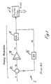
- Fig. 1 there is illustrated a typical first order sigma-delta analog to digital converter of the prior art.
- the converter comprises an analog modulator I connected to a digital filter II.
- the analog modulator I comprises a summing junction III connected to an analog integrator IV, the output of which is connected to an A/D converter V which provides a serial digital modulated signal.
- the modulated signal is fed back to a D/A converter VI which provides negative feedback into the summing junction III.
- the analog integrator IV acts as an accumulator, the output of which is converted to a reference voltage (typically +/-1V) resulting in a positive or a negative value for the modulated signal.
- the over-sampling frequency is determined by the clock frequency and the modulated signal is a one-bit data stream at this frequency.
- the digital filter II receives the modulated signal and carries out processing operations including storage of the signals to output a 16-bit digital output at regular intervals.
- the digital filter may receive a reset instruction from a controller, which instruction causes clearing of the memory so that it is ready to process for the next output. This typically causes a delay of approximately 0.1 second.
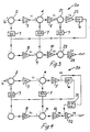
- the converter 1 is of the second order type and includes a reset circuit.
- the analog modulator comprises a first analog summing junction 2 connected to a first analog integrator 3 which is in turn connected to a second analog summing junction 4, the output of which feeds a second analog integrator 5.
- the analog integrators 3 and 5 are each of the switched capacitor type.
- the output of the second analog integrator 5 is connected to a comparator 6 which outputs a serial digital modulated signal at a bit rate corresponding to the over-sampling frequency, which digital signal is referred to as "comp”.
- the analog modulator is completed by a pair of D/A converters 7, each of which is connected for delivering a reference voltage of +/-V ref to the first and second analog summing junctions 2 and 4.
- the digital filter comprises a first digital integrator 8 connected to a digital summing junction 9, the output of which is connected to a second digital integrator 10.
- the comparator 6 output which provides the negative feedback for the analog modulator is connected directly to the first digital integrator 8 and is also connected to the input of the digital summing junction 9.
- the digital integrators 8 and 10 each include a reset circuit.
- the analog modulator over-samples the input analog signal X at a relatively high clock cycle rate say, 254 kHz.
- the modulated signal "comp” is fed back to the analog summing junctions 2 and 4 as a plus or minus negative feedback reference voltage V ref .
- the purpose of the feedback is to ensure that the outputs V1 and V2 of the analog integrators 3 and 5 are kept small.
- the gains k1 and k2 of the analog integrators are chosen to ensure that V1 and V2 are always less than + /- V ref .
- V1 and V2 are set to zero as are the outputs D1 and D2 of the digital integrators 8 and 10.
- D2 is a function of D1 and the negative feedback, "comp”.
- D1 is in turn a function of the negative feedback "comp”.
- the gains k1 and k2 are each chosen to be 0.5
- the equations (e) to (j) are derived from merging the equations (a) to (d).
- the input analog signal X can be equated to a known function of V2, D2, V ref , k1 and k2.
- D2 may be regarded as a digital representation of X with a maximum error of V2 divided by the denominator of equation (j).
- This error is derived from a sum of sums of a constant and for n steps, and thus n clock cycles, the sum of sums is n(n-1)/2.
- X is known to an accuracy of V2/[k1.k2(n-1)n]. For 12-bit accuracy 128 samples are required and for 16-bit accuracy 512 samples would be required.
- the input analog signal X is kept between +/-0.5 V and V ref is 1.0 V, for 128 samples the digital estimate of the input will have a maximum error of 0.246 mV.
- the digital filter replicates processing of the feedback signal by the analog modulator. Accordingly, the digital filter and the analog modulator work in synchronism (in parallel) and accordingly when reset instructions are simultaneously received from a controller both the analog modulator and the digital filter may be reset simultaneously by their reset circuits. This would occur once for each output signal, giving a conversion cycle and single shot operation. There is no delay between conversion cycles. This is particularly important where the input analog signal changes unpredictably and, in control applications where many different signals are being monitored with the aid, for example of a multiplexer.
- the feedback signal is a good representation of X and this is processed in the same manner as in the analog modulator, good accuracy is achieved.
- the digital filter is of simple construction and may be easily integrated onto an integrated circuit. This will considerably reduce manufacturing costs.
- the invention is not limited to the embodiment illustrated in Fig. 2.
- Fig. 3 there is illustrated an alternative construction of converter, indicated generally by the reference numeral 20. Parts similar to those described with reference to Fig. 2 are identified by the same reference numerals.
- the converter 20 is of the third order type including a third analog summing junction 21 and a third analog integrator 22.
- the digital filter includes a corresponding third digital summing junction 23 and a third digital integrator 24.
- the digital filter may replicate processing of the feedback signal so that it may be reset together with the analog modulator once per conversion cycle.
- the converter of the invention may be of any order, higher than single order.
- the converter 30 includes an auxiliary A/D converter 31 for 5-bit conversion.
- the converter 31 is connected at the output of the second analog integrator 5 for evaluation of V2 at the end of each conversion cycle.
- the residual caused by the presence of V2 in the integrator may be reduced by 5-bit calculation of the value of V2 at the end of the conversion cycle. This will allow an extra 4-bits of resolution of X and 16-bit conversion accuracy in 128 clock cycles.
- the converter 31 is connected to an auxiliary digital integrator 32 connected at the output of the second digital integrator 10, the digital output being D3. It will be appreciated that this arrangement provides for significantly improved accuracy.
- the invention may be applied to any type of sigma-delta converter, for example, referring to Fig. 5, there is illustrated an implementation of the invention with a sigma-delta analog to digital converter of the "feed forward" type. It will be seen from the equations given with Fig. 5 that the digital value D 2 is proportional to X to a good accuracy. Again, the digital integrators 8 and 9 mirror processing of the feedback signal "comp" by the analog integrators 3 and 5 and so when reset instructions are received they will simultaneously reset at the end of each conversion cycle.
- the invention is not limited to the embodiments hereinbefore described.
- the feedback signal of the analog modulator may be multi-bit instead of single bit.
- the digital filter may not include digital integrators. Instead, a processing circuit together with look-up tables may be used in order to replicate processing of the feedback signal by the analog integrators. It is envisaged that there are many ways in which this could be carried out in software.
- the important point of the invention is that the digital filter is resettable and replicates processing by the analog modulator of the feedback signal so that when reset instructions are received the analog modulator and the digital filter reset simultaneously. It is envisaged that the analog modulator may only sample for portion of the clock cycles in a conversion cycle, which may improve stability.
Abstract
Description
- The invention relates to analog to digital converters and more particularly to sigma-delta analog to digital converters.
- A converter of this type is known from the article by K. C-H Chac et al, "A higher order topology for interpolative modulators for oversampling A/D converters" in IEEE Transactions on Circuits and Systems, Vol. 37,
No 3, March 1990, pages 309-318. - Such converters comprise an analog modulator, the output of which is connected to a digital filter. The analog modulator includes a series of typically two or three analog integrators, although there may be only one or more than three. The analog modulator over-samples an incoming analog signal and generates a serial digital modulated signal at a frequency determined by the over-sampling clock frequency. This is both fed to the digital filter, and is used for negative feedback in the analog modulator. The modulated signal is processed by the digital filter which eliminates high frequency components to generate a parallel digital output signal at a lower rate.
- In presently available converters, the digital filter is a separate processor which simply receives the modulated signal and carries out processing and storing functions to generate the digital output signal. Because the filter has a memory of previous inputs, there can be a delay of up to 0.1 second for the processing of an independent new input. Such a delay is of little consequence for applications such as a domestic stereo sound system. However, in some applications such as in multiplexing where there would be no relationship between different signals, such a delay is unacceptable because it leads to considerable delays in operation of the multiplexer. A further problem with presently available digital filters is that they are complex and expensive as they are designed to model or approximate the analog signal by removing the high frequency part of the modulated signal.
- In the article entitled "A second-order high-resolution incremental AID converter with offset and charge injection compensation" by J. Robert and P Dival and published in IEEE Journal of Solid-State Circuits, Vol. 23, No. 3 June 1988, a sigma-delta AID converter is described. In order to achieve a higher-order, the analog modulator is cascaded with a number of loops, each having a single analog integrator. This is a complex arrangement, and inaccuracy could arise due to manufacturing differences in the loops.
- The invention is directed towards providing a sigma-delta analog to digital converter to overcome these problems.
- According to the invention there is provided a sigma-delta analog to digital converter comprising an analog modulator for generation of a digital modulated signal, the analog modulator comprising a plurality of analog integrators and a negative feedback loop, and a digital filter for generation of an output digital signal at a rate lower than the rate at which the analog modulator operates, characterised in that the analog modulator comprises a series of at least two analog integrators in a loop, each analog integrator has an associated reset circuit, and the digital filter comprises resettable filter means for replicating processing of the modulated signal by at least the first two analog integrators.
- Thus, when reset instructions are received simultaneously by both the analog modulator and the digital filter, they may reset together. Accordingly, there is no data storage in the digital filter and thus no delay in generating an output digital signal. Further because the modulated signal is a good representation of the analog signal, good accuracy is achieved.
- In one embodiment, the filter means comprises a plurality of digital integrators connected to replicate processing of the modulated signal by corresponding analog integrators. This is a simple and inexpensive construction.
- Preferably, there is a digital integrator corresponding to each analog integrator. This provides for good accuracy.
- In one embodiment, the output of the last analog integrator is connected to an auxiliary multi-bit analog to digital converter, the output of which is connected to an auxiliary digital integrator connected to the output of the last digital integrator. This provides for still further improved accuracy.
- According to another aspect, the invention provides a method of carrying out single shot analog to digital conversion in a sigma-delta analog to digital converter comprising an analog modulator having a plurality of analog integrators in a loop, a comparator, and a feedback path; and a digital filter, the method comprising the steps of:-
- simultaneously resetting the analog integrators and the digital filter;
- the analog integrators successively over-sampling an input analog signal in a serial manner to generate a filtered signal;
- the comparator subsequently comparing the filtered signal with a reference signal to provide a digital modulated signal;
- the feedback path inputting the digital modulated signal to the analog integrators via digital to analog converters, and to the digital filter;
- filtering the modulated signal at the digital filter in a manner which replicates processing of said signal by at least the first two analog integrators; and
- outputting a digital signal from the digital filter at the end of a conversion cycle which comprises a fixed number of clock cycles.
- In one embodiment, said step of over-sampling the input analog signal lasts for only a portion of the conversion cycle.
- The invention will be more clearly understood from the following description of some preferred embodiments thereof, given by way of example only with reference only to the accompanying drawings in which:-
- Fig. 1
- is a diagram of a sigma-delta analog to digital converter of the prior art;
- Fig. 2
- is a diagram of a converter of the invention, together with equations illustrating operation of the converter; and
- Figs. 3, 4 and 5
- are diagrams showing various alternative constructions of converter of the invention.
- Referring to the drawings, and initially to Fig. 1 there is illustrated a typical first order sigma-delta analog to digital converter of the prior art. The converter comprises an analog modulator I connected to a digital filter II. The analog modulator I comprises a summing junction III connected to an analog integrator IV, the output of which is connected to an A/D converter V which provides a serial digital modulated signal. The modulated signal is fed back to a D/A converter VI which provides negative feedback into the summing junction III.
- In operation, the analog integrator IV acts as an accumulator, the output of which is converted to a reference voltage (typically +/-1V) resulting in a positive or a negative value for the modulated signal. The over-sampling frequency is determined by the clock frequency and the modulated signal is a one-bit data stream at this frequency. The digital filter II receives the modulated signal and carries out processing operations including storage of the signals to output a 16-bit digital output at regular intervals. The digital filter may receive a reset instruction from a controller, which instruction causes clearing of the memory so that it is ready to process for the next output. This typically causes a delay of approximately 0.1 second.
- Referring now to Fig. 2, there is illustrated a sigma-delta analog to digital converter of the invention, indicated generally by the
reference numeral 1. Theconverter 1 is of the second order type and includes a reset circuit. The analog modulator comprises a firstanalog summing junction 2 connected to a firstanalog integrator 3 which is in turn connected to a secondanalog summing junction 4, the output of which feeds a secondanalog integrator 5. Theanalog integrators analog integrator 5 is connected to a comparator 6 which outputs a serial digital modulated signal at a bit rate corresponding to the over-sampling frequency, which digital signal is referred to as "comp". The analog modulator is completed by a pair of D/A converters 7, each of which is connected for delivering a reference voltage of +/-Vref to the first and secondanalog summing junctions digital integrator 8 connected to adigital summing junction 9, the output of which is connected to a seconddigital integrator 10. The comparator 6 output which provides the negative feedback for the analog modulator is connected directly to the firstdigital integrator 8 and is also connected to the input of thedigital summing junction 9. Thedigital integrators - In operation, the analog modulator over-samples the input analog signal X at a relatively high clock cycle rate say, 254 kHz. The modulated signal "comp" is fed back to the
analog summing junctions analog integrators - At the start of conversion, V1 and V2 are set to zero as are the outputs D1 and D2 of the
digital integrators converter 1 is of the second order type, the gains k1 and k2 are each chosen to be 0.5 The equations (e) to (j) are derived from merging the equations (a) to (d). As will be seen in equation (j) the input analog signal X can be equated to a known function of V2, D2, Vref, k1 and k2. As V2 is within the range of +/- Vref, this can be ignored and D2 may be regarded as a digital representation of X with a maximum error of V2 divided by the denominator of equation (j). This error is derived from a sum of sums of a constant and for n steps, and thus n clock cycles, the sum of sums is n(n-1)/2. Thus, for any clock cycle n, X is known to an accuracy of V2/[k1.k2(n-1)n]. For 12-bit accuracy 128 samples are required and for 16-bit accuracy 512 samples would be required. - If for example, the input analog signal X is kept between +/-0.5 V and Vref is 1.0 V, for 128 samples the digital estimate of the input will have a maximum error of 0.246 mV.
- It will be appreciated that because of use of the
digital integrators analog integrators - The invention is not limited to the embodiment illustrated in Fig. 2. For example, referring now to Fig. 3 there is illustrated an alternative construction of converter, indicated generally by the
reference numeral 20. Parts similar to those described with reference to Fig. 2 are identified by the same reference numerals. Theconverter 20 is of the third order type including a thirdanalog summing junction 21 and athird analog integrator 22. The digital filter includes a corresponding third digital summingjunction 23 and a thirddigital integrator 24. Thus, again the digital filter may replicate processing of the feedback signal so that it may be reset together with the analog modulator once per conversion cycle. Needless to say, the converter of the invention may be of any order, higher than single order. It has been found that if processing of the feedback signal in only some of the analog integrators beginning with the first two is replicated in the digital filter, single shot operation is still achieved, although accuracy is disimproved. Accordingly, it is not necessary that there be a digital integrator corresponding to each analog integrator, however, this is the preferred construction. - Referring now to Fig. 4 there is illustrated an alternative second order converter of the invention, indicated generally by the
reference numeral 30. Again, parts similar to those described with reference to the previous drawings are identified by the same reference numerals. Theconverter 30 includes an auxiliary A/D converter 31 for 5-bit conversion. Theconverter 31 is connected at the output of thesecond analog integrator 5 for evaluation of V2 at the end of each conversion cycle. Referring again to equation (j), the residual caused by the presence of V2 in the integrator may be reduced by 5-bit calculation of the value of V2 at the end of the conversion cycle. This will allow an extra 4-bits of resolution of X and 16-bit conversion accuracy in 128 clock cycles. Theconverter 31 is connected to an auxiliarydigital integrator 32 connected at the output of the seconddigital integrator 10, the digital output being D3. It will be appreciated that this arrangement provides for significantly improved accuracy. - The invention may be applied to any type of sigma-delta converter, for example, referring to Fig. 5, there is illustrated an implementation of the invention with a sigma-delta analog to digital converter of the "feed forward" type. It will be seen from the equations given with Fig. 5 that the digital value D2 is proportional to X to a good accuracy. Again, the
digital integrators analog integrators - The invention is not limited to the embodiments hereinbefore described. For example, it is envisaged that the feedback signal of the analog modulator may be multi-bit instead of single bit. It is also envisaged that the digital filter may not include digital integrators. Instead, a processing circuit together with look-up tables may be used in order to replicate processing of the feedback signal by the analog integrators. It is envisaged that there are many ways in which this could be carried out in software. The important point of the invention is that the digital filter is resettable and replicates processing by the analog modulator of the feedback signal so that when reset instructions are received the analog modulator and the digital filter reset simultaneously. It is envisaged that the analog modulator may only sample for portion of the clock cycles in a conversion cycle, which may improve stability.
Claims (6)
- A sigma-delta analog to digital converter (1) comprising an analog modulator for generation of a digital modulated signal (comp), the analog modulator comprising a plurality of analog integrators (3,5) and a negative feedback loop (7), and a digital filter for generation of an output digital signal (D2) at a rate lower than the rate at which the analog modulator operates , characterised in that the analog modulator comprises a series of at least two analog integrators in a loop, each analog integrator (3,5) has a reset circuit, and the digital filter comprises resettable filter means (8,10) for replicating processing of the modulated signal (comp) by at least the first two analog integrators (3).
- A converter as claimed in claim 1 wherein the filter means comprises a plurality of digital integrators (8,10) connected to replicate processing of the modulated signal by corresponding analog integrators (3,5).
- A converter as claimed in claim 2 wherein there is a digital integrator (8,10) corresponding to each analog integrator (3,5).
- A converter as claimed in claims 2 or 3, wherein the output of the last analog integrator is connected to an auxiliary multi-bit analog to digital converter (31), the output of which is connected to an auxiliary digital integrator (32) connected to the output of the last digital integrator (10).
- A method of carrying out single shot analog to digital conversion in a sigma-delta analog to digital converter comprising an analog modulator having a plurality of analog integrators in a loop, a comparator, and a feedback path; and a digital filter; the method comprising the steps of:-simultaneously resetting the analog integrators (3, 5) and the digital filter (8, 9, 10);the analog integrators (3, 5) successively over-sampling an input analog signal in a serial manner to generate a filtered signal (V2);the comparator (6) subsequently comparing the filtered signal (V2) with a reference signal to provide a digital modulated signal (comp);the feedback path inputting the digital modulated signal to the analog integrators via digital to analog converters (7), and to the digital filter;filtering the modulated signal (comp) at the digital filter in a manner which replicates processing of said signal by at least the first two analog integrators (3, 5); andoutputting a digital signal from the digital filter at the end of a conversion cycle which comprises a fixed number of clock cycles.
- A method as claimed in claim 5, wherein said step of over-sampling the input analog signal lasts for only a portion of the conversion cycle.
Applications Claiming Priority (2)
| Application Number | Priority Date | Filing Date | Title |
|---|---|---|---|
| IE181590 | 1990-05-21 | ||
| IE181590A IE901815A1 (en) | 1990-05-21 | 1990-05-21 | An analog to digital converter |
Publications (3)
| Publication Number | Publication Date |
|---|---|
| EP0458524A2 EP0458524A2 (en) | 1991-11-27 |
| EP0458524A3 EP0458524A3 (en) | 1993-08-11 |
| EP0458524B1 true EP0458524B1 (en) | 1996-12-04 |
Family
ID=11031082
Family Applications (1)
| Application Number | Title | Priority Date | Filing Date |
|---|---|---|---|
| EP91304387A Expired - Lifetime EP0458524B1 (en) | 1990-05-21 | 1991-05-16 | An analog to digital converter |
Country Status (7)
| Country | Link |
|---|---|
| US (1) | US5189419A (en) |
| EP (1) | EP0458524B1 (en) |
| JP (1) | JPH0613905A (en) |
| AT (1) | ATE146022T1 (en) |
| CA (1) | CA2042821C (en) |
| DE (1) | DE69123388T2 (en) |
| IE (1) | IE901815A1 (en) |
Families Citing this family (26)
| Publication number | Priority date | Publication date | Assignee | Title |
|---|---|---|---|---|
| DE59205500D1 (en) * | 1992-03-12 | 1996-04-04 | Siemens Ag | Sigma delta modulator |
| EP0602718B1 (en) * | 1992-12-16 | 1998-08-19 | Koninklijke Philips Electronics N.V. | Analog-to-digital converter for converting a multitude of analog input signals into digital output signals by means of one sigma-delta modulator |
| US5345236A (en) * | 1992-12-21 | 1994-09-06 | Harris Corporation | Improved sigma-delta type analog-to-digital converter and method |
| SE502900C2 (en) * | 1994-11-01 | 1996-02-19 | Foersvarets Forskningsanstalt | Analog-to-digital converter and sensor device including such |
| US5621675A (en) * | 1994-11-02 | 1997-04-15 | Advanced Micro Devices, Inc. | Digital decimation and compensation filter system |
| US5646621A (en) * | 1994-11-02 | 1997-07-08 | Advanced Micro Devices, Inc. | Delta-sigma ADC with multi-stage decimation filter and gain compensation filter |
| US5648779A (en) * | 1994-12-09 | 1997-07-15 | Advanced Micro Devices, Inc. | Sigma-delta modulator having reduced delay from input to output |
| US5617090A (en) * | 1995-05-10 | 1997-04-01 | Harris Corporation | Multi-channel sigma-delta A/D converters with improved throughput |
| US5751615A (en) * | 1995-11-14 | 1998-05-12 | Advanced Micro Devices, Inc. | Implementation of a digital decimation filter and method |
| US5732004A (en) * | 1995-11-14 | 1998-03-24 | Advanced Micro Devices, Inc. | DSP architecture for a FIR-type filter and method |
| DE19630052A1 (en) * | 1996-07-25 | 1997-07-10 | Siemens Ag | Digital=analogue converter using sigma-delta method |
| US6205219B1 (en) * | 1998-02-24 | 2001-03-20 | Lucent Technologies, Inc. | Call related information reception using sigma/delta modulation |
| US6208279B1 (en) * | 1998-08-17 | 2001-03-27 | Linear Technology Dorporation | Single-cycle oversampling analog-to-digital converter |
| JP3407871B2 (en) * | 1999-09-17 | 2003-05-19 | 日本電気株式会社 | Analog / digital mixed ΔΣ modulator |
| US6744394B2 (en) * | 2002-05-10 | 2004-06-01 | 02Micro International Limited | High precision analog to digital converter |
| JP5100446B2 (en) * | 2008-02-28 | 2012-12-19 | 東光東芝メーターシステムズ株式会社 | Electricity meter |
| JP5153385B2 (en) * | 2008-02-28 | 2013-02-27 | 東光東芝メーターシステムズ株式会社 | Electricity meter |
| EP2877462B1 (en) * | 2012-07-27 | 2019-09-04 | Celgene Corporation | Processes for preparing isoindoline-1,3-dione compounds |
| JP5915669B2 (en) | 2014-01-14 | 2016-05-11 | 株式会社デンソー | A / D converter |
| JP6436022B2 (en) | 2015-09-03 | 2018-12-12 | 株式会社デンソー | A / D converter |
| US9806552B2 (en) | 2016-02-15 | 2017-10-31 | Analog Devices Global | Analog/digital converter with charge rebalanced integrator |
| US10123384B1 (en) | 2017-09-22 | 2018-11-06 | Linear Technology Holding, LLC | LED dimming |
| US10201052B1 (en) | 2017-09-22 | 2019-02-05 | Linear Technology Holding, LLC | LED dimming |
| US10136488B1 (en) * | 2017-10-05 | 2018-11-20 | Linear Technology Holding, LLC | LED dimming |
| CN112097902B (en) | 2019-12-03 | 2023-08-11 | 义明科技股份有限公司 | Optical sensor and sensing method thereof |
| TWI746067B (en) * | 2019-12-03 | 2021-11-11 | 義明科技股份有限公司 | Light sensor and sensing method thereof |
Family Cites Families (6)
| Publication number | Priority date | Publication date | Assignee | Title |
|---|---|---|---|---|
| US4616349A (en) * | 1982-11-22 | 1986-10-07 | Mobil Oil Corporation | Analog-to-digital converter for seismic exploration using delta modulation |
| US4692719A (en) * | 1986-08-01 | 1987-09-08 | Telectronics N.V. | Combined pacemaker delta modulator and bandpass filter |
| US4851841A (en) * | 1987-10-02 | 1989-07-25 | Crystal Semiconductor Corporation | Gain scaling of oversampled analog-to-digital converters |
| JP2650711B2 (en) * | 1988-03-25 | 1997-09-03 | 株式会社日立製作所 | Oversampling A / D converter |
| US5028924A (en) * | 1990-03-02 | 1991-07-02 | Motorola, Inc. | Digital correction of gain mismatch in a sigma delta modulator |
| US4999625A (en) * | 1990-03-02 | 1991-03-12 | Motorola, Inc. | Generation of a digital correction signal to compensate for gain mismatches in a sigma delta modulator |
-
1990
- 1990-05-21 IE IE181590A patent/IE901815A1/en not_active IP Right Cessation
-
1991
- 1991-05-16 AT AT91304387T patent/ATE146022T1/en not_active IP Right Cessation
- 1991-05-16 DE DE69123388T patent/DE69123388T2/en not_active Expired - Fee Related
- 1991-05-16 EP EP91304387A patent/EP0458524B1/en not_active Expired - Lifetime
- 1991-05-17 CA CA002042821A patent/CA2042821C/en not_active Expired - Fee Related
- 1991-05-20 US US07/702,337 patent/US5189419A/en not_active Expired - Lifetime
- 1991-05-21 JP JP3228234A patent/JPH0613905A/en active Pending
Non-Patent Citations (2)
| Title |
|---|
| IEEE JOURNAL OF SOLID-STATE CIRCUITS vol. 22, no. 2, April 1987, pages 157-163, ROBERT ET AL, 'A 16-bit Low-Voltage CMOS A/D Converter' * |
| IEEE JOURNAL OF SOLID-STATE CIRCUITS vol. 23, no. 3, June 1988, pages 736-741, ROBERT ET AL, 'A Second-Order High-Resolution Incremental A/D Converter with Offset and Charge Injection Compensation' * |
Also Published As
| Publication number | Publication date |
|---|---|
| CA2042821A1 (en) | 1991-11-22 |
| DE69123388D1 (en) | 1997-01-16 |
| DE69123388T2 (en) | 1997-05-15 |
| JPH0613905A (en) | 1994-01-21 |
| IE901815A1 (en) | 1991-12-04 |
| EP0458524A3 (en) | 1993-08-11 |
| CA2042821C (en) | 1997-03-18 |
| ATE146022T1 (en) | 1996-12-15 |
| EP0458524A2 (en) | 1991-11-27 |
| US5189419A (en) | 1993-02-23 |
Similar Documents
| Publication | Publication Date | Title |
|---|---|---|
| EP0458524B1 (en) | An analog to digital converter | |
| US5055843A (en) | Sigma delta modulator with distributed prefiltering and feedback | |
| US5103229A (en) | Plural-order sigma-delta analog-to-digital converters using both single-bit and multiple-bit quantization | |
| US5682161A (en) | High-order delta sigma modulator | |
| US5241310A (en) | Wide dynamic range delta sigma analog-to-digital converter with precise gain tracking | |
| EP0368610B1 (en) | A method of cascading two or more sigma-delta modulators and a sigma-delta modulator system | |
| EP0796525B1 (en) | Sigma-delta modulator with reduced delay from input to output | |
| EP0513241A1 (en) | Sigma delta modulator. | |
| JPH01305725A (en) | Digital/analog converter | |
| JPH01284110A (en) | Serial bit device | |
| JPH0779243B2 (en) | Oversample type A / D converter | |
| GB2080059A (en) | Digital-to-analogue converter | |
| US6762707B2 (en) | Programmable architecture analog-to-digital converter | |
| JPH04302222A (en) | Sigma delta type d/a converter system | |
| JPH07105762B2 (en) | Analog-to-digital converter using decimation filter of sigma-delta converter and the same | |
| US4987416A (en) | Analog to digital converters | |
| US5287106A (en) | Circuit for PCM conversion of an analog signal, with improvement in gain-tracking | |
| US7782239B2 (en) | Multi-stage resettable sigma-delta converters | |
| JP3161481B2 (en) | Offset compensation circuit for interleaved A / D converter | |
| JPS6313520A (en) | Analog-digital conversion circuit | |
| CA1240798A (en) | Sampling rate converter for delta modulated signals | |
| US4899155A (en) | Apparatus and method for analogue to digital conversion | |
| JP2874218B2 (en) | A / D converter | |
| EP0289082A1 (en) | Digital-to-analog converter | |
| JP3232865B2 (en) | Digital / analog signal converter |
Legal Events
| Date | Code | Title | Description |
|---|---|---|---|
| PUAI | Public reference made under article 153(3) epc to a published international application that has entered the european phase |
Free format text: ORIGINAL CODE: 0009012 |
|
| AK | Designated contracting states |
Kind code of ref document: A2 Designated state(s): AT BE CH DE DK ES FR GB GR IT LI LU NL SE |
|
| 17P | Request for examination filed |
Effective date: 19920520 |
|
| PUAL | Search report despatched |
Free format text: ORIGINAL CODE: 0009013 |
|
| AK | Designated contracting states |
Kind code of ref document: A3 Designated state(s): AT BE CH DE DK ES FR GB GR IT LI LU NL SE |
|
| GRAG | Despatch of communication of intention to grant |
Free format text: ORIGINAL CODE: EPIDOS AGRA |
|
| GRAG | Despatch of communication of intention to grant |
Free format text: ORIGINAL CODE: EPIDOS AGRA |
|
| 17Q | First examination report despatched |
Effective date: 19960117 |
|
| GRAH | Despatch of communication of intention to grant a patent |
Free format text: ORIGINAL CODE: EPIDOS IGRA |
|
| GRAH | Despatch of communication of intention to grant a patent |
Free format text: ORIGINAL CODE: EPIDOS IGRA |
|
| GRAG | Despatch of communication of intention to grant |
Free format text: ORIGINAL CODE: EPIDOS AGRA |
|
| GRAA | (expected) grant |
Free format text: ORIGINAL CODE: 0009210 |
|
| AK | Designated contracting states |
Kind code of ref document: B1 Designated state(s): AT BE CH DE DK ES FR GB GR IT LI LU NL SE |
|
| PG25 | Lapsed in a contracting state [announced via postgrant information from national office to epo] |
Ref country code: BE Effective date: 19961204 Ref country code: NL Free format text: LAPSE BECAUSE OF FAILURE TO SUBMIT A TRANSLATION OF THE DESCRIPTION OR TO PAY THE FEE WITHIN THE PRESCRIBED TIME-LIMIT Effective date: 19961204 Ref country code: AT Effective date: 19961204 Ref country code: GR Free format text: LAPSE BECAUSE OF FAILURE TO SUBMIT A TRANSLATION OF THE DESCRIPTION OR TO PAY THE FEE WITHIN THE PRESCRIBED TIME-LIMIT Effective date: 19961204 Ref country code: DK Effective date: 19961204 Ref country code: CH Effective date: 19961204 Ref country code: ES Free format text: THE PATENT HAS BEEN ANNULLED BY A DECISION OF A NATIONAL AUTHORITY Effective date: 19961204 Ref country code: LI Effective date: 19961204 |
|
| REF | Corresponds to: |
Ref document number: 146022 Country of ref document: AT Date of ref document: 19961215 Kind code of ref document: T |
|
| ITF | It: translation for a ep patent filed |
Owner name: JACOBACCI & PERANI S.P.A. |
|
| REF | Corresponds to: |
Ref document number: 69123388 Country of ref document: DE Date of ref document: 19970116 |
|
| ET | Fr: translation filed | ||
| PG25 | Lapsed in a contracting state [announced via postgrant information from national office to epo] |
Ref country code: SE Effective date: 19970304 |
|
| NLV1 | Nl: lapsed or annulled due to failure to fulfill the requirements of art. 29p and 29m of the patents act | ||
| PG25 | Lapsed in a contracting state [announced via postgrant information from national office to epo] |
Ref country code: LU Free format text: LAPSE BECAUSE OF NON-PAYMENT OF DUE FEES Effective date: 19970531 |
|
| REG | Reference to a national code |
Ref country code: CH Ref legal event code: PL |
|
| PLBE | No opposition filed within time limit |
Free format text: ORIGINAL CODE: 0009261 |
|
| STAA | Information on the status of an ep patent application or granted ep patent |
Free format text: STATUS: NO OPPOSITION FILED WITHIN TIME LIMIT |
|
| 26N | No opposition filed | ||
| REG | Reference to a national code |
Ref country code: GB Ref legal event code: IF02 |
|
| PGFP | Annual fee paid to national office [announced via postgrant information from national office to epo] |
Ref country code: IT Payment date: 20081030 Year of fee payment: 18 |
|
| PGFP | Annual fee paid to national office [announced via postgrant information from national office to epo] |
Ref country code: FR Payment date: 20081028 Year of fee payment: 18 |
|
| PGFP | Annual fee paid to national office [announced via postgrant information from national office to epo] |
Ref country code: DE Payment date: 20081030 Year of fee payment: 18 |
|
| PGFP | Annual fee paid to national office [announced via postgrant information from national office to epo] |
Ref country code: GB Payment date: 20081010 Year of fee payment: 18 |
|
| GBPC | Gb: european patent ceased through non-payment of renewal fee |
Effective date: 20090516 |
|
| REG | Reference to a national code |
Ref country code: FR Ref legal event code: ST Effective date: 20100129 |
|
| PG25 | Lapsed in a contracting state [announced via postgrant information from national office to epo] |
Ref country code: FR Free format text: LAPSE BECAUSE OF NON-PAYMENT OF DUE FEES Effective date: 20090602 |
|
| PG25 | Lapsed in a contracting state [announced via postgrant information from national office to epo] |
Ref country code: GB Free format text: LAPSE BECAUSE OF NON-PAYMENT OF DUE FEES Effective date: 20090516 |
|
| PG25 | Lapsed in a contracting state [announced via postgrant information from national office to epo] |
Ref country code: DE Free format text: LAPSE BECAUSE OF NON-PAYMENT OF DUE FEES Effective date: 20091201 |
|
| PG25 | Lapsed in a contracting state [announced via postgrant information from national office to epo] |
Ref country code: IT Free format text: LAPSE BECAUSE OF NON-PAYMENT OF DUE FEES Effective date: 20090516 |