EP0458319A2 - Servo system for optical recording reproducing drive - Google Patents
Servo system for optical recording reproducing drive Download PDFInfo
- Publication number
- EP0458319A2 EP0458319A2 EP91108326A EP91108326A EP0458319A2 EP 0458319 A2 EP0458319 A2 EP 0458319A2 EP 91108326 A EP91108326 A EP 91108326A EP 91108326 A EP91108326 A EP 91108326A EP 0458319 A2 EP0458319 A2 EP 0458319A2
- Authority
- EP
- European Patent Office
- Prior art keywords
- digital
- signal
- servo
- error signal
- servo error
- Prior art date
- Legal status (The legal status is an assumption and is not a legal conclusion. Google has not performed a legal analysis and makes no representation as to the accuracy of the status listed.)
- Granted
Links
Images


Classifications
-
- G—PHYSICS
- G11—INFORMATION STORAGE
- G11B—INFORMATION STORAGE BASED ON RELATIVE MOVEMENT BETWEEN RECORD CARRIER AND TRANSDUCER
- G11B7/00—Recording or reproducing by optical means, e.g. recording using a thermal beam of optical radiation by modifying optical properties or the physical structure, reproducing using an optical beam at lower power by sensing optical properties; Record carriers therefor
- G11B7/08—Disposition or mounting of heads or light sources relatively to record carriers
- G11B7/09—Disposition or mounting of heads or light sources relatively to record carriers with provision for moving the light beam or focus plane for the purpose of maintaining alignment of the light beam relative to the record carrier during transducing operation, e.g. to compensate for surface irregularities of the latter or for track following
- G11B7/0943—Methods and circuits for performing mathematical operations on individual detector segment outputs
Definitions
- the present invention relates generally to drives for optically recording and reproducing an information signal using an optical recording medium such as an optical disk, and more particularly to a servo system for use in such a optical recording/reproducing drive which is arranged so as to improve the focusing servo and the tracking servo to allow higher recording/reproducing accuracy.
- a laser beam spot having a diameter of about 1 ⁇ m is formed on a recording film provided on a track of an optical disk so as to allow physical variation of the recording film due to local temperature increase to record the information signal.
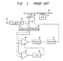
- a conventional servo system will be described hereinbelow with reference to Fig. 1.
- illustrated at numeral 50 is an optical disk equipped with pregroups and illustrated at numeral 52 is a light source such as a laser light source.
- the light beam emitted from the light source 52 passes through a collimator lens 53 so as to be converted into a parallel light beam, which is in turn reflected by means of a beam splitter 54 and then condensed onto the optical disk 50 through an objective lens 55.
- the reflected light beam from the optical disk 50 passes through the objective lens 55 and further through the beam splitter 54 so as to be directed to photodetectors 57 and 58.
- the outputs of the photodetectors 57 and 58 are respectively inputted to a gain-variable differential amplifier 59 the output of which is supplied to an equalizer 60 and further to a drive amplifier 61.
- the output of the drive amplifier 61 is led to a tracking drive apparatus 56, which in turn moves the objective lens 55 radially with respect to the optical disk 50 to perform the tracking servo operation.
- the tracking servo operation in the case of recording the information signal on the optical disk 50, the output power of the laser light source 52 is increased and the output light of the laser light source 52 is modulated in accordance with the information signal, thereby effecting the head recording on the optical disk 50.
- the gain of the tracking servo loop increases so as not to satisfy the optimal servo condition.
- the gain of the gain-variable differential amplifier 59 is required to be controlled by the output of an addition amplifier 63 so that the magnitude of the difference signal (a tracking signal) between the outputs of the photodetectors 57 and 58, i.e., the output of the gain-variable differential amplifier 59, becomes constant.
- the output of the gain-variable differential amplifier 59 takes a value to be obtained by dividing its input by the output of the addition ampliifer 63 (standardization).
- the magnitude of the tracking error signal is controllable to substantially become constant irrespective of the exchange of the optical disk 50.
- Numeral 64 is a filter for performing the AGC control (the control of the gain-variable differential amplifier 59) with an optimal frequency characteristic.
- the conventional tracking servo system is arranged such that the gain-variable differential amplifier is used in order to make constant the servo loop gain of the optical disk to optimize the operation of the servo loop
- the control precision of the AGC control can become insufficient when the gains and offsets of the addition amplifier 63 and gain-variable differential amplifier 59 vary because the AGC control loop cannot be constructed as a closed loop.
- the AGC control system is required to be also provided for the focusing servo system to thereby result in increase in the circuit amount and increase in the manufacturing cost.
- the digital processing means calculates an equation A ⁇ x/(B ⁇ y) to obtain the standardized servo error data.
- the digital processing means sets the attenuation factor of the attenuator means at the time of the inputting of the servo error signal with data obtained by multiplying z by the digital data after the analog-to-digital conversion of the sum signal whereby the digital data corresponding to the servo error signal is standardized with the digital data corresponding to said sum signal.
- a portion of a passage for inputting the servo error signal is arranged to be set to a predetermined electric potential at a predetermined time interval so that the set electric potential is registered as correction data to a register means, the digital processing means performing an offset correction with respect to the servo error signal and the sum signal on the basis of the registered correction data.
- the optical system is arranged to set its output to zero at a predetermined time so that the output of the photodetector means at the predetermined time is supplied as correction data to the analog-to-digital converter means so as to be registered to a register means, the digital processing means performing an offset correction with respect to the servo error signal and the sum signal on the basis of the registered correction data.
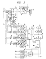
- a servo system according to an embodiment of the present invention.
- illustrated at numeral 1 is an optical disk
- illustrated at 2a is a fixed optical system for recording and reproducing an information signal from and on the optical disk 1
- illustrated at 2b is a movable optical system.
- the fixed optical system 2a is composed of a laser light source 3, a colimator lens 4, a beam splitter 5, half-mirrors 12a, 12b and photodetectors 13, 15, 16.
- the laser light source 3 emits a laser light beam which in turn passes through the collimator lens 4 so as to be converted into a parallel light beam.
- the parallel light beam from the collimator lens 4 passes through the beam splitter 5 before being outputted from the fixed optical system 2a toward the movable optical system 2b.
- the incident parallel light beam 6 from the fixed optical system 2a is first reflected by means of a mirror 7 to reach an objective lens 8 so as to be focused with respect to a recording layer of the optical disk 1.
- the parallel light beam 6 is arranged to have a diameter greater than the effective diameter of the objective lens 8.
- Illustrated at numeral 9 is a tracking actuator for moving the objective lens 8 with respect to the parallel light beam, i.e., moving the objective lens 8 radially with respect to the optical disk 1.
- Numeral 10 represents a focusing actuator for moving the objective lens 8 in directions perpendicular to the surfaces of the optical disk 1.
- the movable optical system 2b comprising the mirror 7, objective lens 8, tracking actuator 9 and focusing actuator 10 is arranged to be radially movable with respect to the optical disk 1 by means of a linear actuator 11.
- the linear actuator 11 is composed of a coil 11b and a magnetic circuit 11a.
- the light beam reflected on the optical disk 1 passes through the objective lens 8 so as to be again converted into a parallel reflection light beam which reaches a photodetector 13 through the mirror 7, beam splitter 5 and half-mirror 12a.
- the photodetector 13 is divided into two portions so as to output two electric signals in response to the reception of the parallel reflection light beam from the optical disk, the two electric signals being led to a differential amplifier 17 to take the difference between the two electric signals outputted from the two portions of the photodetector 13 to obtain a far-field tracking error signal.
- a lens which is positioned between the half-mirrors 12a and 12b and which is also responsive to the parallel reflection light beam from the optical disk 1 after being reflected by the beam splitter 5. After passing through the lens 14, the reflection light beam reaches the half-mirror 12b so as to be divided into two portions which in turn direct to second and third photodetectors 15 and 16.
- the lens 14 is arranged to cause the parallel reflection light beam to be focused at the intermediate position between the half-mirror 12 and the third photodetector 16. That is, the second and third photodetectors 15 and 16 receive the reflection light beams at positions before and after the local points.
- each of the second and third photodetectors 15 and 16 is divided into three photodetecting portions, and the photodetecting portions a and c of the second photodetector 15 are coupled to the photodetecting portion b of the third photodetector 16 and the photodetecting portions b of the second photodetector 15 is coupled to the photodetecting portions a and c of the third photodetector 16.
- the respective outputs of the second and third photodetectors 15 and 16 are coupled to a differential amplifier 19 so as to obtain a difference signal therebetween, i.e., a focusing error signal.
- Numeral 18 is an adder coupled to the first-mentioned tracking error signal detection photodetector 13 so as to obtain a tracking addition (or sum) signal corresponding to the light quantity incident on the first photodetector 13
- numeral 20 represents an adder coupled to the second and third photodetectors 15 and 16 so as to obtain a focusing addition signal corresponding to the light quantity incident on the second and third photodetectors 15 and 16. That is, the adder 18 outputs a signal indicative of the sum total output of the tracking error signal detector and the adder 20 outputs a signal indicative of the sum total output of the focusing error signal detector.
- the adder 18 outputs a signal indicative of the sum total output of the tracking error signal detector
- the adder 20 outputs a signal indicative of the sum total output of the focusing error signal detector.
- the differential amplifiers 17, 19 and adders 18, 20 are respectively coupled to attenuators 21 to 24 which are in turn coupled respectively to amplifiers 25 to 28.
- the attenuators 21 to 24 are also coupled respectively latch circuits 29 to 32 which are respectively coupled to a central processing unit (CPU) 38 to store data therefrom and set the attenuation amounts of the respective attenuators 21 to 24 in accordance with the stored data.
- the amplifiers 25 to 28 are respectively coupled to a multiplexer (MPX) 33 for selecting one of the outputs (33a to 33d) of the amplifiers 25 to 28 and outputting a signal indicative of the selected output to a sample-and-hold circuit (S/H) 34.
- MPX multiplexer
- the output of the sample-and-hold circuit 34 is supplied to an analog-to-digital converter (A/D) 35 so as to be converted into the corresponding digital signal.
- A/D analog-to-digital converter
- the output of the analog-to-digital converter 35 is supplied to a register 36 to be temporarily stored therein.
- Numeral 37 denotes a digital signal processor (DSP) which acts as a digital filter.
- DSP digital signal processor
- the DSP 37 is arranged such that the A/D-converted and standardized servo error signal is passed through an equalizer due to the digital filter so as to optimize the response of the servo system.
- the output signal of the DSP is supplied to a demultiplxer (DE-MPX) 39 so as to be converted into parallel signals which are in turn supplied as drive signals to actuator drivers 40 to 42 whose outputs are respectively supplied to the tracking actuator 9, focusing actuator 10 and linear actuator 11, thereby constituting the servo system.
- the CPU 38 supplies a portion of the data processed in the DSP 37 through an address data bus 38a to the above-mentioned latch circuits 29 to 32 so as to set the attenuation amounts of the attenuators 21 to 24.
- the CPU 38 generates an output b to the sample-and-hold circuit 34 in order to determine the sampling timing of the sample-and-hold circuit 34, and further generates an output c to the DSP 37 in order to determine the timing of the data exchange therebetween, and still further generates an output d to the MPX 33 for determining the switching timing of the MPX 33.
- the DE-MPX 39 is for again converting the data time-division-processed in the DSP 37 into parallel data.
- the DE-MPX 39 is equipped with a plurality of counters to count the time-divided serial data to produce a pulse train having pulse widths corresponding to the serial data, the PWM (pulse-width modulation) outputs being supplied to the actuator drivers 40 to 42 so as to control the drives of the tracking actuator 9, focusing actuator 10 and linear actuator 11.
- Numeral 43 represents a mode signal input terminal which is responsive to a mode signal for setting the servo system to the recording mode, reproducing mode or erasing mode.
- Fig. 3 is a timing chart when inputting the data through the register 36 to the DSP 37, the data being obtained with the input data selected by the MPX 33 being sampled and held by sample-and-hold circuit 34 and converted into a digital form by the A/D converter 35.
- references 2-1 to 2-4 represent the connection timings of the switch of the MPX 33.
- the reference 2-1 indicates that the input a of the MPX 33 is coupled to the output e of the MPX 33 when being in the high level state
- the reference 2-5 indicates a sample-and-hold pulse to be inputted to the sample-and-hold circuit 34.
- the voltage value held in response to the sample-and-hold pulse 2-5 is converted by the A/D converter 35 into a digital signal which is in turn read to the register 36 in response to the rising edge of a signal illustrated at reference 2-6 and then inputted to the DSP 37 in response to the falling edge of the 2-6 signal.
- the inputs a to d of the MPX 33 are supplied to the DSP 37 in the time-divided state.
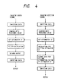
- Figs. 4 and 5 show the processing order of the signals inputted to the DSP 37.
- the input a (a tracking error signal) and input b (a tracking addition signal) of the MPX 33 are respectively inputted to the DSP 37 in the time-divided form so as to be processed in the order as illustrated by a flow chart of Fig. 4.
- the flow charts of Figs. 4 and 5 show the case that the servo system illustrated in Fig. 2 reaches the steady state, and the interval of the data reception may be set to about 10 ⁇ sec.
- the setting of the attenuation amount of the attenuator 21 is made through a calculation operation so that the tracking error signal a is divided by the tracking addition signal b (standardized).
- the divided data is filter-calculated and then outputted to the DE-MPX 39.
- the filter calculation corresponds to the equalizer function of the above-mentioned tracking servo system and is effected in order to optimize the response of the tracking servo system.
- the attenuators 21 and 22 are arranged so that the tracking error signal is divided by the tracking addition signal.
- the standard filter calculation is effected using the division result and the filter calculation result is outputted to the DE-MPX 39.
- the attenuation factors l/x and l/y are used so as to calculate A ⁇ x/(B ⁇ y), the calculation result being filter-calculated and then outputted to the DE-MPX 39.
- the attenuation factors of the attenuators to be used in the calculation are the values effective when passing through the attenuators.
- the calculation is effected by using the attenuation data of the attenuator set before the input of the data in consideration of the necessary time (delay time).
- the output of the laser light source 3 is modulated in accordance with the information signal to be recorded and further enhanced up to about 5 or 6 times the normal state.
- the light quantities to be incident on the photodetectors 13, 15 and 16 are also enlarged whereby the amplifiers 25 and 26 enter into the saturated states.
- the speed for changing the laser power from the reproducing state to the recording state is high (1 to 2 ⁇ sec)
- the time is required so that difficulty is encountered to normally operate the servo system.
- the CPU 38 is arranged to supply the attenuators 21 to 24 with data for changing the attenuation factors prior to the recording operation. After reaching the steady state, the operations as illustrated by the flow charts of Figs. 4 and 5 are executed, thereby improving the accuracy of the servo system.
- the differential amplifiers 17, 19 and the amplifiers 25 to 28 generally have the offset variations.
- the inputs of the differential amplifiers 17 and 18 are temporarily shorted at a predetermined time interval, and at that time the data (correction data) are independently inputted to the A/D converter 35 so as to be registered to the register 36 and the MPX 33 selects the outputs of the differential amplifiers 17, 18 and the amplifiers 25 to 28 so that, in terms of the servo error signal, the correction data inputted to the register 36 is subtracted from the data inputted to the A/D converter 35.
- the shorting arrangement is not illustrated, it is appropriate that, with analog switches or the like being inserted into the input stages of the differential amplifiers 17, 19 and/or the adders 18, 20, the CPU 38 gives a shorting command for an extremely short time below 100 ⁇ sec. This allows easily obtaining the correction data even if the system is in operation. Accordingly, it is possible to normally operate the system irrespective of the offset variations of the differential amplifiers and amplifiers. For obtaining the correction data, it is also appropriate to correct the offsets of the differential amplifier 17 and the amplifier 25 on the basis of the fact that, when the light beam formed by the objective lens 8 is at a mirror portion of the optical disk 1, the output of the differential amplifier 17 becomes zero.
- This correcting operation may be set to be completed with a short time below 100 ⁇ sec, whereby it is possible to easily obtain the correction data even if the system is in the operation such as reproducting operation.
- the attenuation factor of the attenuator is arranged to vary, so that the offset amount generated at the input side of the attenuator and the offset amount generated in the amplifier disposed at the output side thereof are separately detected so as to change the value of the correction data in accordance with the attenuation factor of the attenuator.
- the offset amount of the differential amplifier 17 is V1
- the attenuation factor of the attenuator 21 is G1
- the offset amount of the amplifier 25 is V2
- the output data X1 of the A/D converter 35 becomes as follows.
- the conventional system is arranged such that the AGC device is provided each channel for detecting the servo error signal of the optical disk, according to the present invention, all the processes can be effected only with one channel, that is, the batch process can be achieved.
- the attenuators 21 to 24 in accordance with the digital signal inputs, it is possible to easily suppress the DC drift and gain variation which are the problems inherent to the conventional analong type attenuator, thereby realizing the servo system with a high accuracy.
- the number of parts can be reduced and the adjusting time can considerably be reduced so as to realize the servo system with a low cost.
- the offset variations of the photodetectors, differential amplifiers, amplifiers and A/D converter can be corrected, thereby allowing the use of an element having a great offset variation.
- a digital servo system for use in an optical recording/reproducing apparatus equipped with an optical system for illuminating an optical recording medium with a light beam to record and reproduce an information signal on and from the optical recording medium, the servo system being for more accurately performing a tracking and focusing control of the light beam with respect to the optical recording medium.
- the servo system is provided with a plurality of photodetectors to obtain a servo error signal which is in turn supplied to an attenuator and then supplied to an analog-to-digital converter to be digitized so as to constitute a digital filter.
- the servo system is arranged so as to set the attenuation factor of the attenuator so that the input signal of the analog-to-digital converter is kept in a predetermined range. This permits the tracking and focusing control with a high precision and further allows an AGC amplifier having a high-speed automatic gain-controllable function to be arranged to be digitally controllable.
Abstract
Description
- The present invention relates generally to drives for optically recording and reproducing an information signal using an optical recording medium such as an optical disk, and more particularly to a servo system for use in such a optical recording/reproducing drive which is arranged so as to improve the focusing servo and the tracking servo to allow higher recording/reproducing accuracy.
- Generally, in recording/reproducing systems using an optical disk is known the so-called heat recording system where a laser beam spot having a diameter of about 1 µm is formed on a recording film provided on a track of an optical disk so as to allow physical variation of the recording film due to local temperature increase to record the information signal. One conventional servo system will be described hereinbelow with reference to Fig. 1. In Fig. 1, illustrated at
numeral 50 is an optical disk equipped with pregroups and illustrated atnumeral 52 is a light source such as a laser light source. The light beam emitted from thelight source 52 passes through acollimator lens 53 so as to be converted into a parallel light beam, which is in turn reflected by means of abeam splitter 54 and then condensed onto theoptical disk 50 through anobjective lens 55. On the other hand, the reflected light beam from theoptical disk 50 passes through theobjective lens 55 and further through thebeam splitter 54 so as to be directed tophotodetectors photodetectors differential amplifier 59 the output of which is supplied to anequalizer 60 and further to adrive amplifier 61. The output of thedrive amplifier 61 is led to atracking drive apparatus 56, which in turn moves theobjective lens 55 radially with respect to theoptical disk 50 to perform the tracking servo operation. In the tracking servo operation, in the case of recording the information signal on theoptical disk 50, the output power of thelaser light source 52 is increased and the output light of thelaser light source 52 is modulated in accordance with the information signal, thereby effecting the head recording on theoptical disk 50. At this time, since the power of the light incident on the trackingservo photodetectors differential amplifier 59 is required to be controlled by the output of anaddition amplifier 63 so that the magnitude of the difference signal (a tracking signal) between the outputs of thephotodetectors differential amplifier 59, becomes constant. As the result of the gain control, the output of the gain-variabledifferential amplifier 59 takes a value to be obtained by dividing its input by the output of the addition ampliifer 63 (standardization). Thus, the magnitude of the tracking error signal is controllable to substantially become constant irrespective of the exchange of theoptical disk 50. Numeral 64 is a filter for performing the AGC control (the control of the gain-variable differential amplifier 59) with an optimal frequency characteristic. - Although as described above the conventional tracking servo system is arranged such that the gain-variable differential amplifier is used in order to make constant the servo loop gain of the optical disk to optimize the operation of the servo loop, there is a problem which arises with such an arrangement, however, in that the control precision of the AGC control can become insufficient when the gains and offsets of the
addition amplifier 63 and gain-variabledifferential amplifier 59 vary because the AGC control loop cannot be constructed as a closed loop. In addition, the AGC control system is required to be also provided for the focusing servo system to thereby result in increase in the circuit amount and increase in the manufacturing cost. - It is therefore an object of the present invention to provide a servo system for an optical recording/reproducing drive which is capable of realizing a high control precision with a simple arrangement.
- A servo system for use in an optical recording/reproducing apparatus equipped with an optical system for illuminating an optical recording medium with a light beam to record and reproduce an information signal on and from the optical recording medium, the servo system being for performing a tracking and focusing control of the light beam with respect to the optical recording medium, comprising: photodetector means responsive to reflection light from the optical recording medium due to the light illumination of the optical system so as to output electric signals in correspondance with the incident light quantities; differential amplifier means responsive to the electric signals from the photodetector means so as to take the difference therebetween to output a servo error signal; adder means responsive to the electric signals from the photodetector means so as to take the sum of the electric signals to output a sum signal; attenuator means responsive to the servo error signal from the differential amplifier means and further responsive to the sum signal from the adder means so as to respectively attenuate the servo error signal and the sum signal with an attenuation factor which is changeable in accordance with a digital signal to be inputted; multiplexer means for successively selecting the outputs of the attenuator means; analog-to-digital converter means for successively converting the outputs of the multiplexer means into digital signals; and digital processing means responsive to digital data corresponding to the servo error signal and the sum signal from the analog-to-digital converter means, the digital processing means comparing the digital data with a predetermined value so as to output the digital signal to the attenuator means to set the attenuation factor of the attenuator means whereby the input signal of the analog-to-digital converter means is in a predetermined range and standardizing the digital data corresponding to said servo error signal with the digital data corresponding to the sum signal so as to perform a filter calculation with respect to the standardized servo error data to output a servo drive signal whereby the optical system is driven to effect the tracking and focusing control.
- Preferably, when the attenuation factor of the attenuator means at the inputting of the servo error signal is l/x, the digital data after the analog-to-digital conversion of the servo error signal is A, the attenuation factor of the attenuator at the time of the inputting of the sum signal is l/y and the digital data after the analog-to-digital conversion of the sum signal is B, the digital processing means calculates an equation A · x/(B · y) to obtain the standardized servo error data. When the attenuation factor of the attenuator means at the time of the inputting of the sum signal is l/z, the digital processing means sets the attenuation factor of the attenuator means at the time of the inputting of the servo error signal with data obtained by multiplying z by the digital data after the analog-to-digital conversion of the sum signal whereby the digital data corresponding to the servo error signal is standardized with the digital data corresponding to said sum signal.
- Further, preferably, a portion of a passage for inputting the servo error signal is arranged to be set to a predetermined electric potential at a predetermined time interval so that the set electric potential is registered as correction data to a register means, the digital processing means performing an offset correction with respect to the servo error signal and the sum signal on the basis of the registered correction data. The optical system is arranged to set its output to zero at a predetermined time so that the output of the photodetector means at the predetermined time is supplied as correction data to the analog-to-digital converter means so as to be registered to a register means, the digital processing means performing an offset correction with respect to the servo error signal and the sum signal on the basis of the registered correction data.
- The object and features of the present invention will become more readily apparent from the following detailed description of the preferred embodiment taken in conjunction with the accompanying drawings in which:
- Fig. 1 is a block diagram showing an arrangement of a conventional tracking servo system;
- Fig. 2 is a block diagram showing an arrangement of a servo system according to an embodiment of the present invention;
- Fig. 3 is a timing chart for describing the operation timing of the Fig. 2 servo system; and
- Figs. 4 and 5 are flow charms for describing the operation of the Fig. 2 servo system.
- Referring now to Fig. 2, there is illustrated a servo system according to an embodiment of the present invention. In Fig. 2, illustrated at
numeral 1 is an optical disk, illustrated at 2a is a fixed optical system for recording and reproducing an information signal from and on theoptical disk 1 and illustrated at 2b is a movable optical system. The fixedoptical system 2a is composed of alaser light source 3, acolimator lens 4, abeam splitter 5, half-mirrors photodetectors laser light source 3 emits a laser light beam which in turn passes through thecollimator lens 4 so as to be converted into a parallel light beam. The parallel light beam from thecollimator lens 4 passes through thebeam splitter 5 before being outputted from the fixedoptical system 2a toward the movableoptical system 2b. In the movableoptical system 2b, the incidentparallel light beam 6 from the fixedoptical system 2a is first reflected by means of amirror 7 to reach anobjective lens 8 so as to be focused with respect to a recording layer of theoptical disk 1. Here, theparallel light beam 6 is arranged to have a diameter greater than the effective diameter of theobjective lens 8. Illustrated atnumeral 9 is a tracking actuator for moving theobjective lens 8 with respect to the parallel light beam, i.e., moving theobjective lens 8 radially with respect to theoptical disk 1.Numeral 10 represents a focusing actuator for moving theobjective lens 8 in directions perpendicular to the surfaces of theoptical disk 1. The movableoptical system 2b comprising themirror 7,objective lens 8, trackingactuator 9 and focusingactuator 10 is arranged to be radially movable with respect to theoptical disk 1 by means of alinear actuator 11. Thelinear actuator 11 is composed of acoil 11b and amagnetic circuit 11a. - On the other hand, the light beam reflected on the
optical disk 1 passes through theobjective lens 8 so as to be again converted into a parallel reflection light beam which reaches aphotodetector 13 through themirror 7,beam splitter 5 and half-mirror 12a. Thephotodetector 13 is divided into two portions so as to output two electric signals in response to the reception of the parallel reflection light beam from the optical disk, the two electric signals being led to adifferential amplifier 17 to take the difference between the two electric signals outputted from the two portions of thephotodetector 13 to obtain a far-field tracking error signal. Further, illustrated at 14 is a lens which is positioned between the half-mirrors optical disk 1 after being reflected by thebeam splitter 5. After passing through thelens 14, the reflection light beam reaches the half-mirror 12b so as to be divided into two portions which in turn direct to second andthird photodetectors lens 14 is arranged to cause the parallel reflection light beam to be focused at the intermediate position between the half-mirror 12 and thethird photodetector 16. That is, the second andthird photodetectors actuator 9 is controlled so that the diameters of the divided reflection light beams become constant, thereby performing the focusing control. Each of the second andthird photodetectors second photodetector 15 are coupled to the photodetecting portion b of thethird photodetector 16 and the photodetecting portions b of thesecond photodetector 15 is coupled to the photodetecting portions a and c of thethird photodetector 16. The respective outputs of the second andthird photodetectors differential amplifier 19 so as to obtain a difference signal therebetween, i.e., a focusing error signal.Numeral 18 is an adder coupled to the first-mentioned tracking errorsignal detection photodetector 13 so as to obtain a tracking addition (or sum) signal corresponding to the light quantity incident on thefirst photodetector 13, andnumeral 20 represents an adder coupled to the second andthird photodetectors third photodetectors adder 18 outputs a signal indicative of the sum total output of the tracking error signal detector and theadder 20 outputs a signal indicative of the sum total output of the focusing error signal detector. Thus, it is possible to simultaneously obtain the servo error signals and the signals representative of the sum totals of the photodetector outputs. - As illustrated in Fig. 2, the
differential amplifiers adders attenuators 21 to 24 which are in turn coupled respectively to amplifiers 25 to 28. Theattenuators 21 to 24 are also coupled respectivelylatch circuits 29 to 32 which are respectively coupled to a central processing unit (CPU) 38 to store data therefrom and set the attenuation amounts of therespective attenuators 21 to 24 in accordance with the stored data. Theamplifiers 25 to 28 are respectively coupled to a multiplexer (MPX) 33 for selecting one of the outputs (33a to 33d) of theamplifiers 25 to 28 and outputting a signal indicative of the selected output to a sample-and-hold circuit (S/H) 34. The output of the sample-and-hold circuit 34 is supplied to an analog-to-digital converter (A/D) 35 so as to be converted into the corresponding digital signal. The output of the analog-to-digital converter 35 is supplied to aregister 36 to be temporarily stored therein. Numeral 37 denotes a digital signal processor (DSP) which acts as a digital filter. Here, the TMS320C25 manufactured by TI Co., Ltd can be used as thedigital signal processor 37, for instance. The DSP 37 is arranged such that the A/D-converted and standardized servo error signal is passed through an equalizer due to the digital filter so as to optimize the response of the servo system. The output signal of the DSP is supplied to a demultiplxer (DE-MPX) 39 so as to be converted into parallel signals which are in turn supplied as drive signals toactuator drivers 40 to 42 whose outputs are respectively supplied to thetracking actuator 9, focusingactuator 10 andlinear actuator 11, thereby constituting the servo system. The CPU 38 supplies a portion of the data processed in theDSP 37 through anaddress data bus 38a to the above-mentionedlatch circuits 29 to 32 so as to set the attenuation amounts of theattenuators 21 to 24. In addition, the CPU 38 generates an output b to the sample-and-hold circuit 34 in order to determine the sampling timing of the sample-and-hold circuit 34, and further generates an output c to theDSP 37 in order to determine the timing of the data exchange therebetween, and still further generates an output d to theMPX 33 for determining the switching timing of theMPX 33. The DE-MPX 39 is for again converting the data time-division-processed in theDSP 37 into parallel data. For instance, the DE-MPX 39 is equipped with a plurality of counters to count the time-divided serial data to produce a pulse train having pulse widths corresponding to the serial data, the PWM (pulse-width modulation) outputs being supplied to theactuator drivers 40 to 42 so as to control the drives of the trackingactuator 9, focusingactuator 10 andlinear actuator 11. Numeral 43 represents a mode signal input terminal which is responsive to a mode signal for setting the servo system to the recording mode, reproducing mode or erasing mode. - A description will be made hereinbelow with reference to Figs. 3 to 5 in terms of the operation of the above-described servo system. Fig. 3 is a timing chart when inputting the data through the
register 36 to theDSP 37, the data being obtained with the input data selected by theMPX 33 being sampled and held by sample-and-hold circuit 34 and converted into a digital form by the A/D converter 35. In Fig. 3, references 2-1 to 2-4 represent the connection timings of the switch of theMPX 33. For example, the reference 2-1 indicates that the input a of theMPX 33 is coupled to the output e of theMPX 33 when being in the high level state, and the reference 2-5 indicates a sample-and-hold pulse to be inputted to the sample-and-hold circuit 34. The voltage value held in response to the sample-and-hold pulse 2-5 is converted by the A/D converter 35 into a digital signal which is in turn read to theregister 36 in response to the rising edge of a signal illustrated at reference 2-6 and then inputted to theDSP 37 in response to the falling edge of the 2-6 signal. As obvious from above, the inputs a to d of theMPX 33 are supplied to theDSP 37 in the time-divided state. - Secondly, a description will be made hereinbelow with reference to Figs. 4 and 5 in terms of the processing order of the signals inputted to the
DSP 37. The input a (a tracking error signal) and input b (a tracking addition signal) of theMPX 33 are respectively inputted to theDSP 37 in the time-divided form so as to be processed in the order as illustrated by a flow chart of Fig. 4. Here, the flow charts of Figs. 4 and 5 show the case that the servo system illustrated in Fig. 2 reaches the steady state, and the interval of the data reception may be set to about 10 µsec. In the flow chart of Fig. 4, the setting of the attenuation amount of theattenuator 21 is made through a calculation operation so that the tracking error signal a is divided by the tracking addition signal b (standardized). The divided data is filter-calculated and then outputted to theDE-MPX 39. The filter calculation corresponds to the equalizer function of the above-mentioned tracking servo system and is effected in order to optimize the response of the tracking servo system. On the other hand, in the flow chart of Fig. 5, under the condition that theamplifiers attenuators DE-MPX 39. In this case, in order to correct the portions of the inputted data A and B attenuated in the corresponding attenuators, the attenuation factors l/x and l/y are used so as to calculate A·x/(B·y), the calculation result being filter-calculated and then outputted to theDE-MPX 39. The attenuation factors of the attenuators to be used in the calculation are the values effective when passing through the attenuators. Thus, in the case that a time (for example, 10 µsec) is necessary until the attenuator operates in accordance with the set value, after the attenuation factor setting data are inputted through thelatch circuits attenuators - In the flow charts of Figs. 4 and 5, all the data inputted are always compared with a reference value so as to prevent the deviation from the operation ranges of the
amplifiers D converter 35 has an 8-bit structure, the reference value may be set to ± 70% with respect to the central value. Here, the flow charts of Figs. 4 and 5 respectively advance in the time-division state, while the flow chart for procesing the servo error signal may be executed with less delay time and the other flow chart may be executed so as to ensure the operation of the minimum condition. Accordingly, in the execution of the flow chart, the operation time (for example, between the input of data and the comparison with the reference value) is not constant. Although the above description has been made in terms of the tracking servo system, it is also possible to perform the above-described operation for the focusing servo system. Further, a description of the loop for controlling thelinear actuator 11 is omitted. - In the case that the Fig. 2 recording/reproducing drive receives the recording command through the mode signal input terminal 43 when being in the reproducing state, the output of the
laser light source 3 is modulated in accordance with the information signal to be recorded and further enhanced up to about 5 or 6 times the normal state. At this time, the light quantities to be incident on thephotodetectors amplifiers DSP 37 to theattenuators 21 to 24, the time is required so that difficulty is encountered to normally operate the servo system. For this case, the CPU 38 is arranged to supply theattenuators 21 to 24 with data for changing the attenuation factors prior to the recording operation. After reaching the steady state, the operations as illustrated by the flow charts of Figs. 4 and 5 are executed, thereby improving the accuracy of the servo system. - The
differential amplifiers amplifiers 25 to 28 generally have the offset variations. Thus, in this invention, the inputs of thedifferential amplifiers D converter 35 so as to be registered to theregister 36 and theMPX 33 selects the outputs of thedifferential amplifiers amplifiers 25 to 28 so that, in terms of the servo error signal, the correction data inputted to theregister 36 is subtracted from the data inputted to the A/D converter 35. Although the shorting arrangement is not illustrated, it is appropriate that, with analog switches or the like being inserted into the input stages of thedifferential amplifiers adders differential amplifier 17 and theamplifier 25 on the basis of the fact that, when the light beam formed by theobjective lens 8 is at a mirror portion of theoptical disk 1, the output of thedifferential amplifier 17 becomes zero. Moreover, it is also appropriate to correct the drifts of the photodetectors, differential amplifiers, amplifiers and A/D converter on the basis of the fact that, when the output of thelaser light source 3 is temporarily set to zero, all the outputs of the photodetectors become zero. This correcting operation may be set to be completed with a short time below 100 µsec, whereby it is possible to easily obtain the correction data even if the system is in the operation such as reproducting operation. - Here, in the case of performing the offset correction, the attenuation factor of the attenuator is arranged to vary, so that the offset amount generated at the input side of the attenuator and the offset amount generated in the amplifier disposed at the output side thereof are separately detected so as to change the value of the correction data in accordance with the attenuation factor of the attenuator. For instance, in Fig. 2, in the case that the input of the
differential amplifier 17 is shorted, when the offset amount of thedifferential amplifier 17 is V1, the attenuation factor of theattenuator 21 is G1 and the offset amount of theamplifier 25 is V2, the output data X1 of the A/D converter 35 becomes as follows.

When the attenuation factor of theattenuator 21 is changed from G1 to G2, the output data X2 of the A/D converter 35 becomes as follows.

From the aforementioned two equations, the offset amounts V1 and V2 are obtained. In terms of the offset amount V1, the correction data for the offset to be corrected by the attenuation factor of theattenuator 21 is changed so as to perform the correction of the output of the A/D converter 35. On the other hand, in terms of the offset amount V2, the correction is effected irrespective of the attenuation factor of the attenuator. Thus, it is possible to always obtain the correction data even if the attenuation factor of the attenuator varies. - As described above, although the conventional system is arranged such that the AGC device is provided each channel for detecting the servo error signal of the optical disk, according to the present invention, all the processes can be effected only with one channel, that is, the batch process can be achieved. Further, because of being arranged to control the
attenuators 21 to 24 in accordance with the digital signal inputs, it is possible to easily suppress the DC drift and gain variation which are the problems inherent to the conventional analong type attenuator, thereby realizing the servo system with a high accuracy. In addition, the number of parts can be reduced and the adjusting time can considerably be reduced so as to realize the servo system with a low cost. Moreover, since the offset variations of the photodetectors, differential amplifiers, amplifiers and A/D converter can be corrected, thereby allowing the use of an element having a great offset variation. - It should be understood that the foregoing relates to only a preferred embodiment of the present invention, and that it is intended to cover all changes and modifications of the embodiment of the invention herein used for the purposes of the disclosure, which do not constitute departures from the spirit and scope of the invention.
- A digital servo system for use in an optical recording/reproducing apparatus equipped with an optical system for illuminating an optical recording medium with a light beam to record and reproduce an information signal on and from the optical recording medium, the servo system being for more accurately performing a tracking and focusing control of the light beam with respect to the optical recording medium. The servo system is provided with a plurality of photodetectors to obtain a servo error signal which is in turn supplied to an attenuator and then supplied to an analog-to-digital converter to be digitized so as to constitute a digital filter. The servo system is arranged so as to set the attenuation factor of the attenuator so that the input signal of the analog-to-digital converter is kept in a predetermined range. This permits the tracking and focusing control with a high precision and further allows an AGC amplifier having a high-speed automatic gain-controllable function to be arranged to be digitally controllable.
Claims (5)
- A servo system for use in an optical recording/reproducing apparatus equipped with an optical system for illuminating an optical recording medium with a light beam to record and reproduce an information signal on and from said optical recording medium, said servo system being for performing a tracking and focusing control of the light beam with respect to said optical recording medium, comprising:
photodetector means responsive to reflection light from said optical recording medium due to the light illumination of said optical system so as to output electric signals in correspondance with the incident light quantities;
differential amplifier means responsive to the electric signals from said photodetector means so as to take the difference therebetween to output a servo error signal;
adder means responsive to the electric signals from said photodetector means so as to take the sum of the electric signals to output a sum signal;
attenuator means responsive to said servo error signal from said differential amplifier means and further responsive to said sum signal from said adder means so as to respectively attenuate said servo error signal and said sum signal with an attenuation factor which is changeable in accordance with a digital signal to be inputted;
multiplexer means for successively selecting the outputs of said attenuator means;
analog-to-digital converter means for successively converting the outputs of said multiplexer means into digital signals; and
digital processing means responsive to digital data corresponding to said servo error signal and said sum signal from said analog-to-digital converter means, said digital processing means comparing said digital data with a predetermined value so as to output said digital signal to said attenuator means to set the attenuation factor of said attenuator means whereby the input signal of said analog-to-digital converter means is in a predetermined range and standardizing said digital data corresponding to said servo error signal with said digital data corresponding to said sum signal so as to perform a filter calculation with respect to the standardized servo error data to output a servo drive signal whereby said optical system is driven to effect the tracking and focusing control. - A servo system as claimed in claim 1, wherein, when the attenuation factor of said attenuator means at the inputting of said servo error signal is l/x, the digital data after the analog-to-digital conversion of said servo error signal is A, the attenuation factor of said attenuator at the time of the inputting of said sum signal is l/y and the digital data after the analog-to-digital conversion of said sum signal is B, said digital processing means calculates an equation A · x/(B · y) to obtain the standardized servo error data.
- A servo system as claimed in claim 1, wherein, when the attenuation factor of said attenuator means at the time of the inputting of said sum signal is l/z, said digital processing means sets the attenuation factor of said attenuator means at the time of the inputting of said servo error signal with data obtained by multiplying z by the digital data after the analog-to-digital conversion of said sum signal whereby the digital data corresponding to said servo error signal is standardized with the digital data corresponding to said sum signal.
- A servo system as claimed in claim 1, further comprising register means, and wherein a portion of a passage for inputting said servo error signal is arranged to be set to a predetermined electric potential at a predetermined time interval so that the set electric potential is registered as correction data to said register means, said digital processing means performing an offset correction with respect to said servo error signal and said sum signal on the basis of the registered correction data.
- A servo system as claimed in claim 1, further comprising register means, and wherein said optical system is arranged to set its output to zero at a predetermined time so that the output of said photodetector means at the predetermined time is supplied as correction data to said analog-to-digital converter means so as to be registered to said register means, said digital processing means performing an offset correction with respect to said servo error signal and said sum signal on the basis of the registered correction data.
Applications Claiming Priority (2)
| Application Number | Priority Date | Filing Date | Title |
|---|---|---|---|
| JP131561/90 | 1990-05-22 | ||
| JP2131561A JP2540224B2 (en) | 1990-05-22 | 1990-05-22 | Optical disk servo device |
Publications (3)
| Publication Number | Publication Date |
|---|---|
| EP0458319A2 true EP0458319A2 (en) | 1991-11-27 |
| EP0458319A3 EP0458319A3 (en) | 1992-08-12 |
| EP0458319B1 EP0458319B1 (en) | 1997-04-09 |
Family
ID=15060946
Family Applications (1)
| Application Number | Title | Priority Date | Filing Date |
|---|---|---|---|
| EP91108326A Expired - Lifetime EP0458319B1 (en) | 1990-05-22 | 1991-05-22 | Servo system for optical recording reproducing drive |
Country Status (4)
| Country | Link |
|---|---|
| US (1) | US5155716A (en) |
| EP (1) | EP0458319B1 (en) |
| JP (1) | JP2540224B2 (en) |
| DE (1) | DE69125524T2 (en) |
Cited By (4)
| Publication number | Priority date | Publication date | Assignee | Title |
|---|---|---|---|---|
| EP0649134A1 (en) * | 1993-10-13 | 1995-04-19 | Canon Kabushiki Kaisha | Magnetooptical disc apparatus having single micro-processor |
| EP0829861A2 (en) * | 1995-01-25 | 1998-03-18 | Discovision Associates | Servo control system for information storage device |
| WO1998049679A2 (en) * | 1997-04-25 | 1998-11-05 | Koninklijke Philips Electronics N.V. | Apparatus and detection unit for scanning an optically readable record carrier |
| WO2005050629A2 (en) * | 2003-10-30 | 2005-06-02 | Thomson Licensing | Differential phase detector |
Families Citing this family (15)
| Publication number | Priority date | Publication date | Assignee | Title |
|---|---|---|---|---|
| US5677899A (en) | 1991-02-15 | 1997-10-14 | Discovision Associates | Method for moving carriage assembly from initial position to target position relative to storage medium |
| JPH06111345A (en) * | 1992-09-29 | 1994-04-22 | Matsushita Electric Ind Co Ltd | Optical head controller |
| US5495466A (en) * | 1994-01-10 | 1996-02-27 | Eastman Kodak Company | Write verification in an optical recording system by sensing mark formation while writing |
| US6434087B1 (en) | 1995-01-25 | 2002-08-13 | Discovision Associates | Optical disc system and method for controlling bias coil and light source to process information on a storage medium |
| JPH09151786A (en) * | 1995-11-30 | 1997-06-10 | Aisin Seiki Co Ltd | Manufacture of piston for internal combustion engine |
| TW464849B (en) * | 1999-03-31 | 2001-11-21 | Matsushita Electric Ind Co Ltd | Optical disc controller and optical disc device |
| US6519213B1 (en) * | 1999-06-29 | 2003-02-11 | Oak Technology, Inc. | Method and apparatus for reading data from a disk |
| US7522480B2 (en) | 2001-01-25 | 2009-04-21 | Dphi Acquisitions, Inc. | Digital tracking servo system with multi-track seek with an acceleration clamp |
| US6809995B2 (en) * | 2001-01-25 | 2004-10-26 | Dphi Acquisitions, Inc. | Digital focus and tracking servo system |
| US7023766B2 (en) * | 2001-01-25 | 2006-04-04 | Dphi Acquisitions, Inc. | Flexible servicing of servo algorithms using a digital signal processor |
| TWI248610B (en) * | 2003-04-07 | 2006-02-01 | Mediatek Inc | Method and related apparatus for deriving a tracking error signal |
| JP4492810B2 (en) * | 2006-02-14 | 2010-06-30 | ソニー株式会社 | Attenuation adjustment circuit, optical disc drive apparatus, attenuation adjustment method, and address information acquisition method |
| US7706219B2 (en) * | 2006-06-05 | 2010-04-27 | Mediatek Inc. | Signal processing apparatus and method for an optical disc drive |
| JP2008276869A (en) * | 2007-04-27 | 2008-11-13 | Victor Co Of Japan Ltd | Optical pickup drive method and optical disk device |
| US20130105708A1 (en) * | 2011-11-02 | 2013-05-02 | Gordon Bennett | Narrow band fluorophore exciter |
Citations (4)
| Publication number | Priority date | Publication date | Assignee | Title |
|---|---|---|---|---|
| JPS60138740A (en) * | 1983-12-27 | 1985-07-23 | Sony Corp | Tracking servo circuit of optical disc player |
| JPS60187940A (en) * | 1984-03-07 | 1985-09-25 | Hitachi Ltd | Optical recording and reproducing device |
| JPS63204519A (en) * | 1987-02-20 | 1988-08-24 | Matsushita Commun Ind Co Ltd | Servo circuit for perforating type additional optical disk |
| EP0304932A2 (en) * | 1987-08-28 | 1989-03-01 | Fujitsu Limited | Optical disk access system |
Family Cites Families (5)
| Publication number | Priority date | Publication date | Assignee | Title |
|---|---|---|---|---|
| US4485414A (en) * | 1980-07-07 | 1984-11-27 | Ampex Corporation | Servo system for positioning a movable transducing head assembly |
| JP2565485B2 (en) * | 1984-09-14 | 1996-12-18 | オリンパス光学工業株式会社 | Optical recording / reproducing device |
| JPH06101127B2 (en) * | 1985-03-13 | 1994-12-12 | シャープ株式会社 | Optical head |
| JPH0758555B2 (en) * | 1986-11-07 | 1995-06-21 | ロ−ム株式会社 | Servo device for disk playback equipment |
| JP2703226B2 (en) * | 1987-03-31 | 1998-01-26 | 株式会社東芝 | Tracking servo circuit |
-
1990
- 1990-05-22 JP JP2131561A patent/JP2540224B2/en not_active Expired - Fee Related
-
1991
- 1991-05-21 US US07/703,639 patent/US5155716A/en not_active Expired - Lifetime
- 1991-05-22 EP EP91108326A patent/EP0458319B1/en not_active Expired - Lifetime
- 1991-05-22 DE DE69125524T patent/DE69125524T2/en not_active Expired - Lifetime
Patent Citations (4)
| Publication number | Priority date | Publication date | Assignee | Title |
|---|---|---|---|---|
| JPS60138740A (en) * | 1983-12-27 | 1985-07-23 | Sony Corp | Tracking servo circuit of optical disc player |
| JPS60187940A (en) * | 1984-03-07 | 1985-09-25 | Hitachi Ltd | Optical recording and reproducing device |
| JPS63204519A (en) * | 1987-02-20 | 1988-08-24 | Matsushita Commun Ind Co Ltd | Servo circuit for perforating type additional optical disk |
| EP0304932A2 (en) * | 1987-08-28 | 1989-03-01 | Fujitsu Limited | Optical disk access system |
Non-Patent Citations (3)
| Title |
|---|
| PATENT ABSTRACTS OF JAPAN vol. 10, no. 41 (P-429)(2098) 18 February 1986 & JP-A-60 187 940 ( HITACHI SEISAKUSHO K.K. ) 25 September 1985 * |
| PATENT ABSTRACTS OF JAPAN vol. 12, no. 494 (P-805)23 December 1988 & JP-A-63 204 519 ( MATSUSHITA COMMUN IND CO LTD ) 24 August 1988 * |
| PATENT ABSTRACTS OF JAPAN vol. 9, no. 308 (P-410)(2031) 4 December 1985 & JP-A-60 138 740 ( SONY K.K. ) 23 July 1985 * |
Cited By (11)
| Publication number | Priority date | Publication date | Assignee | Title |
|---|---|---|---|---|
| EP0649134A1 (en) * | 1993-10-13 | 1995-04-19 | Canon Kabushiki Kaisha | Magnetooptical disc apparatus having single micro-processor |
| US5699330A (en) * | 1993-10-13 | 1997-12-16 | Canon Kabushiki Kaisha | Magnetooptical disc apparatus having single micro-processor for controlling input/output processing of information by causing an interruption in the processing |
| EP0829861A2 (en) * | 1995-01-25 | 1998-03-18 | Discovision Associates | Servo control system for information storage device |
| EP0838811A2 (en) * | 1995-01-25 | 1998-04-29 | Discovision Associates | Analog to digital converter and assembly to normalize servo error signals and multiplex reference voltage inputs and digital outputs and optical drive system including same |
| EP0838811A3 (en) * | 1995-01-25 | 1999-04-14 | Discovision Associates | Analog to digital converter and assembly to normalize servo error signals and multiplex reference voltage inputs and digital outputs and optical drive system including same |
| EP0829861A3 (en) * | 1995-01-25 | 1999-04-14 | Discovision Associates | Servo control system for information storage device |
| WO1998049679A2 (en) * | 1997-04-25 | 1998-11-05 | Koninklijke Philips Electronics N.V. | Apparatus and detection unit for scanning an optically readable record carrier |
| WO1998049679A3 (en) * | 1997-04-25 | 1999-02-04 | Koninkl Philips Electronics Nv | Apparatus and detection unit for scanning an optically readable record carrier |
| US6137755A (en) * | 1997-04-25 | 2000-10-24 | U.S. Philips Corporation | Deriving a tracking error signal from a time difference between detector signals |
| WO2005050629A2 (en) * | 2003-10-30 | 2005-06-02 | Thomson Licensing | Differential phase detector |
| WO2005050629A3 (en) * | 2003-10-30 | 2005-07-21 | Thomson Licensing Sa | Differential phase detector |
Also Published As
| Publication number | Publication date |
|---|---|
| DE69125524D1 (en) | 1997-05-15 |
| EP0458319A3 (en) | 1992-08-12 |
| US5155716A (en) | 1992-10-13 |
| JP2540224B2 (en) | 1996-10-02 |
| JPH0426930A (en) | 1992-01-30 |
| EP0458319B1 (en) | 1997-04-09 |
| DE69125524T2 (en) | 1997-11-13 |
Similar Documents
| Publication | Publication Date | Title |
|---|---|---|
| EP0458319B1 (en) | Servo system for optical recording reproducing drive | |
| KR910006081B1 (en) | Optical disk player | |
| US4835752A (en) | Device for driving and controlling optical head for use in optical disk system | |
| JPH0845090A (en) | Method and apparatus for control of focus | |
| US5077716A (en) | Optical recording and reproducing system having an accurate high-speed optical head positioning apparatus | |
| US4661942A (en) | Control apparatus for information storage and retrieval system | |
| EP0731455A2 (en) | Optical information recording and reproducing apparatus and method | |
| US5862111A (en) | Optical disk device which performs auto gain control process on servo signals which perform illuminating control of a light beam on the disk's recording surface | |
| US5050149A (en) | Servo device for disc player | |
| US5291466A (en) | Automatic control system for a tracking servo unbalance of optical disk player | |
| EP0497548B1 (en) | Apparatus for detecting position of light spot | |
| KR100411218B1 (en) | Optical reproduction apparatus | |
| EP0654785B1 (en) | Error correcting apparatus with error correcting signal holding function | |
| KR100189911B1 (en) | Apparatus for optical disc drive servo and the method thereof | |
| US4794244A (en) | Method and apparatus for detecting focussing position deviation of read/write apparatus in an optical recording medium | |
| US4992652A (en) | Focus error detecting circuit for disk player | |
| US6016294A (en) | AGC circuit with a digital divider for an optical disc drive unit | |
| US4926407A (en) | Optical data processor | |
| KR19990011987A (en) | Tracking Servo Device of DVD System | |
| US5402404A (en) | Optical disc apparatus having automatic gain control circuit of open loop type | |
| US5659527A (en) | Optical disk drive with use of sampled preceding focus or tracking error signal in response to detection of spiked noise or offset | |
| JP3257655B2 (en) | Optical information recording / reproducing device | |
| JP2778365B2 (en) | Track access control device and tracking control device for optical disk device | |
| JP2692060B2 (en) | Recording and playback device | |
| JPH01194143A (en) | Positioner device |
Legal Events
| Date | Code | Title | Description |
|---|---|---|---|
| PUAI | Public reference made under article 153(3) epc to a published international application that has entered the european phase |
Free format text: ORIGINAL CODE: 0009012 |
|
| 17P | Request for examination filed |
Effective date: 19910621 |
|
| AK | Designated contracting states |
Kind code of ref document: A2 Designated state(s): DE FR GB |
|
| PUAL | Search report despatched |
Free format text: ORIGINAL CODE: 0009013 |
|
| AK | Designated contracting states |
Kind code of ref document: A3 Designated state(s): DE FR GB |
|
| 17Q | First examination report despatched |
Effective date: 19940811 |
|
| GRAG | Despatch of communication of intention to grant |
Free format text: ORIGINAL CODE: EPIDOS AGRA |
|
| GRAH | Despatch of communication of intention to grant a patent |
Free format text: ORIGINAL CODE: EPIDOS IGRA |
|
| GRAH | Despatch of communication of intention to grant a patent |
Free format text: ORIGINAL CODE: EPIDOS IGRA |
|
| GRAA | (expected) grant |
Free format text: ORIGINAL CODE: 0009210 |
|
| AK | Designated contracting states |
Kind code of ref document: B1 Designated state(s): DE FR GB |
|
| ET | Fr: translation filed | ||
| REF | Corresponds to: |
Ref document number: 69125524 Country of ref document: DE Date of ref document: 19970515 |
|
| PLBE | No opposition filed within time limit |
Free format text: ORIGINAL CODE: 0009261 |
|
| STAA | Information on the status of an ep patent application or granted ep patent |
Free format text: STATUS: NO OPPOSITION FILED WITHIN TIME LIMIT |
|
| 26N | No opposition filed | ||
| REG | Reference to a national code |
Ref country code: GB Ref legal event code: IF02 |
|
| REG | Reference to a national code |
Ref country code: GB Ref legal event code: 746 Effective date: 20100127 |
|
| PGFP | Annual fee paid to national office [announced via postgrant information from national office to epo] |
Ref country code: GB Payment date: 20100329 Year of fee payment: 20 |
|
| PGFP | Annual fee paid to national office [announced via postgrant information from national office to epo] |
Ref country code: FR Payment date: 20100525 Year of fee payment: 20 |
|
| PGFP | Annual fee paid to national office [announced via postgrant information from national office to epo] |
Ref country code: DE Payment date: 20100519 Year of fee payment: 20 |
|
| REG | Reference to a national code |
Ref country code: DE Ref legal event code: R071 Ref document number: 69125524 Country of ref document: DE |
|
| REG | Reference to a national code |
Ref country code: GB Ref legal event code: PE20 Expiry date: 20110521 |
|
| PG25 | Lapsed in a contracting state [announced via postgrant information from national office to epo] |
Ref country code: GB Free format text: LAPSE BECAUSE OF EXPIRATION OF PROTECTION Effective date: 20110521 |
|
| PG25 | Lapsed in a contracting state [announced via postgrant information from national office to epo] |
Ref country code: DE Free format text: LAPSE BECAUSE OF EXPIRATION OF PROTECTION Effective date: 20110523 |