EP0458092A2 - Curved array ultrasonic transducer assembly and its method of manufacture - Google Patents
Curved array ultrasonic transducer assembly and its method of manufacture Download PDFInfo
- Publication number
- EP0458092A2 EP0458092A2 EP91106978A EP91106978A EP0458092A2 EP 0458092 A2 EP0458092 A2 EP 0458092A2 EP 91106978 A EP91106978 A EP 91106978A EP 91106978 A EP91106978 A EP 91106978A EP 0458092 A2 EP0458092 A2 EP 0458092A2
- Authority
- EP
- European Patent Office
- Prior art keywords
- circuit board
- transducer
- array
- flexible circuit
- traces
- Prior art date
- Legal status (The legal status is an assumption and is not a legal conclusion. Google has not performed a legal analysis and makes no representation as to the accuracy of the status listed.)
- Withdrawn
Links
- 238000000034 method Methods 0.000 title claims description 13
- 238000004519 manufacturing process Methods 0.000 title claims description 5
- 239000000463 material Substances 0.000 claims description 8
- 239000000919 ceramic Substances 0.000 claims description 5
- 239000004020 conductor Substances 0.000 claims description 3
- 238000005452 bending Methods 0.000 claims 3
- 239000011810 insulating material Substances 0.000 claims 1
- 238000003491 array Methods 0.000 description 3
- 239000002305 electric material Substances 0.000 description 3
- 238000003384 imaging method Methods 0.000 description 2
- 239000012212 insulator Substances 0.000 description 2
- 238000005476 soldering Methods 0.000 description 2
- 210000001835 viscera Anatomy 0.000 description 2
- 239000002390 adhesive tape Substances 0.000 description 1
- 230000004075 alteration Effects 0.000 description 1
- 230000000712 assembly Effects 0.000 description 1
- 238000000429 assembly Methods 0.000 description 1
- 210000000988 bone and bone Anatomy 0.000 description 1
- 239000013078 crystal Substances 0.000 description 1
- 238000001465 metallisation Methods 0.000 description 1
- 210000000056 organ Anatomy 0.000 description 1
- 230000000149 penetrating effect Effects 0.000 description 1
- 239000004065 semiconductor Substances 0.000 description 1
- 229910000679 solder Inorganic materials 0.000 description 1
- 239000000758 substrate Substances 0.000 description 1
- 238000003466 welding Methods 0.000 description 1
Images


Classifications
-
- B—PERFORMING OPERATIONS; TRANSPORTING
- B06—GENERATING OR TRANSMITTING MECHANICAL VIBRATIONS IN GENERAL
- B06B—METHODS OR APPARATUS FOR GENERATING OR TRANSMITTING MECHANICAL VIBRATIONS OF INFRASONIC, SONIC, OR ULTRASONIC FREQUENCY, e.g. FOR PERFORMING MECHANICAL WORK IN GENERAL
- B06B1/00—Methods or apparatus for generating mechanical vibrations of infrasonic, sonic, or ultrasonic frequency
- B06B1/02—Methods or apparatus for generating mechanical vibrations of infrasonic, sonic, or ultrasonic frequency making use of electrical energy
- B06B1/06—Methods or apparatus for generating mechanical vibrations of infrasonic, sonic, or ultrasonic frequency making use of electrical energy operating with piezoelectric effect or with electrostriction
- B06B1/0607—Methods or apparatus for generating mechanical vibrations of infrasonic, sonic, or ultrasonic frequency making use of electrical energy operating with piezoelectric effect or with electrostriction using multiple elements
- B06B1/0622—Methods or apparatus for generating mechanical vibrations of infrasonic, sonic, or ultrasonic frequency making use of electrical energy operating with piezoelectric effect or with electrostriction using multiple elements on one surface
-
- G—PHYSICS
- G10—MUSICAL INSTRUMENTS; ACOUSTICS
- G10K—SOUND-PRODUCING DEVICES; METHODS OR DEVICES FOR PROTECTING AGAINST, OR FOR DAMPING, NOISE OR OTHER ACOUSTIC WAVES IN GENERAL; ACOUSTICS NOT OTHERWISE PROVIDED FOR
- G10K11/00—Methods or devices for transmitting, conducting or directing sound in general; Methods or devices for protecting against, or for damping, noise or other acoustic waves in general
- G10K11/18—Methods or devices for transmitting, conducting or directing sound
- G10K11/26—Sound-focusing or directing, e.g. scanning
- G10K11/32—Sound-focusing or directing, e.g. scanning characterised by the shape of the source
-
- H—ELECTRICITY
- H05—ELECTRIC TECHNIQUES NOT OTHERWISE PROVIDED FOR
- H05K—PRINTED CIRCUITS; CASINGS OR CONSTRUCTIONAL DETAILS OF ELECTRIC APPARATUS; MANUFACTURE OF ASSEMBLAGES OF ELECTRICAL COMPONENTS
- H05K1/00—Printed circuits
- H05K1/18—Printed circuits structurally associated with non-printed electric components
- H05K1/189—Printed circuits structurally associated with non-printed electric components characterised by the use of a flexible or folded printed circuit
-
- H—ELECTRICITY
- H05—ELECTRIC TECHNIQUES NOT OTHERWISE PROVIDED FOR
- H05K—PRINTED CIRCUITS; CASINGS OR CONSTRUCTIONAL DETAILS OF ELECTRIC APPARATUS; MANUFACTURE OF ASSEMBLAGES OF ELECTRICAL COMPONENTS
- H05K1/00—Printed circuits
- H05K1/02—Details
- H05K1/14—Structural association of two or more printed circuits
- H05K1/145—Arrangements wherein electric components are disposed between and simultaneously connected to two planar printed circuit boards, e.g. Cordwood modules
-
- H—ELECTRICITY
- H05—ELECTRIC TECHNIQUES NOT OTHERWISE PROVIDED FOR
- H05K—PRINTED CIRCUITS; CASINGS OR CONSTRUCTIONAL DETAILS OF ELECTRIC APPARATUS; MANUFACTURE OF ASSEMBLAGES OF ELECTRICAL COMPONENTS
- H05K2201/00—Indexing scheme relating to printed circuits covered by H05K1/00
- H05K2201/05—Flexible printed circuits [FPCs]
- H05K2201/052—Branched
-
- H—ELECTRICITY
- H05—ELECTRIC TECHNIQUES NOT OTHERWISE PROVIDED FOR
- H05K—PRINTED CIRCUITS; CASINGS OR CONSTRUCTIONAL DETAILS OF ELECTRIC APPARATUS; MANUFACTURE OF ASSEMBLAGES OF ELECTRICAL COMPONENTS
- H05K2201/00—Indexing scheme relating to printed circuits covered by H05K1/00
- H05K2201/05—Flexible printed circuits [FPCs]
- H05K2201/055—Folded back on itself
-
- H—ELECTRICITY
- H05—ELECTRIC TECHNIQUES NOT OTHERWISE PROVIDED FOR
- H05K—PRINTED CIRCUITS; CASINGS OR CONSTRUCTIONAL DETAILS OF ELECTRIC APPARATUS; MANUFACTURE OF ASSEMBLAGES OF ELECTRICAL COMPONENTS
- H05K2201/00—Indexing scheme relating to printed circuits covered by H05K1/00
- H05K2201/10—Details of components or other objects attached to or integrated in a printed circuit board
- H05K2201/10007—Types of components
- H05K2201/10083—Electromechanical or electro-acoustic component, e.g. microphone
-
- H—ELECTRICITY
- H05—ELECTRIC TECHNIQUES NOT OTHERWISE PROVIDED FOR
- H05K—PRINTED CIRCUITS; CASINGS OR CONSTRUCTIONAL DETAILS OF ELECTRIC APPARATUS; MANUFACTURE OF ASSEMBLAGES OF ELECTRICAL COMPONENTS
- H05K2201/00—Indexing scheme relating to printed circuits covered by H05K1/00
- H05K2201/10—Details of components or other objects attached to or integrated in a printed circuit board
- H05K2201/10007—Types of components
- H05K2201/10189—Non-printed connector
-
- H—ELECTRICITY
- H05—ELECTRIC TECHNIQUES NOT OTHERWISE PROVIDED FOR
- H05K—PRINTED CIRCUITS; CASINGS OR CONSTRUCTIONAL DETAILS OF ELECTRIC APPARATUS; MANUFACTURE OF ASSEMBLAGES OF ELECTRICAL COMPONENTS
- H05K3/00—Apparatus or processes for manufacturing printed circuits
- H05K3/30—Assembling printed circuits with electric components, e.g. with resistor
- H05K3/32—Assembling printed circuits with electric components, e.g. with resistor electrically connecting electric components or wires to printed circuits
- H05K3/34—Assembling printed circuits with electric components, e.g. with resistor electrically connecting electric components or wires to printed circuits by soldering
- H05K3/3447—Lead-in-hole components
-
- Y—GENERAL TAGGING OF NEW TECHNOLOGICAL DEVELOPMENTS; GENERAL TAGGING OF CROSS-SECTIONAL TECHNOLOGIES SPANNING OVER SEVERAL SECTIONS OF THE IPC; TECHNICAL SUBJECTS COVERED BY FORMER USPC CROSS-REFERENCE ART COLLECTIONS [XRACs] AND DIGESTS
- Y10—TECHNICAL SUBJECTS COVERED BY FORMER USPC
- Y10T—TECHNICAL SUBJECTS COVERED BY FORMER US CLASSIFICATION
- Y10T29/00—Metal working
- Y10T29/42—Piezoelectric device making
Definitions
- This invention generally relates to the field of ultrasonic medical transducer assemblies, and, more particularly, to a curved array ultrasonic transducer assembly having a flexible interconnect system, and a method of its manufacture.
- Ultrasonic medical transducers are used to observe the internal organs of a patient. Such an apparatus produces the display of successive images at a rapid rate so that an observer can see movements of an organ in "real time”. Curved transducer arrays are used, rather than flat arrays, to enhance the performance of the ultrasonic imaging device. Principally, a curved array will produce an image over a wider field of view and thus permit the observer to view objects that would ordinarily be hidden from view when using a flat array (for example, a bone, such as a rib may obstruct the view of an internal organ).
- curved transducer arrays are fabricated by soldering a flexible circuit board to a flat transducer plate, the transducer plate generally comprising a ceramic substrate sandwiched between conductive electronic plates. A backing material is then bonded to what will become the concave surface of the array. The transducer plate is then cut into segments and subsequently formed into a curvilinear array. The backing material acts as a hinge to allow the segmented ceramic to bend while maintaining positioning between segments.
- U.S. Patent No. 4,734,963 to Ishiyama discloses a method of manufacturing a curvilinear array of ultrasonic transducers wherein a flexible printed circuit board is connected to one edge of a rigid transducer plate.
- the transducer plate being previously bonded to a flexible support plate, is then diced through to the support plate thus dividing the transducer plate into a series of parallel transducer elements.
- the support plate is then conformed to a curved shape.
- a presently preferred embodiment of the present invention provides a method of manufacturing a curved array medical transducer, whereby transducer array elements are formed by first bonding a flexible support layer to one surface of a transducer plate.
- the transducer plate is cut into segments, each cut penetrating only a portion of the support layer, thus forming a plurality of transducer array elements each being bonded to the support layer.
- the support layer is then bent to the desired radius to form a curved array of transducer elements.
- a flexible circuit board having conductive traces disposed therein for transmitting electrical signals to and from the transducer elements, is aligned with the curved array such that the traces are adjacent to the transducer elements. The traces are then electrically connected to the transducer elements in the array.
- the conductive traces extend into a plurality of branches in the flexible circuit board. After connection of the transducer elements to the circuit board, the circuit board is bent toward the center of the array at a right angle. In doing so, conductive holes, which are associated with the ends of the conductive traces in the branches, become aligned in such a manner that a connector can be soldered to the holes in the conductive traces.
- An exemplary curved transducer array 10 is formed according to the following steps. First, an elongate strip of piezo material 8 having a substantially rectangular cross-section is completely encased in metalization such that the piezo material 8 is surrounded on all sides by conductive material 17 thus forming a transducer plate 12 comprised of piezo-electric material. Next, two longitudinal cuts are made along the top side 15 of the transducer plate, thus forming two grooves 9 in the transducer plate running along its length. Each groove 9 is deep enough to cut entirely through conductive material 17. Accordingly, two isolated conductive areas, or electrodes, are formed.
- the "hot” electrode 18 is formed along the top surface 15 of the transducer plate 12.
- the ground electrode 19 is formed along the other surfaces (bottom and sides) of the piezo material. The grooves 9 are cut such that the ground electrode 19 slightly wraps around to the top surface 15 of the transducer plate. This provides access to both the hot electrode 18 and the ground electrode 19 along the top surface of the plate 12.
- a flexible support plate 11 is bonded to a the transducer plate 12 along one surface 13 of the transducer plate.
- the support layer is bonded to the surface opposite the top surface 15 of the transducer plate to allow access to the "hot" electrode.
- the transducer plate is then cut into segments 14 from top surface 15 of the transducer plate to form an array of individual transducer elements. Each cut extends into the support plate 11 but leaves a portion of the support layer uncut thus creating hinge points 16 in the assembly, as illustrated in FIG. 1.
- the transducer plate 12 is cut into segments by means of a conventional semi-conductor dicing saw.
- the hinge points 16 allow the transducer array 10 to be bent into an arc.
- the particular radius of the arc depends on the application in which the transducer will be used.
- the ground electrode 19 and hot electrode 18 of each element is completely isolated from the electrodes of the other transducer elements.
- the ground electrode of each array element is connected by soldering each of ground bus two wires (not shown) along the top edges of the array. The wires run along the top surface of the piezo-electric material in the areas where the ground electrode 19 of each array element wrap around to said top surface.
- the ground bus wires are connected to each of the transducer elements thus forming a ground plane common to all of the elements.
- a transducer array 10 formed in the manner described above, is secured in a tooling form 21 of desired radius.
- the transducer array is secured in place using adhesive tape.
- Segments 14 comprise the elements of the transducer array 10.
- the tooling form provides support for the transducer array while it is being worked on.
- the top surface 15 of the transducer array will become the concave surface of the array and the support plate will become the convex surface.
- the concave surface of the transducer array has electrical connections made to it and the convex surface is aligned to the subject to be scanned (i.e. a body part).
- the support layer has a thickness and impedance chosen to maximize energy transfer into the body.
- a flexible circuit board is used to connect the transducer array to a connector device 33.
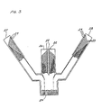
- a flexible circuit board 22 of the shape shown in FIG. 3 is used.
- the circuit board has a plurality of conductive traces 23 disposed within it, each trace having two ends. One end of each trace appears in the root 24 of the circuit board for eventual connection to the transducer array. The opposite end of each trace fans out to one of three branches of the flexible circuit board.
- the middle branch 26 is directly opposite the root of the circuit board.
- Two angled branches 27 and 28 exit at either edge of the root.
- the branches are extendable along the dashed lines 25 shown in FIG. 3. In other words, the circuit board is cut along lines 25 to extend the branches nearly down to the root 24.
- Each of the traces in each branch of the circuit board end at a connector hole 29. Each connector hole is surrounded by an exposed portion of its relative trace to form an eyelet. Separate electrical connections are thus established between each trace and a corresponding eyelet.
- each branch of the circuit board there are ninety-six conductive traces in the flexible circuit board. All ninety-six traces appear and are exposed for purposes of electrical connection at the root of the circuit board. One half of the traces flow into the middle branch of the circuit board, and one quarter of the traces flow into each of the angled branches.
- the connector holes in each branch of the circuit board are aligned in columns.
- the middle branch has two parallel columns of connector holes running down the center of that branch.
- the angled branches each have one column of connector holes aligned along the upper edge of each branch.
- the flexible circuit board 22 is positioned with respect to the array 10 such that the exposed traces at the root of the circuit board are aligned with the individual elements in the array 10.
- the curve of the root of the circuit board matches that of the array. That is, the root is bowed to allow the conductive traces to align adjacent to the elements.
- the traces in the flex board are then electrically connected to the elements in the array. More specifically, the traces in the flex board are electrically connected to the hot electrode 18 resident on each element in the transducer array.
- the electrical connection between each trace in the flexible board and the corresponding transducer array element is made by wire bonding.
- a conventional wire bonding machine is used to make the electrical connections.
- FIG. 5 shows an enlarged view of a single element 16 and the flexible circuit board 22. The trace 23 aligned with this element is electrically connected to the element with a wire bond 31. In alternative embodiments, this connection is made by reflow solder methods or micro-welding.
- an insulator material is poured into the spaces between the array elements.
- the insulator material also covers the wire bonds on each array element and thus enhances the structural integrity of the electrical connections.
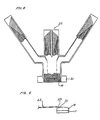
- the three branches of the flexible circuit board are then bent upward (toward the center of the arc formed by the crystal assembly) to a position approximately perpendicular to the chord of the arc formed by the array.
- the two angled branches 27 and 28 are brought together such that the eyelets in each angled branch align, and each angled branch lies in the same plane as the middle branch 26.
- the shape of the circuit board allows the branches to overlap and to create a substantially smooth 90 degree bend in the circuit board when positioned in this perpendicular orientation.
- the geometry of the angled branches 27 and 28 of the flexible circuit board 22 allows the connector holes 29 in each branch to align with each other, thus creating two parallel columns of connector holes.
- the connector hole columns in the angled branches align with the two parallel columns of connector holes in the first branch 26 of the circuit board. This creates two continuous columns of connector holes when the branches of the circuit board are bent to their perpendicular orientation.
- the upper portion of each column is formed by the connector holes in the angled branches and the lower portion of each column is formed by the connector holes in the middle branch.
- a standard pin and socket connector 33 having two parallel columns of pins 34 on one side and corresponding sockets on the opposite side is used to interface the aligned branches of the circuit board.
- the pins 34 are inserted through the connector holes 29 in the circuit board.
- the pins are then soldered to the conductive eyelets that surround each of the connector holes to establish an electrical connection between each trace and its corresponding pin.
- the transducer array 10 along with the flexible circuit board and the connector is disposed within a transducer assembly housing.
- Ground connections between the transducer array and the housing are made via radial bus wires (not shown) connected between the ground bus wires on the transducer array and the interior of the housing.
- each ground bus wire has a plurality of radial bus wires connected to it to provide for the above-described connection.
- the radial bus wires are connected to the transducer array 10 prior to the connection of the flexible circuit board to the transducer array. After the radial bus wires are connected to the array, they are bent down to a position substantially parallel to the axis of the arc formed by the curved transducer array to accommodate the connection of the flexible circuit board. Once the flexible circuit board has been connected and bent into its operative position, the radial bus wires are bent up to a position substantially parallel to the flexible circuit board to facilitate their connection to the housing.
- the sockets of the connector 33 are electrically connected to a cable which exits the transducer assembly housing and which connects the transducer assembly with the rest of the imaging apparatus.
- the cable comprises a bundle of individual wires, each of which carry signals to and from the elements of the array.
- the cable is anchored to the inside of the housing at a point along the cable between the connector 33 and the point at which the cable exits the housing. This anchor isolates the flexible circuit board and its connection to the array from tension exerted on the cable.
Abstract
A curved array ultrasonic transducer is manufactured by cutting a flat transducer plate (12), which is attached to a flexible support plate (11), into a plurality of segments (14), the segments being hingedly attached by the support plate. The support plate is bent to a radius (FIG. 2) and the conductive traces in a flexible circuit board are electrically connected to the transducer plate segments (FIG. 4). The flexible circuit board, having a plurality of branches, is bent to a perpendicular position such that the traces in the plurality of branches become substantially aligned (FIG. 6). The traces exiting the branches are then electrically connected to a pin and socket connector device (FIG. 8).
Description
- This invention generally relates to the field of ultrasonic medical transducer assemblies, and, more particularly, to a curved array ultrasonic transducer assembly having a flexible interconnect system, and a method of its manufacture.
- Ultrasonic medical transducers are used to observe the internal organs of a patient. Such an apparatus produces the display of successive images at a rapid rate so that an observer can see movements of an organ in "real time". Curved transducer arrays are used, rather than flat arrays, to enhance the performance of the ultrasonic imaging device. Principally, a curved array will produce an image over a wider field of view and thus permit the observer to view objects that would ordinarily be hidden from view when using a flat array (for example, a bone, such as a rib may obstruct the view of an internal organ).
- Typically, curved transducer arrays are fabricated by soldering a flexible circuit board to a flat transducer plate, the transducer plate generally comprising a ceramic substrate sandwiched between conductive electronic plates. A backing material is then bonded to what will become the concave surface of the array. The transducer plate is then cut into segments and subsequently formed into a curvilinear array. The backing material acts as a hinge to allow the segmented ceramic to bend while maintaining positioning between segments.
- For example, U.S. Patent No. 4,734,963 to Ishiyama discloses a method of manufacturing a curvilinear array of ultrasonic transducers wherein a flexible printed circuit board is connected to one edge of a rigid transducer plate. The transducer plate, being previously bonded to a flexible support plate, is then diced through to the support plate thus dividing the transducer plate into a series of parallel transducer elements. The support plate is then conformed to a curved shape.
- A presently preferred embodiment of the present invention provides a method of manufacturing a curved array medical transducer, whereby transducer array elements are formed by first bonding a flexible support layer to one surface of a transducer plate. The transducer plate is cut into segments, each cut penetrating only a portion of the support layer, thus forming a plurality of transducer array elements each being bonded to the support layer. The support layer is then bent to the desired radius to form a curved array of transducer elements.
- A flexible circuit board, having conductive traces disposed therein for transmitting electrical signals to and from the transducer elements, is aligned with the curved array such that the traces are adjacent to the transducer elements. The traces are then electrically connected to the transducer elements in the array.
- The conductive traces extend into a plurality of branches in the flexible circuit board. After connection of the transducer elements to the circuit board, the circuit board is bent toward the center of the array at a right angle. In doing so, conductive holes, which are associated with the ends of the conductive traces in the branches, become aligned in such a manner that a connector can be soldered to the holes in the conductive traces.
- These and other features and advantages of the present invention will be better understood by reference to the following detailed description when considered in conjunction with the accompanying drawings wherein:
- FIG. 1a is an elevational view of an exemplary transducer plate/support plate assembly;
- FIG. 1b is a sectional view of an exemplary transducer array element.
- FIG. 2 is an elevational view of a transducer array sitting in a curved tooling form;
- FIG.3 is a plan view of an exemplary flexible circuit board;
- FIG. 4 is plan view of the flexible circuit board shown in relationship to the transducer array on the tooling form;
- FIG.5 is a sectional view of a conductive trace in the circuit board in relationship to a transducer array element;
- FIG. 6 and FIG. 7 are front and side elevational views, respectively, of the circuit board in its operative position.
- FIG. 8 is a side elevational view of the circuit board shown in FIG. 7 in operative relationship to the connector.
- An exemplary
curved transducer array 10 is formed according to the following steps. First, an elongate strip ofpiezo material 8 having a substantially rectangular cross-section is completely encased in metalization such that thepiezo material 8 is surrounded on all sides byconductive material 17 thus forming atransducer plate 12 comprised of piezo-electric material. Next, two longitudinal cuts are made along the top side 15 of the transducer plate, thus forming twogrooves 9 in the transducer plate running along its length. Eachgroove 9 is deep enough to cut entirely throughconductive material 17. Accordingly, two isolated conductive areas, or electrodes, are formed. - The "hot"
electrode 18 is formed along the top surface 15 of thetransducer plate 12. Theground electrode 19 is formed along the other surfaces (bottom and sides) of the piezo material. Thegrooves 9 are cut such that theground electrode 19 slightly wraps around to the top surface 15 of the transducer plate. This provides access to both thehot electrode 18 and theground electrode 19 along the top surface of theplate 12. - A flexible support plate 11 is bonded to a the
transducer plate 12 along onesurface 13 of the transducer plate. In the embodiment described above, the support layer is bonded to the surface opposite the top surface 15 of the transducer plate to allow access to the "hot" electrode. The transducer plate is then cut intosegments 14 from top surface 15 of the transducer plate to form an array of individual transducer elements. Each cut extends into the support plate 11 but leaves a portion of the support layer uncut thus creatinghinge points 16 in the assembly, as illustrated in FIG. 1. Thetransducer plate 12 is cut into segments by means of a conventional semi-conductor dicing saw. - The
hinge points 16 allow thetransducer array 10 to be bent into an arc. The particular radius of the arc depends on the application in which the transducer will be used. - When the strip of piezo-electric material is cut into segments to form the individual transducer elements, the
ground electrode 19 andhot electrode 18 of each element is completely isolated from the electrodes of the other transducer elements. Once the transducer array is formed to the desired radius, the ground electrode of each array element is connected by soldering each of ground bus two wires (not shown) along the top edges of the array. The wires run along the top surface of the piezo-electric material in the areas where theground electrode 19 of each array element wrap around to said top surface. The ground bus wires are connected to each of the transducer elements thus forming a ground plane common to all of the elements. - Referring to FIG. 2, a
transducer array 10 formed in the manner described above, is secured in atooling form 21 of desired radius. In an exemplary embodiment, the transducer array is secured in place using adhesive tape.Segments 14 comprise the elements of thetransducer array 10. The tooling form provides support for the transducer array while it is being worked on. - In an exemplary embodiment, the top surface 15 of the transducer array will become the concave surface of the array and the support plate will become the convex surface. In use, the concave surface of the transducer array has electrical connections made to it and the convex surface is aligned to the subject to be scanned (i.e. a body part). The support layer has a thickness and impedance chosen to maximize energy transfer into the body.
- A flexible circuit board is used to connect the transducer array to a
connector device 33. In an exemplary embodiment, aflexible circuit board 22 of the shape shown in FIG. 3 is used. The circuit board has a plurality ofconductive traces 23 disposed within it, each trace having two ends. One end of each trace appears in theroot 24 of the circuit board for eventual connection to the transducer array. The opposite end of each trace fans out to one of three branches of the flexible circuit board. Themiddle branch 26 is directly opposite the root of the circuit board. Twoangled branches root 24. Each of the traces in each branch of the circuit board end at aconnector hole 29. Each connector hole is surrounded by an exposed portion of its relative trace to form an eyelet. Separate electrical connections are thus established between each trace and a corresponding eyelet. - In an exemplary embodiment, there are ninety-six conductive traces in the flexible circuit board. All ninety-six traces appear and are exposed for purposes of electrical connection at the root of the circuit board. One half of the traces flow into the middle branch of the circuit board, and one quarter of the traces flow into each of the angled branches. The connector holes in each branch of the circuit board are aligned in columns. The middle branch has two parallel columns of connector holes running down the center of that branch. The angled branches each have one column of connector holes aligned along the upper edge of each branch.
- Referring to FIG. 4, the
flexible circuit board 22 is positioned with respect to thearray 10 such that the exposed traces at the root of the circuit board are aligned with the individual elements in thearray 10. The curve of the root of the circuit board matches that of the array. That is, the root is bowed to allow the conductive traces to align adjacent to the elements. - The traces in the flex board are then electrically connected to the elements in the array. More specifically, the traces in the flex board are electrically connected to the
hot electrode 18 resident on each element in the transducer array. In an exemplary embodiment, the electrical connection between each trace in the flexible board and the corresponding transducer array element is made by wire bonding. A conventional wire bonding machine is used to make the electrical connections. FIG. 5 shows an enlarged view of asingle element 16 and theflexible circuit board 22. Thetrace 23 aligned with this element is electrically connected to the element with awire bond 31. In alternative embodiments, this connection is made by reflow solder methods or micro-welding. - In an exemplary embodiment, once all of the traces have been electrically bonded to the elements in the array, an insulator material is poured into the spaces between the array elements. The insulator material also covers the wire bonds on each array element and thus enhances the structural integrity of the electrical connections.
- The three branches of the flexible circuit board are then bent upward (toward the center of the arc formed by the crystal assembly) to a position approximately perpendicular to the chord of the arc formed by the array. The two
angled branches middle branch 26. The shape of the circuit board allows the branches to overlap and to create a substantially smooth 90 degree bend in the circuit board when positioned in this perpendicular orientation. As shown in FIGs. 6, 7 and 8, the geometry of theangled branches flexible circuit board 22 allows the connector holes 29 in each branch to align with each other, thus creating two parallel columns of connector holes. Furthermore, the connector hole columns in the angled branches align with the two parallel columns of connector holes in thefirst branch 26 of the circuit board. This creates two continuous columns of connector holes when the branches of the circuit board are bent to their perpendicular orientation. The upper portion of each column is formed by the connector holes in the angled branches and the lower portion of each column is formed by the connector holes in the middle branch. - A standard pin and
socket connector 33 having two parallel columns of pins 34 on one side and corresponding sockets on the opposite side is used to interface the aligned branches of the circuit board. The pins 34 are inserted through the connector holes 29 in the circuit board. The pins are then soldered to the conductive eyelets that surround each of the connector holes to establish an electrical connection between each trace and its corresponding pin. - In an exemplary embodiment, the
transducer array 10, along with the flexible circuit board and the connector is disposed within a transducer assembly housing. Ground connections between the transducer array and the housing are made via radial bus wires (not shown) connected between the ground bus wires on the transducer array and the interior of the housing. Accordingly, each ground bus wire has a plurality of radial bus wires connected to it to provide for the above-described connection. Typically, for a transducer array having 96 transducer elements, there are approximately fifteen radial bus wires connected to each of the two ground bus wires on the array. - The radial bus wires are connected to the
transducer array 10 prior to the connection of the flexible circuit board to the transducer array. After the radial bus wires are connected to the array, they are bent down to a position substantially parallel to the axis of the arc formed by the curved transducer array to accommodate the connection of the flexible circuit board. Once the flexible circuit board has been connected and bent into its operative position, the radial bus wires are bent up to a position substantially parallel to the flexible circuit board to facilitate their connection to the housing. - The sockets of the
connector 33 are electrically connected to a cable which exits the transducer assembly housing and which connects the transducer assembly with the rest of the imaging apparatus. The cable comprises a bundle of individual wires, each of which carry signals to and from the elements of the array. - In an exemplary embodiment, the cable is anchored to the inside of the housing at a point along the cable between the
connector 33 and the point at which the cable exits the housing. This anchor isolates the flexible circuit board and its connection to the array from tension exerted on the cable. - The preceding description has been presented with reference to the presently preferred embodiment to the invention shown in the drawings. Workers skilled in the art and technology to which this invention pertains will appreciate that alterations and changes in the described structures can be practiced without departing from the spirit, principles and scope of this invention.
- Accordingly, the foregoing description should not be read as pertaining only to the precise structure described, but rather should be read consistent with, and as support for, the following claims.
Claims (10)
- A method of connecting a flexible circuit board to a flexible array of ultrasonic transducers comprising the following steps in the sequence set forth:
bending the flexible array to a desired radius;
aligning conductive traces in the flexible circuit board with the elements of the array; and
wire bonding the traces to the elements of the curved array. - A method of manufacturing a curved array ultrasonic transducer assembly comprising the following steps in the order set forth:
bonding a flexible support layer to one surface of a transducer plate;
cutting the transducer plate into a plurality of segments while leaving a portion of the flexible support layer uncut between each segment;
bending the support layer, having the individual ceramic segments bonded thereto, to a desired radius thus forming a curved transducer array; and
electrically connecting the traces in a first end of a flexible circuit board to the transducer segments. - A method as recited in claim 2 further comprising the step of adding insulating material between the ceramic segments and over the electrical connections following the step whereby the traces are electrically connected to the transducer segments.
- A method as recited in claim 2 wherein the electrically connecting step comprises wire bonding the traces in the flexible circuit board to the ceramic elements.
- A method as recited in claim 2 further comprising the steps of:
bending the flexible circuit board toward the center of the arc formed by the curved transducer assembly such that it is substantially perpendicular to the chord of the formed arc; and
electrically connecting a connector to the traces at a second end of the flexible circuit board. - A method as recited in claim 5 wherein the flexible circuit board has conductive traces disposed within it which begin at the first end of the circuit board and end at the second end of the circuit board.
- A method as recited in claim 6 wherein the second end of the flexible circuit board comprises a plurality of branches.
- A method as recited in claim 7 wherein the ends of the conductive traces in each branch substantially align with each other when the flexible circuit board is bent in the perpendicular orientation.
- A method as recited in claim 5 wherein the transducer plate is formed by a method comprising the following steps:
encasing an elongate strip of piezo material in a conductive material; and
cutting two longitudinal groves along the elongate strip thus separating the conductive layer into two separate areas, each being electrically isolated. - A method as recited in claim 9 wherein the grooves are cut along a common longitudinal edge.
Applications Claiming Priority (2)
| Application Number | Priority Date | Filing Date | Title |
|---|---|---|---|
| US07/526,569 US5044053A (en) | 1990-05-21 | 1990-05-21 | Method of manufacturing a curved array ultrasonic transducer assembly |
| US526569 | 1990-05-21 |
Publications (2)
| Publication Number | Publication Date |
|---|---|
| EP0458092A2 true EP0458092A2 (en) | 1991-11-27 |
| EP0458092A3 EP0458092A3 (en) | 1993-01-20 |
Family
ID=24097868
Family Applications (1)
| Application Number | Title | Priority Date | Filing Date |
|---|---|---|---|
| EP19910106978 Withdrawn EP0458092A3 (en) | 1990-05-21 | 1991-04-30 | Curved array ultrasonic transducer assembly and its method of manufacture |
Country Status (3)
| Country | Link |
|---|---|
| US (1) | US5044053A (en) |
| EP (1) | EP0458092A3 (en) |
| JP (1) | JPH0629072A (en) |
Cited By (3)
| Publication number | Priority date | Publication date | Assignee | Title |
|---|---|---|---|---|
| WO2003011141A1 (en) * | 2001-07-31 | 2003-02-13 | Koninklijke Philips Electronics N.V. | Ultrasound probe wiring method and apparatus |
| EP1534136A2 (en) * | 2002-08-29 | 2005-06-01 | Volcano Therapeutics, Inc. | Ultrasonic imaging devices and methods of fabrication |
| US7514851B2 (en) * | 2005-07-13 | 2009-04-07 | Siemens Medical Solutions Usa, Inc. | Curved capacitive membrane ultrasound transducer array |
Families Citing this family (29)
| Publication number | Priority date | Publication date | Assignee | Title |
|---|---|---|---|---|
| FR2691596B1 (en) * | 1992-05-22 | 1995-04-28 | Thomson Csf | Acoustic underwater antenna with area sensor. |
| AU5017393A (en) * | 1992-08-18 | 1994-03-15 | Kinesis Corporation | Keyboard and method for producing |
| US5423220A (en) * | 1993-01-29 | 1995-06-13 | Parallel Design | Ultrasonic transducer array and manufacturing method thereof |
| US5453575A (en) * | 1993-02-01 | 1995-09-26 | Endosonics Corporation | Apparatus and method for detecting blood flow in intravascular ultrasonic imaging |
| US5398689A (en) * | 1993-06-16 | 1995-03-21 | Hewlett-Packard Company | Ultrasonic probe assembly and cable therefor |
| US5428190A (en) * | 1993-07-02 | 1995-06-27 | Sheldahl, Inc. | Rigid-flex board with anisotropic interconnect and method of manufacture |
| US5792058A (en) * | 1993-09-07 | 1998-08-11 | Acuson Corporation | Broadband phased array transducer with wide bandwidth, high sensitivity and reduced cross-talk and method for manufacture thereof |
| US5527998A (en) * | 1993-10-22 | 1996-06-18 | Sheldahl, Inc. | Flexible multilayer printed circuit boards and methods of manufacture |
| GB2287375B (en) | 1994-03-11 | 1998-04-15 | Intravascular Res Ltd | Ultrasonic transducer array and method of manufacturing the same |
| US5719749A (en) * | 1994-09-26 | 1998-02-17 | Sheldahl, Inc. | Printed circuit assembly with fine pitch flexible printed circuit overlay mounted to printed circuit board |
| JP3487981B2 (en) * | 1994-10-20 | 2004-01-19 | オリンパス株式会社 | Ultrasonic probe |
| US5706820A (en) * | 1995-06-07 | 1998-01-13 | Acuson Corporation | Ultrasonic transducer with reduced elevation sidelobes and method for the manufacture thereof |
| US7226417B1 (en) | 1995-12-26 | 2007-06-05 | Volcano Corporation | High resolution intravascular ultrasound transducer assembly having a flexible substrate |
| US5735282A (en) * | 1996-05-30 | 1998-04-07 | Acuson Corporation | Flexible ultrasonic transducers and related systems |
| US5680863A (en) * | 1996-05-30 | 1997-10-28 | Acuson Corporation | Flexible ultrasonic transducers and related systems |
| US5857974A (en) | 1997-01-08 | 1999-01-12 | Endosonics Corporation | High resolution intravascular ultrasound transducer assembly having a flexible substrate |
| JP4408974B2 (en) * | 1998-12-09 | 2010-02-03 | 株式会社東芝 | Ultrasonic transducer and manufacturing method thereof |
| JP2001210921A (en) * | 2000-01-28 | 2001-08-03 | Mitsumi Electric Co Ltd | Printed board |
| US6468221B2 (en) * | 2000-11-21 | 2002-10-22 | Asahi Kogaku Kogyo Kabushiki Kaisha | Ultrasonic endoscope |
| JP3579646B2 (en) * | 2000-11-21 | 2004-10-20 | ペンタックス株式会社 | Ultrasound endoscope |
| JP3579651B2 (en) * | 2000-11-21 | 2004-10-20 | ペンタックス株式会社 | Ultrasound endoscope |
| US7806827B2 (en) * | 2003-03-11 | 2010-10-05 | General Electric Company | Ultrasound breast screening device |
| DE102006010009A1 (en) * | 2006-03-04 | 2007-09-13 | Intelligendt Systems & Services Gmbh & Co Kg | A method of manufacturing an ultrasonic probe with an ultrasonic transducer assembly having a curved transmitting and receiving surface |
| USD585063S1 (en) | 2007-11-27 | 2009-01-20 | Kinesis Corporation | Keyboard |
| EP2114085A1 (en) * | 2008-04-28 | 2009-11-04 | Nederlandse Centrale Organisatie Voor Toegepast Natuurwetenschappelijk Onderzoek TNO | Composite microphone, microphone assembly and method of manufacturing those |
| US20100171395A1 (en) * | 2008-10-24 | 2010-07-08 | University Of Southern California | Curved ultrasonic array transducers |
| US8479585B2 (en) | 2010-09-08 | 2013-07-09 | Micropen Technologies Corporation | Pressure sensing or force generating device |
| KR102607016B1 (en) * | 2018-01-31 | 2023-11-29 | 삼성메디슨 주식회사 | Ultrasonic probe |
| US11792933B2 (en) * | 2021-07-29 | 2023-10-17 | Fermi Research Alliance, Llc | Connector interface assembly for enclosed vessels and associated systems and methods |
Citations (8)
| Publication number | Priority date | Publication date | Assignee | Title |
|---|---|---|---|---|
| JPS52123265A (en) * | 1976-04-08 | 1977-10-17 | Oki Electric Ind Co Ltd | Ultrasonic transmitting and receiving device |
| JPS54149615A (en) * | 1978-05-17 | 1979-11-24 | Oki Electric Ind Co Ltd | Production of ultrasonic oscillator of curved arrangement type |
| JPS57188195A (en) * | 1981-05-14 | 1982-11-19 | Yokogawa Hokushin Electric Corp | Manufacture for conformal array oscillator |
| EP0145429A2 (en) * | 1983-12-08 | 1985-06-19 | Kabushiki Kaisha Toshiba | Curvilinear array of ultrasonic transducers |
| JPS6132698A (en) * | 1984-07-25 | 1986-02-15 | Toshiba Corp | Manufacture of ultrasonic probe |
| JPS6175700A (en) * | 1984-09-21 | 1986-04-18 | Toshiba Corp | Ultrasonic probe and its manufacture |
| EP0351015A2 (en) * | 1988-07-15 | 1990-01-17 | Koninklijke Philips Electronics N.V. | A method for fabricating a piezoelectric composite transducer |
| US4894895A (en) * | 1987-02-24 | 1990-01-23 | Kabushiki Kaisha Toshiba | Method of making an ultrasonic probe |
-
1990
- 1990-05-21 US US07/526,569 patent/US5044053A/en not_active Expired - Fee Related
-
1991
- 1991-04-30 EP EP19910106978 patent/EP0458092A3/en not_active Withdrawn
- 1991-05-16 JP JP3141078A patent/JPH0629072A/en active Pending
Patent Citations (8)
| Publication number | Priority date | Publication date | Assignee | Title |
|---|---|---|---|---|
| JPS52123265A (en) * | 1976-04-08 | 1977-10-17 | Oki Electric Ind Co Ltd | Ultrasonic transmitting and receiving device |
| JPS54149615A (en) * | 1978-05-17 | 1979-11-24 | Oki Electric Ind Co Ltd | Production of ultrasonic oscillator of curved arrangement type |
| JPS57188195A (en) * | 1981-05-14 | 1982-11-19 | Yokogawa Hokushin Electric Corp | Manufacture for conformal array oscillator |
| EP0145429A2 (en) * | 1983-12-08 | 1985-06-19 | Kabushiki Kaisha Toshiba | Curvilinear array of ultrasonic transducers |
| JPS6132698A (en) * | 1984-07-25 | 1986-02-15 | Toshiba Corp | Manufacture of ultrasonic probe |
| JPS6175700A (en) * | 1984-09-21 | 1986-04-18 | Toshiba Corp | Ultrasonic probe and its manufacture |
| US4894895A (en) * | 1987-02-24 | 1990-01-23 | Kabushiki Kaisha Toshiba | Method of making an ultrasonic probe |
| EP0351015A2 (en) * | 1988-07-15 | 1990-01-17 | Koninklijke Philips Electronics N.V. | A method for fabricating a piezoelectric composite transducer |
Non-Patent Citations (5)
| Title |
|---|
| PATENT ABSTRACTS OF JAPAN vol. 10, no. 186 (E-416)(2242) 28 June 1986 & JP-A-61 32 698 ( TOSHIBA CORP ) 15 February 1986 * |
| PATENT ABSTRACTS OF JAPAN vol. 10, no. 248 (E-431)26 August 1986 & JP-A-61 75 700 ( TOSHIBA CORP ) 18 April 1986 * |
| PATENT ABSTRACTS OF JAPAN vol. 2, no. 007 (E-005)18 January 1978 & JP-A-52 123 265 ( OKI DENKI KOGYO K.K. ) 17 October 1977 * |
| PATENT ABSTRACTS OF JAPAN vol. 4, no. 10 (E-167)25 January 1980 & JP-A-54 149 615 ( OKI DENKI KOGYO K.K. ) 24 November 1979 * |
| PATENT ABSTRACTS OF JAPAN vol. 7, no. 36 (E-158)15 February 1983 & JP-A-57 188 195 ( YOKOGAWA DENKI SEISAKUSHO KK ) 19 November 1982 * |
Cited By (5)
| Publication number | Priority date | Publication date | Assignee | Title |
|---|---|---|---|---|
| WO2003011141A1 (en) * | 2001-07-31 | 2003-02-13 | Koninklijke Philips Electronics N.V. | Ultrasound probe wiring method and apparatus |
| EP1534136A2 (en) * | 2002-08-29 | 2005-06-01 | Volcano Therapeutics, Inc. | Ultrasonic imaging devices and methods of fabrication |
| EP1534136A4 (en) * | 2002-08-29 | 2006-05-10 | Volcano Therapeutics Inc | Ultrasonic imaging devices and methods of fabrication |
| US7514851B2 (en) * | 2005-07-13 | 2009-04-07 | Siemens Medical Solutions Usa, Inc. | Curved capacitive membrane ultrasound transducer array |
| US7732992B2 (en) | 2005-07-13 | 2010-06-08 | Siemens Medical Solutions Usa, Inc. | Curved capacitive membrane ultrasound transducer array |
Also Published As
| Publication number | Publication date |
|---|---|
| JPH0629072A (en) | 1994-02-04 |
| EP0458092A3 (en) | 1993-01-20 |
| US5044053A (en) | 1991-09-03 |
Similar Documents
| Publication | Publication Date | Title |
|---|---|---|
| US5044053A (en) | Method of manufacturing a curved array ultrasonic transducer assembly | |
| US4404489A (en) | Acoustic transducer with flexible circuit board terminals | |
| US6952870B2 (en) | Integrated circuit wiring method | |
| JP2545861B2 (en) | Ultrasonic probe manufacturing method | |
| US5449862A (en) | Planar cable array | |
| US6100626A (en) | System for connecting a transducer array to a coaxial cable in an ultrasound probe | |
| US6859984B2 (en) | Method for providing a matrix array ultrasonic transducer with an integrated interconnection means | |
| US4435614A (en) | Elongated printed circuit flexible cables and method of making the same | |
| US4894895A (en) | Method of making an ultrasonic probe | |
| JPS60227373A (en) | Multicontact connector and method of producing same | |
| US20080129152A1 (en) | Cable direct interconnection (cdi) method for phased array transducers | |
| CA1139858A (en) | Flat cable assembly and methods of terminating and connectorizing the cable of same | |
| JP2004112326A (en) | Ultrasonic probe and its manufacturing method | |
| JP6010259B1 (en) | Ultrasonic transducer, ultrasonic endoscope | |
| JPH03270500A (en) | Ultrasonic probe and manufacture thereof | |
| JPH04179074A (en) | Method for connecting multi-core cable | |
| JP3934202B2 (en) | Ultrasonic probe | |
| JPH0553119B2 (en) | ||
| JP3661261B2 (en) | Flat cable | |
| JP2002153461A (en) | Ultrasonic vibrator and manufacturing method therefor | |
| JP4492773B2 (en) | Multi-core coaxial cable connection terminal and manufacturing method thereof | |
| JP2689532B2 (en) | Ultrasonic probe manufacturing method | |
| JPS6132698A (en) | Manufacture of ultrasonic probe | |
| JPS63146699A (en) | Manufacture of two-dimension array transducer | |
| JPS5919518Y2 (en) | ultrasonic probe |
Legal Events
| Date | Code | Title | Description |
|---|---|---|---|
| PUAI | Public reference made under article 153(3) epc to a published international application that has entered the european phase |
Free format text: ORIGINAL CODE: 0009012 |
|
| AK | Designated contracting states |
Kind code of ref document: A2 Designated state(s): DE FR GB IT |
|
| PUAL | Search report despatched |
Free format text: ORIGINAL CODE: 0009013 |
|
| AK | Designated contracting states |
Kind code of ref document: A3 Designated state(s): DE FR GB IT |
|
| STAA | Information on the status of an ep patent application or granted ep patent |
Free format text: STATUS: THE APPLICATION HAS BEEN WITHDRAWN |
|
| 18W | Application withdrawn |
Withdrawal date: 19930717 |