EP0457932A1 - Circuit arrangement for band switching in tuners - Google Patents
Circuit arrangement for band switching in tuners Download PDFInfo
- Publication number
- EP0457932A1 EP0457932A1 EP90109584A EP90109584A EP0457932A1 EP 0457932 A1 EP0457932 A1 EP 0457932A1 EP 90109584 A EP90109584 A EP 90109584A EP 90109584 A EP90109584 A EP 90109584A EP 0457932 A1 EP0457932 A1 EP 0457932A1
- Authority
- EP
- European Patent Office
- Prior art keywords
- terminal
- switching
- circuit arrangement
- potential terminal
- mos
- Prior art date
- Legal status (The legal status is an assumption and is not a legal conclusion. Google has not performed a legal analysis and makes no representation as to the accuracy of the status listed.)
- Granted
Links
- 230000003321 amplification Effects 0.000 claims abstract description 5
- 238000003199 nucleic acid amplification method Methods 0.000 claims abstract description 5
- 230000008878 coupling Effects 0.000 claims description 5
- 238000010168 coupling process Methods 0.000 claims description 5
- 238000005859 coupling reaction Methods 0.000 claims description 5
- 230000001681 protective effect Effects 0.000 claims description 2
- 239000003990 capacitor Substances 0.000 description 3
- 230000000694 effects Effects 0.000 description 1
Images

Classifications
-
- H—ELECTRICITY
- H03—ELECTRONIC CIRCUITRY
- H03J—TUNING RESONANT CIRCUITS; SELECTING RESONANT CIRCUITS
- H03J5/00—Discontinuous tuning; Selecting predetermined frequencies; Selecting frequency bands with or without continuous tuning in one or more of the bands, e.g. push-button tuning, turret tuner
- H03J5/24—Discontinuous tuning; Selecting predetermined frequencies; Selecting frequency bands with or without continuous tuning in one or more of the bands, e.g. push-button tuning, turret tuner with a number of separate pretuned tuning circuits or separate tuning elements selectively brought into circuit, e.g. for waveband selection or for television channel selection
- H03J5/242—Discontinuous tuning; Selecting predetermined frequencies; Selecting frequency bands with or without continuous tuning in one or more of the bands, e.g. push-button tuning, turret tuner with a number of separate pretuned tuning circuits or separate tuning elements selectively brought into circuit, e.g. for waveband selection or for television channel selection used exclusively for band selection
- H03J5/244—Discontinuous tuning; Selecting predetermined frequencies; Selecting frequency bands with or without continuous tuning in one or more of the bands, e.g. push-button tuning, turret tuner with a number of separate pretuned tuning circuits or separate tuning elements selectively brought into circuit, e.g. for waveband selection or for television channel selection used exclusively for band selection using electronic means
Definitions
- the invention relates to a circuit arrangement for range switching in tuners with the features of the preamble of claim 1.
- Television tuners usually contain two or three tuners that are operated electrically largely independently of one another and cover the television frequency ranges in the VHF bands and in the UHF band.
- Hyperband tuners i.e. tuners that also cover the hyperband distributed in cable networks with the frequency range 300 to 470 MHz, generally consist of three electrically independent sub-tuners.
- the band or range switching of the tuned resonant circuits is generally not carried out with switch diodes because of the large frequency ranges to be tuned.
- switch diodes are used directly at the antenna input, which only switch the currently selected area to the antenna connection of the television set. The switchover of the tuners and the switch diodes takes place - as described above - by means of switch transistors.
- an integrated circuit which contains a mixer and an oscillator for each sub-area.
- a switching device is also integrated into this integrated circuit, which switches on the desired mixer and oscillator by applying a specific control signal, for example voltage level.
- the control signal can be derived, for example, from appropriately designed voltage dividers from switched-over operating voltages for the part tuners.
- the switch transistors only switch the current of the switch diodes and the operating voltage of the pre-stages of the tuner, into which MOS tetrodes are usually used to amplify the high frequency.
- Two circuit arrangements for area switching in television tuners with MOS tetrodes and an integrated circuit for VHF / UHF switching are shown, for example, on pages 767 and 768 of the Siemens data book 1986/87 "ICs for Consumer Electronics".
- a hyperband tuner known as Philips UV 816 which does not require switch transistors. This is achieved by an integrated switching device with non-current-limited switching outputs, via which the first gate connections of the non-switched-on MOS tetrodes are switched to ground. As a result, these MOS tetrodes become currentless and lose their amplification. Only the MOS tetrode of the active area remains switched on, since the switching output of the integrated switching device provided for this remains high-resistance and thus inactive. The disadvantage of this principle is: Such a tuner requires a control device for its control, that is, for. B.
- the invention is therefore based on the object of specifying a circuit arrangement for range switching in tuners which is functionally and software-compatible with the previous tuners and whose circuit complexity and space requirement is reduced compared to the previously known circuits.
- the input stage has three preliminary stages 1, 1 ′ and 1 ′′ with MOS tetrodes 4 for amplifying an antenna signal to be applied to a terminal 20.
- this antenna signal Via a coupling member 21, for. B. a coupling capacitor, this antenna signal reaches the Cathodes of three switch diodes 37, 37 'and 37'', the anodes of which are connected to an input terminal 7, 7', 7 '' of the preliminary stages 1, 1 'and 1''.
- At their output terminals 8, 8 'and 8''a high frequency amplified signal can be tapped for each area of the respective preamplifier 1, 1' and 1 ''.
- preliminary stage 1 for a first area, here z. B. the VHF I area with its individual circuit components shown in detail, as they are known from the Siemens data book 1986/87 mentioned above. The circuit arrangement is therefore only dealt with in the following to the extent that it is necessary for an understanding of the invention.
- the source connection S of the MOS tetrode 4 is connected to the connection point of a first voltage divider 15 and the first gate connection G1 is connected to the connection point of a second voltage divider 16 for setting the operating point.
- Both voltage dividers 15 and 16 are located between a reference potential terminal 6 and a terminal 43, which can be switched via a pnp switching transistor 40 to a supply potential terminal 5 with an applied positive voltage.
- the collector connection of this pnp switching transistor 40 with the terminal 43 and its base connection is connected via a base resistor 42 to a switching output 14 of a switching device 9.
- the emitter connection of the pnp switching transistor 40 is connected on the one hand via an emitter resistor 41 to the base connection of the pnp switching transistor 40 and on the other hand to the supply potential terminal 5.
- the switching output 14 of the switching device 9 is controlled via one or more control connections 11 by means of one or more control signals.
- the anode of the switch diode 37 is connected to the terminal 43 of the preliminary stage 1 via a resistor 39.
- the switching output 14 of the switching device 9 is switched to low impedance when the VHF I range is selected by operating elements in the television set, that is to say to reference potential, the pnp switching transistor switches 40 a.
- the positive voltage at the supply potential terminal 5 thus reaches the terminal 43, as a result of which the preliminary stage 1 is connected to the positive voltage and is thus activated.
- the switch diode 37 becomes conductive since its cathode is now more negative than its anode.
- the current for switching this switch diode 37 is provided by the pnp switching transistor 40.
- the antenna signal present at the terminal 20 and to be amplified is thus amplified in the preamplifier 1 and is available at the output terminal 8.
- Switching to the other areas, here the two pre-stages 1 'and 1' 'for the VHF II and UHF areas, is carried out in an analogous manner via the switching outputs 14' and 14 '' of the switching device 9, as well as by means of the Reference numerals 7 ', 37', 40 ', 41', 42 'and 43' and 7 '', 37 '', 40 '', 41 '', 42 '' and 43 '' designated circuit components is shown.
- the same digits of the reference symbols denote analog switching elements.
- preamplifier 1' With low-impedance switching output 14 ', preamplifier 1' thus becomes active, while with low-impedance switching output 14 '', preamplifier 1 '' is connected to supply potential terminal 5 via the then switched on pnp switching transistor 40 '' and thus works as an amplifier.
- the switching outputs 14, 14 'and 14' 'of the switching device 9 are current-limited open collector outputs.
- a current limitation in the switching device 9 prevents the base current of the pnp switching transistors 40, 40 'and 40' 'from being too high.
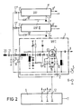
- FIG. 2 shows an exemplary embodiment of a circuit arrangement according to the invention for range switching in tuners.
- the same reference numerals as in FIG 1 indicate the same circuit elements.
- the source terminal S of the MOS tetrode 4 is connected via a resistor 10 and the terminal 2 to a switching output 12 of the switching device 9.
- this switching output 12 of the switching device 9 can be switched to reference potential and thus connected to the reference potential terminal 6, whereby the MOS tetrode 4 and thus the preliminary stage 1 can be activated is.
- the MOS tetrode 4 So that the MOS tetrode 4 is switched off when the switching output 12 is not at reference potential, two voltage dividers which are matched to one another and connected between the supply potential terminal 5 and the reference potential terminal 6 are connected to the MOS tetrode 4.
- the first voltage divider 15, for example consisting of two resistors, is connected with its connection point to the source connection S and the second voltage divider 16, for example consisting of two resistors, is connected with its connection point to a first gate connection G1 of the MOS tetrode 4.
- the first voltage divider 15 and second voltage divider 16 are set so that a negative voltage is reached at the source terminal S of the MOS tetrode 4, which is large enough on the one hand to pinch off a channel forming in the MOS tetrode 4 and on the other hand below the response threshold of protective diodes connected to the first gate terminal G1 and second gate terminal G2 of the MOS tetrode 4 remains.
- the MOS tetrode 4 is currentless and RF amplification is not possible.
- the pre-stage 1 is to be activated, the switching output 12 of the switching device 9 is switched to reference potential in accordance with one or more control signals to be applied to one or more input terminals 11 of the switching device 9 and thus the source connection S of the MOS tetrode 4 via the resistor 10 with the Reference potential terminal 6 connected.
- This resistor 10, which is connected in parallel with a resistor of the first voltage divider 15, is advantageously dimensioned such that the operating point of the MOS tetrode 4 provided for optimum amplification is established.
- the aforementioned switch diode 17 is provided and connected with its cathode to the input terminal 7 of the preamplifier 1 and via a resistor 18, which is high-ohmic in comparison to the input impedance of the preamplifier 1, to the switching output 12 of the switching device 9 is connected and that a third voltage divider 19 connected between the supply potential terminal 5 and reference potential terminal 6 is provided, which is connected with its connection point to the anode of the switch diode 17.
- This measure has the effect that - as long as the switching output 12 is not at reference potential - the switch diode 17 blocks and therefore no antenna signal reaches the input terminal 7 of the preamplifier 1.
- the switch diode 17 blocks this area since the anode of the switch diode 17 is more negative than the cathode due to the third voltage divider 19, which is connected via a resistor 18 connected between the cathode of the switch diode 17 and the switching output 12 and the resistor 10 at the source connection S of the MOS Tetrode 4 lies.
- switch diode 17 carries current since its anode potential becomes more positive than its cathode potential.
- the further pre-stages 1 'and 1''of the remaining areas provided in the tuner can - as shown in FIG. 2 - be connected in the same way to further switching outputs 12' and 12 '' of the switching device 9 and to via further switch diodes 17 'and 17'' the coupling capacitor 21 of the antenna input terminal 20 are switched.
- the switching outputs 12 'and 12'' are to be connected to the terminals 2' and 2 '' of the preamplifiers 1 'and 1'', which in turn are each connected via a resistor to the source connection of the respective MOS tetrode of the preamplifiers 1' and 1 '' are connected.
- An integrated circuit is particularly suitable as the switching device 9, the switching outputs 12, 12 ′ and 12 ′′ necessary for the range switching need not have any current limitation. It is particularly advantageous that the control of the switching outputs 12, 12 'and 12' 'can be designed to be compatible with the control software of the previous tuners.
- the switching device 9 can also be included, for example, in an integrated PLL (phase-locked-loop) circuit which, for. B. has all the stages necessary for frequency adjustment and band switching.
- switching transistors provided in the switching device 9 for driving the switching outputs 12, 12 'and 12' ' should be dimensioned such that they can switch a current of about 25 mA at a dielectric strength of about 12 V.
- the principle of the present invention and thus the switching off of a preliminary stage via the source potential of a MOS tetrode is suitable for all tuners, in particular those with VHF resonant circuits which can be switched over with switch diodes but also those which work without switch diodes.
- the most important advantage of the invention lies in the fact that the circuit arrangement for switching the range of the tuner to the previous circuit arrangements is functionally and software-compatible and its circuit complexity and space requirements are reduced compared to the previously known circuit arrangements.
Landscapes
- Channel Selection Circuits, Automatic Tuning Circuits (AREA)
- Input Circuits Of Receivers And Coupling Of Receivers And Audio Equipment (AREA)
- Circuits Of Receivers In General (AREA)
- Electronic Switches (AREA)
- Circuit For Audible Band Transducer (AREA)
- Pharmaceuticals Containing Other Organic And Inorganic Compounds (AREA)
- Networks Using Active Elements (AREA)
- Oscillators With Electromechanical Resonators (AREA)
- Amplifiers (AREA)
Abstract
Description
Die Erfindung betrifft eine Schaltungsanordnung zur Bereichsumschaltung in Tunern mit den Merkmalen des Oberbegriffs des Anspruches 1.The invention relates to a circuit arrangement for range switching in tuners with the features of the preamble of claim 1.
In Fernsehtunern sind üblicherweise zwei oder drei elektrisch weitgehend unabhängig voneinander betriebene Teiltuner enthalten, die die Fernsehfrequenzbereiche in den VHF-Bändern und im UHF-Band abdecken.Television tuners usually contain two or three tuners that are operated electrically largely independently of one another and cover the television frequency ranges in the VHF bands and in the UHF band.
Herkömmliche Tuner benutzen für die zwei oder drei VHF-Bereiche gemeinsame Schwingkreise, deren Teilinduktivitäten für die Bereichsumschaltung mittels gleichspannungsgesteuerter Schalterdioden umgeschaltet werden. Die Umschaltung zwischen dem VHF- und dem UHF-Bereich wird mittels pnp-Schaltertransistoren durchgeführt, die mit ihren Emittern an die Versorgungsspannungsklemme geschaltet sind und an deren Kollektoren die Teiltuner liegen. Die Basisanschlüsse sind mit Schaltausgängen einer integrierten Schaltung, im allgemeinen einer PLL-Schaltung, verbunden. Diese Schaltausgänge sind strombegrenzte Open-Kollektor-Ausgänge, die bei der Auswahl eines Bereichs durch die Bedienelemente des Fernsehgerätes niederohmig werden und über den entsprechenden Schaltertransistor den Teiltuner mit Spannung versorgen. Eine interne Strombegrenzung in der integrierten Schaltung verhindert dabei einen zu hohen Basisstrom des Schaltertransistors. Die Umschaltung der VHF-Bereiche erfolgt dadurch, daß der von der integrierten Schaltung angesteuerte Schaltertransistor die zur Aktivierung der Schalterdioden notwendigen Ströme aufbringt.Conventional tuners use common resonant circuits for the two or three VHF ranges, the partial inductances of which are switched for the range switching by means of DC-controlled switch diodes. The switchover between the VHF and the UHF range is carried out by means of pnp switch transistors, which are connected to the supply voltage terminal with their emitters and on whose collectors the tuners are located. The base connections are connected to switching outputs of an integrated circuit, generally a PLL circuit. These switching outputs are current-limited open collector outputs, which become low-impedance when the user selects an area using the controls on the television, and which supply the part-tuner with voltage via the corresponding switch transistor. An internal current limitation in the integrated circuit prevents the base current of the switch transistor from being too high. The switchover of the VHF ranges takes place in that the switch transistor driven by the integrated circuit applies the currents necessary to activate the switch diodes.
Hyperbandtuner, also Tuner die auch das in Kabelnetzen verteilte Hyperband mit dem Frequenzbereich 300 bis 470 MHz abdecken, bestehen in der Regel aus drei elektrisch unabhängigen Teiltunern. Die Band- oder Bereichsumschaltung der abgestimmten Schwingkreise wird wegen der großen abzustimmenden Frequenzbereiche in der Regel nicht mit Schalterdioden durchgeführt. Dagegen werden direkt am Antenneneingang Schalterdioden eingesetzt, die nur den gerade ausgewählten Bereich an den Antennenanschluß des Fernsehgerätes schalten. Die Umschaltung der Teiltuner und der Schalterdioden erfolgt - wie oben beschrieben - mittels Schaltertransistoren.Hyperband tuners, i.e. tuners that also cover the hyperband distributed in cable networks with the frequency range 300 to 470 MHz, generally consist of three electrically independent sub-tuners. The band or range switching of the tuned resonant circuits is generally not carried out with switch diodes because of the large frequency ranges to be tuned. In contrast, switch diodes are used directly at the antenna input, which only switch the currently selected area to the antenna connection of the television set. The switchover of the tuners and the switch diodes takes place - as described above - by means of switch transistors.
In vielen Hyperbandtunern wird heute eine integrierte Schaltung eingesetzt, die für jeden Teilbereich einen Mischer und einen Oszillator enthält. In diese integrierte Schaltung ist auch eine Schalteinrichtung integriert, die durch Anlegen eines bestimmten Steuersignales, beispielsweise Spannungspegels, den gewünschten Mischer und Oszillator einschaltet. Das Steuersignal kann beispielsweise über entsprechend ausgelegte Spannungsteiler aus umgeschalteten Betriebsspannungen für die Teiltuner abgeleitet werden. Die Schaltertransistoren schalten in diesem Fall nur noch den Strom der Schalterdioden und die Betriebsspannung der Vorstufen des Tuners, in die üblicherweise MOS-Tetroden zur Verstärkung der Hochfrequenz eingesetzt werden. Zwei Schaltungsanordnungen zur Bereichsumschaltung in Fernsehtunern mit MOS-Tetroden und einer integrierten Schaltung zur VHF/UHF-Umschaltung sind beispielsweise auf den Seiten 767 und 768 des Siemens Datenbuches 1986/87 "ICs für die Unterhaltungselektronik" gezeigt.In many hyperband tuners today an integrated circuit is used, which contains a mixer and an oscillator for each sub-area. A switching device is also integrated into this integrated circuit, which switches on the desired mixer and oscillator by applying a specific control signal, for example voltage level. The control signal can be derived, for example, from appropriately designed voltage dividers from switched-over operating voltages for the part tuners. In this case, the switch transistors only switch the current of the switch diodes and the operating voltage of the pre-stages of the tuner, into which MOS tetrodes are usually used to amplify the high frequency. Two circuit arrangements for area switching in television tuners with MOS tetrodes and an integrated circuit for VHF / UHF switching are shown, for example, on pages 767 and 768 of the Siemens data book 1986/87 "ICs for Consumer Electronics".
Darüber hinaus ist ein Hyperbandtuner unter der Bezeichnung UV 816 von Philips bekannt, der keine Schaltertransistoren benötigt. Dies wird durch eine integrierte Schalteinrichtung mit nicht strombegrenzten Schaltausgängen erreicht, über die die ersten Gateanschlüsse der nicht eingeschalteten MOS-Tetroden auf Masse geschaltet werden. Damit werden diese MOS-Tetroden stromlos und verlieren ihre Verstärkung. Nur die MOS-Tetrode des aktiven Bereichs bleibt eingeschaltet, indem der dafür vorgesehene Schaltausgang der integrierten Schalteinrichtung hochohmig und damit inaktiv bleibt. Nachteilig bei diesem Prinzip ist:
Ein solcher Tuner benötigt zu seiner Steuerung eine Steuereinrichtung, also z. B. einen Mikroprozessor des Fernsehgerätes, mit einer anderen Software als bei den bisher benutzten oben beschriebenen Tunern, da einerseits andere Schaltausgänge der integrierten Schalteinrichtung notwendig und andererseits eine in ihrer Polarität entgegengesetzte Schaltlogik eingesetzt werden muß. Damit ist ein solcher Tuner zu den bisher bekannten Tunern nicht kompatibel.In addition, a hyperband tuner known as Philips UV 816 is known, which does not require switch transistors. This is achieved by an integrated switching device with non-current-limited switching outputs, via which the first gate connections of the non-switched-on MOS tetrodes are switched to ground. As a result, these MOS tetrodes become currentless and lose their amplification. Only the MOS tetrode of the active area remains switched on, since the switching output of the integrated switching device provided for this remains high-resistance and thus inactive. The disadvantage of this principle is:
Such a tuner requires a control device for its control, that is, for. B. a microprocessor of the television, with a different software than in the previously used tuners described above, since on the one hand other switching outputs of the integrated switching device are necessary and on the other hand, a switching logic with opposite polarity must be used. This means that such a tuner is not compatible with the previously known tuners.
Die von diesen Tunern benutzten Schaltausgänge der integrierten Schaltung können nicht zusätzlich - entgegen dem heute üblichen Standard - für Schaltaufgaben außerhalb des Tuners genutzt werden.The switching outputs of the integrated circuit used by these tuners cannot be used for switching tasks outside the tuner, contrary to the standard that is common today.
Der Erfindung liegt deshalb die Aufgabe zugrunde, eine Schaltungsanordnung zur Bereichsumschaltung in Tunern anzugeben, die mit den bisherigen Tunern funktions- und softwarekompatibel und deren Schaltungsaufwand und Platzbedarf gegenüber den bisher bekannten Schaltungen reduziert ist.The invention is therefore based on the object of specifying a circuit arrangement for range switching in tuners which is functionally and software-compatible with the previous tuners and whose circuit complexity and space requirement is reduced compared to the previously known circuits.
Die Erfindung wird im folgenden anhand von zwei Figuren beispielhaft für die Bereichsumschaltung zum VHF I-Bereich näher erläutert. Für die anderen Bereiche, z. B. VHF II und UHF, sind die Schaltungsanordnungen analog aufgebaut. Es zeigen:
- FIG 1
- eine bekannte Schaltungsanordnung zur Bereichsumschaltung in Tunern mit Schaltertransistoren und
- FIG 2
- eine erfindungsgemäße Schaltungsanordnung zur Bereichsumschaltung in Tunern mit MOS-Tetroden, deren Sourceanschlüsse auf Bezugspotential schaltbar sind.
- FIG. 1
- a known circuit arrangement for range switching in tuners with switch transistors and
- FIG 2
- a circuit arrangement according to the invention for switching areas in tuners with MOS tetrodes, the source connections of which can be switched to reference potential.
In FIG 1 ist die Eingangsstufe eines bekannten Fernsehtuners dargestellt. Die Eingangsstufe weist drei Vorstufen 1, 1' und 1'' mit MOS-Tetroden 4 zur Verstärkung eines an eine Klemme 20 anzulegenden Antennensignals auf. Über ein Koppelglied 21, z. B. einen Koppelkondensator, gelangt dieses Antennensignal an die Kathoden von drei Schalterdioden 37, 37' und 37'', deren Anoden mit jeweils einer Eingangsklemme 7, 7', 7'' der Vorstufen 1, 1'und 1'' verbunden sind. An deren Ausgangsklemmen 8, 8' und 8'' ist ein für jeden Bereich der jeweiligen Vorstufe 1, 1' und 1'' hochfrequenzverstärktes Signal abgreifbar. Der besseren Übersichtlichkeit wegen ist nur die Vorstufe 1 für einen ersten Bereich, hier z. B. den VHF I-Bereich, mit seinen einzelnen Schaltungskomponenten detailliert dargestellt, wie diese an sich auch aus dem eingangs erwähnten Siemens Datenbuch 1986/87 bekannt sind. Im folgenden wird deshalb auf die Schaltungsanordnung nur insoweit eingegangen, als es für das Verständnis der Erfindung notwendig ist.1 shows the input stage of a known television tuner. The input stage has three preliminary stages 1, 1 ′ and 1 ″ with
Der Sourceanschluß S der MOS-Tetrode 4 ist mit dem Verbindungspunkt eines ersten Spannungsteilers 15 und der erste Gateanschluß G1 mit dem Verbindungspunkt eines zweiten Spannungsteilers 16 zur Arbeitspunkteinstellung verbunden. Beide Spannungsteiler 15 und 16 liegen zwischen einer Bezugspotentialklemme 6 und einer Klemme 43, die über einen pnp-Schalttransistor 40 an eine Versorgungspotentialklemme 5 mit angelegter positiver Spannung schaltbar ist. Dazu ist der Kollektoranschluß dieses pnp-Schalttranistors 40 mit der Klemme 43 und dessen Basisanschluß über einen Basiswiderstand 42 an einen Schaltausgang 14 einer Schalteinrichtung 9 gelegt. Der Emitteranschluß des pnp-Schalttransistors 40 ist einerseits über einen Emitterwiderstand 41 mit dem Basisanschluß des pnp-Schalttransistors 40 und andererseits mit der Versorgungspotentialklemme 5 in Verbindung. Gesteuert wird der Schaltausgang 14 der Schalteinrichtung 9 über einen oder mehrere Steueranschlüsse 11 mittels eines oder mehrerer Steuersignale. Zusätzlich ist die Anode der Schalterdiode 37 über einen Widerstand 39 an die Klemme 43 der Vorstufe 1 angeschlossen.The source connection S of the
Wird nach Maßgabe des oder der an den oder die Steueranschlüsse 11 angelegten Steuersignales bzw. Steuersignale der Schaltausgang 14 der Schalteinrichtung 9 bei der Auswahl des VHF I-Bereiches durch Bedienelemente im Fernsehgerät niederohmig, also auf Bezugspotential geschaltet, so schaltet der pnp-Schalttransistor 40 ein. Die positive Spannung an der Versorgungspotentialklemme 5 gelangt damit an die Klemme 43, wodurch die Vorstufe 1 an die positive Spannung gelegt und damit aktiviert wird. Zugleich wird die Schalterdiode 37 leitend, da jetzt deren Kathode negativer als deren Anode ist. Den Strom zum Schalten dieser Schalterdiode 37 liefert der pnp-Schalttransistor 40. Das an der Klemme 20 anliegende und zu verstärkende Antennensignal wird somit in der Vorstufe 1 verstärkt und steht an der Ausgangsklemme 8 zur Verfügung.If, in accordance with the control signal (s) applied to the control connection (s) 11, the
Das Umschalten auf die anderen Bereiche, hier also die beiden Vorstufen 1' und 1'' für den VHF II- und UHF-Bereich erfolgt in analoger Weise über die Schaltausgänge 14' und 14'' der Schalteinrichtung 9 wie zusätzlich noch durch die mit den Bezugszeichen 7', 37', 40', 41', 42' und 43' sowie 7'', 37'', 40'', 41'', 42'' und 43'' bezeichneten Schaltungskomponenten dargestellt ist. Gleiche Ziffern der Bezugszeichen bezeichnen dabei analoge Schaltelemente. Bei niederohmigem Schaltausgang 14' wird also die Vorstufe 1' aktiv, während bei niederohmigem Schaltausgang 14'' die Vorstufe 1'' über den dann eingeschalteten pnp-Schalttransistor 40'' an die Versorgungspotentialklemme 5 geschaltet wird und damit als Verstärker arbeitet.Switching to the other areas, here the two pre-stages 1 'and 1' 'for the VHF II and UHF areas, is carried out in an analogous manner via the switching outputs 14' and 14 '' of the
Die Schaltausgänge 14, 14' und 14'' der Schalteinrichtung 9 sind strombegrenzte Open-Kollektor Ausgänge. Eine Strombegrenzung in der Schalteinrichtung 9 verhindert einen zu hohen Basisstrom der pnp-Schalttransistoren 40, 40' und 40''.The
In FIG 2 ist ein Ausführungsbeispiel für eine erfindungsgemäße Schaltungsanordnung zur Bereichsumschaltung in Tunern dargestellt. Gleiche Bezugszeichen wie in FIG 1 weisen auf gleiche Schaltungselemente hin. Anders als in FIG 1 sind jetzt drei Schalterdioden 17, 17' und 17'' mit ihren Anoden an den Koppelkondensator 21 geschaltet und deren Kathoden mit jeweils einer Eingangsklemme 7, 7' und 7'' der Vorstufen 1, 1' und 1'' verbunden. Diese Schalterdioden 17, 17', 17'' sind - wie später noch erläutert wird - für die Erfindung nicht unbedingt erforderlich.2 shows an exemplary embodiment of a circuit arrangement according to the invention for range switching in tuners. The same reference numerals as in FIG 1 indicate the same circuit elements. In contrast to FIG. 1, three
Darüber hinaus ist erfindungsgemäß im Gegensatz zu der in FIG 1 dargestellten Schaltungsanordnung der Sourceanschluß S der MOS-Tetrode 4 über einen Widerstand 10 und die Klemme 2 mit einem Schaltausgang 12 der Schalteinrichtung 9 in Verbindung.In addition, according to the invention, in contrast to the circuit arrangement shown in FIG. 1, the source terminal S of the
Nach Maßgabe eines oder mehrerer an eine oder mehrere Steuerklemmen 11 der Schalteinrichtung 9 anzulegenden Steuersignals bzw. Steuersignale kann dieser Schaltausgang 12 der Schalteinrichtung 9 auf Bezugspotential geschaltet und damit mit der Bezugspotentialklemme 6 verbunden werden, wodurch die MOS-Tetrode 4 und damit die Vorstufe 1 aktivierbar ist.In accordance with one or more control signals or control signals to be applied to one or more control terminals 11 of the
Damit die MOS-Tetrode 4 ausgeschaltet ist, wenn der Schaltausgang 12 nicht auf Bezugspotential liegt, sind zwei aufeinander abgestimmte und zwischen die Versorgungspotentialklemme 5 und Bezugspotentialklemme 6 geschaltete Spannungsteiler an die MOS-Tetrode 4 geschaltet. Der erste beispielsweise aus zwei Widerständen bestehende Spannungsteiler 15 ist mit seinem Verbindungspunkt an den Sourceanschluß S und der zweite beispielsweise aus zwei Widerständen bestehende Spannungsteiler 16 mit seinem Verbindungspunkt an einen ersten Gateanschluß G1 der MOS-Tetrode 4 geschaltet. Der erste Spannungsteiler 15 und zweite Spannungsteiler 16 sind dabei so eingestellt, daß am Sourceanschluß S der MOS-Tetrode 4 eine negative Spannung erreicht wird, die einerseits groß genug ist, einen sich in der MOS-Tetrode 4 ausbildenden Kanal abzuschnüren und andererseits unterhalb der Ansprechschwelle von an den ersten Gateanschluß G1 und zweiten Gateanschluß G2 der MOS-Tetrode 4 geschaltete Schutzdioden bleibt.So that the
Solange der Schaltausgang 12 noch nicht auf Bezugspotential geschaltet ist, ist die MOS-Tetrode 4 stromlos und eine HF-Verstärkung nicht möglich. Soll dagegen die Vorstufe 1 aktiviert werden, wird der Schaltausgang 12 der Schalteinrichtung 9 nach Maßgabe eines oder mehrerer an eine oder mehrere Eingangsklemmen 11 der Schalteinrichtung 9 anzulegende Steuersignale auf Bezugspotential geschaltet und damit der Sourceanschluß S der MOS-Tetrode 4 über den Widerstand 10 mit der Bezugspotentialklemme 6 verbunden. Dieser Widerstand 10, der zu einem Widerstand des ersten Spannungsteiler 15 parallel geschaltet ist, ist vorteilhafterweise so bemessen, daß sich der für optimale Verstärkung vorgesehene Arbeitspunkt der MOS-Tetrode 4 einstellt.As long as the switching
Zusätzlich ist es von Vorteil, aber nicht zwingend, daß die bereits erwähnte Schalterdiode 17 vorgesehen ist und mit ihrer Kathode an die Eingangsklemme 7 der Vorstufe 1 geschaltet und über einen im Vergleich zur Eingangsimpedanz der Vorstufe 1 hochohmigen Widerstand 18 mit dem Schaltausgang 12 der Schalteinrichtung 9 verbunden ist und daß ein dritter zwischen die Versorgungspotentialklemme 5 und Bezugspotentialklemme 6 geschaltete Spannungsteiler 19 vorgesehen ist, der mit seinem Verbindungspunkt an die Anode der Schalterdiode 17 geschaltet ist.In addition, it is advantageous, but not imperative, that the
Diese Maßnahme bewirkt, daß - solange der Schaltausgang 12 nicht auf Bezugspotential liegt - die Schalterdiode 17 sperrt und damit an die Eingangsklemme 7 der Vorstufe 1 kein Antennensignal gelangt. Die Schalterdiode 17 sperrt diesen Bereich, da die Anode der Schalterdiode 17 durch den dritten Spannungsteiler 19 negativer als die Kathode ist, welche über einen zwischen die Kathode der Schalterdiode 17 und dem Schaltausgang 12 geschalteten Widerstand 18 sowie den Widerstand 10 am Sourceanschluß S der MOS-Tetrode 4 liegt.This measure has the effect that - as long as the switching
Wird dagegen die Vorstufe 1 aktiviert, und damit die MOS-Tetrode 4 dieser Vorstufe 1 eingeschaltet, indem der Schaltausgang 12 der Schalteinrichtung 9 auf Bezugspotential gelegt wird, so führt die Schalterdiode 17 Strom, da deren Anodenpotential positiver als deren Kathodenpotential wird.If, on the other hand, preamplifier 1 is activated, and thus
Die weiteren Vorstufen 1' und 1'' der übrigen im Tuner vorgesehen Bereiche können - wie in FIG 2 dargestellt - in gleicher Weise an weitere Schaltausgänge 12' und 12'' der Schalteinrichtung 9 geschaltet und über weitere Schalterdioden 17' und 17'' an den Koppelkondensator 21 der Antenneneingangsklemme 20 geschaltet werden. Die Schaltausgänge 12' und 12'' sind mit den Klemmen 2' und 2'' der Vorstufen 1' und 1'' zu verbinden, die selbst wiederum über je einen Widerstand an den Sourceanschluß der jeweiligen MOS-Tetrode der Vorstufe 1' und 1'' angeschlossen sind. Darüber hinaus sind auch bei diesen zwei Vorstufen 1' und 1'' wieder jeweils ein Widerstand 18' und 18'' zwischen die Kathode der Schalterdioden 17' und 17'' und die Eingangsklemme 2' und 2'' der Vorstufen 1' und 1'' geschaltet. Zwischen den Vorstufen 1, 1' und 1'' und damit den Bereichen VHF I, VHF II und UHF wird über die Schaltausgänge 12, 12' und 12'' der Schaltereinrichtung 9 umgeschaltet, je nach dem welcher dieser Schaltausgänge 12, 12' und 12'' gerade nach Maßgabe des an 11 angelegten Steuersignals an der Schalteinrichtung 9 auf Bezugspotential liegt.The further pre-stages 1 'and 1''of the remaining areas provided in the tuner can - as shown in FIG. 2 - be connected in the same way to further switching outputs 12' and 12 '' of the
Als Schalteinrichtung 9 eignet sich besonders eine integrierte Schaltung, deren für die Bereichsumschaltung notwendigen Schaltausgänge 12, 12' und 12'' keine Strombegrenzung aufweisen müssen. Besonders vorteilhaft dabei ist, daß die Ansteuerung der Schaltausgänge 12, 12' und 12'' kompatibel zur Steuersoftware der bisherigen Tuner ausgebildet sein kann. Die Schalteinrichtung 9 kann darüber hinaus beispielsweise in einer integrierten PLL (phase-locked-loop)-Schaltung enthalten sein, die z. B. alle für eine Frequenzeinstelung und Bandumschaltung notwendigen Stufen aufweist.An integrated circuit is particularly suitable as the
Es hat sich herausgestellt, daß in der Schalteinrichtung 9 vorgesehene Schalttransistoren zum Ansteuern der Schaltausgänge 12, 12' und 12'' so bemessen sein sollten, daß sie bei einer Spannungsfestigkeit von etwa 12 V einen Strom von etwa 25 mA schalten können.It has been found that switching transistors provided in the
Das Prinzip der vorliegenden Erfindung und damit die Abschaltung einer Vorstufe über das Sourcepotential einer MOS-Tetrode ist für sämtliche Tuner geeignet, insbesondere solchen mit VHF-Schwingkreisen, die mit Schalterdioden umschaltbar sind aber auch solchen, die ohne Schalterdioden arbeiten.The principle of the present invention and thus the switching off of a preliminary stage via the source potential of a MOS tetrode is suitable for all tuners, in particular those with VHF resonant circuits which can be switched over with switch diodes but also those which work without switch diodes.
Der wesentlichste Vorteil der Erfindung liegt darin, daß die Schaltungsanordnung zur Bereichsumschaltung des Tuners zu den bisherigen Schaltungsanordnungen funktions- und softwarekompatibel ist und deren Schaltungsaufwand und Platzbedarf gegenüber den bisher bekannten Schaltungsanordnungen reduziert ist.The most important advantage of the invention lies in the fact that the circuit arrangement for switching the range of the tuner to the previous circuit arrangements is functionally and software-compatible and its circuit complexity and space requirements are reduced compared to the previously known circuit arrangements.
Claims (6)
dadurch gekennzeichnet,
daß mindestens die MOS-Tetrode (4) einer Vorstufe (1, 1', 1'') mit ihrem Sourceanschluß (S) über einen Widerstand (10) an einen an die Bezugspotentialklemme (6) schaltbaren Schaltausgang (12, 12', 12'') der Schalteinrichtung (9) geschaltet ist.Circuit arrangement for range switching in tuners with at least two ranges for the pre-stage (1, 1 ', 1'') with an input terminal (7), each having a MOS tetrode (4) and connected between a supply potential terminal (5) and reference potential terminal (6) ) and an output terminal (8) are provided, wherein each MOS tetrode (4) can be activated via a switching device (9),
characterized,
that at least the MOS tetrode (4) of a preliminary stage (1, 1 ', 1'') with its source connection (S) via a resistor (10) to a switch output (12, 12', 12) which can be switched to the reference potential terminal (6) '') of the switching device (9) is switched.
dadurch gekennzeichnet,
daß ein erster zwischen die Versorgungspotentialklemme (5) und Bezugspotentialklemme (6) geschalteter Spannungsteiler (15) mit seinem Verbindungspunkt an den Sourceanschluß (S) und ein zweiter zwischen die Versorgungspotentialklemme (5) und Bezugspotentialklemme (6) geschalteter Spannungsteiler (16) mit seinem Verbindungspunkt an einen ersten Gateanschuß (G1) der MOS-Tetrode (4) geschaltet ist, wobei der erste Spannungsteiler (15) und zweite Spannungsteiler (16) so gewählt sind, daß am Sourceanschluß (S) eine negative Spannung erreicht wird, die einerseits groß genug ist, einen in der MOS-Tetrode (4) sich ausbildenden Kanal abzuschnüren und andererseits unterhalb der Ansprechschwelle von an den ersten Gateanschluß (G1) und zweiten Gateanschluß (G2) der MOS-Tetrode (4) geschaltete Schutzdioden bleibt.Circuit arrangement according to claim 1,
characterized,
that a first voltage divider (15) connected between the supply potential terminal (5) and reference potential terminal (6) with its connection point to the source terminal (S) and a second voltage divider (16) connected between the supply potential terminal (5) and reference potential terminal (6) with its connection point is connected to a first gate connection (G1) of the MOS tetrode (4), the first voltage divider (15) and second voltage divider (16) being selected in such a way that a negative voltage is reached at the source terminal (S) which, on the one hand, is large enough is to pinch off a channel which forms in the MOS tetrode (4) and, on the other hand, remains below the response threshold of protective diodes connected to the first gate terminal (G1) and second gate terminal (G2) of the MOS tetrode (4).
dadurch gekennzeichnet,
daß eine Schalterdiode (17) mit ihrer Kathode an die Eingangsklemme (7) der Vorstufe (1) geschaltet und über einen im Vergleich zur Eingangsimpedanz der Vorstufe (1) hochohmigen Widerstand (18) mit dem Signalausgang (12) der Schalteinrichtung (9) verbunden ist und daß ein dritter zwischen die Versorgungspotentialklemme (5) und Bezugspotentialklemme (6) geschalteter Spannungsteiler (19) vorgesehen ist, der mit seinem Verbindungspunkt an die Anode der Schalterdiode (17) geschaltet ist, wobei die Anode über ein Koppelglied (21) mit einer Klemme (20) zur Einspeisung eines HF-Signales verbunden ist.Circuit arrangement according to claim 1 or 2,
characterized,
that a switch diode (17) with its cathode connected to the input terminal (7) of the preamplifier (1) and via a high-resistance resistor in comparison to the input impedance of the preamplifier (1) (18) is connected to the signal output (12) of the switching device (9) and that a third voltage divider (19) connected between the supply potential terminal (5) and reference potential terminal (6) is provided, which has its connection point to the anode of the switch diode (17 ) is connected, the anode being connected via a coupling element (21) to a terminal (20) for feeding in an HF signal.
dadurch gekennzeichnet,
daß die Schalteinrichtung (9) als integrierte Schaltung ausgebildet ist.Circuit arrangement according to one of claims 1 to 3,
characterized,
that the switching device (9) is designed as an integrated circuit.
dadurch gekennzeichnet,
daß die integrierte Schaltung sämtliche für eine Frequenzeinstellung und Bereichsumschaltung notwendigen Stufen aufweist.Circuit arrangement according to claim 4,
characterized,
that the integrated circuit has all the stages necessary for frequency adjustment and range switching.
dadurch gekennzeichnet,
daß der an den Sourceanschluß (S) der MOS-Tetrode (4) geschaltete Widerstand (10) so bemessen ist, daß sich der für optimale Verstärkung vorgesehene Arbeitspunkt der MOS-Tetrode (4) einstellt.Circuit arrangement according to one of claims 1 to 5,
characterized,
that the resistor (10) connected to the source terminal (S) of the MOS tetrode (4) is dimensioned such that the operating point of the MOS tetrode (4) provided for optimal amplification is established.
Priority Applications (14)
| Application Number | Priority Date | Filing Date | Title |
|---|---|---|---|
| AT90109584T ATE126412T1 (en) | 1990-05-21 | 1990-05-21 | CIRCUIT ARRANGEMENT FOR RANGE SWITCHING IN TUNERS. |
| EP90109584A EP0457932B1 (en) | 1990-05-21 | 1990-05-21 | Circuit arrangement for band switching in tuners |
| DE59009512T DE59009512D1 (en) | 1990-05-21 | 1990-05-21 | Circuit arrangement for range switching in tuners. |
| ES90109584T ES2075089T3 (en) | 1990-05-21 | 1990-05-21 | CIRCUIT PROVISION FOR THE SWITCHING OF THE AREA IN TUNERS. |
| SI9110468A SI9110468A (en) | 1990-05-21 | 1991-03-13 | Circuit arrangement for band switching in tuners |
| YU46891A YU46891A (en) | 1990-05-21 | 1991-03-13 | SCOPE CHANGE ASSEMBLY FOR TUNER |
| PL91290170A PL165175B1 (en) | 1990-05-21 | 1991-05-08 | Head range selector circuit |
| TR91/0501A TR25666A (en) | 1990-05-21 | 1991-05-17 | CIRCUIT ORDER FOR ADJUSTMENT OF PARTIAL CHANGES |
| FI912441A FI912441A (en) | 1990-05-21 | 1991-05-20 | CRANKSHAFT BANDBYTE I EN TUNER. |
| US07/703,197 US5204645A (en) | 1990-05-21 | 1991-05-20 | Circuit configuration for range switching in tuners |
| SU914895282A RU2077115C1 (en) | 1990-05-21 | 1991-05-20 | Device for tuner band switching |
| JP14544491A JP3174089B2 (en) | 1990-05-21 | 1991-05-20 | Tuner range switching circuit device |
| LVP-93-512A LV10988B (en) | 1990-05-21 | 1993-06-08 | Circuit arrangement for band switching in tuners |
| LTIP1565A LT3635B (en) | 1990-05-21 | 1993-12-08 | Switching scheme for diapasons in tuner |
Applications Claiming Priority (1)
| Application Number | Priority Date | Filing Date | Title |
|---|---|---|---|
| EP90109584A EP0457932B1 (en) | 1990-05-21 | 1990-05-21 | Circuit arrangement for band switching in tuners |
Publications (2)
| Publication Number | Publication Date |
|---|---|
| EP0457932A1 true EP0457932A1 (en) | 1991-11-27 |
| EP0457932B1 EP0457932B1 (en) | 1995-08-09 |
Family
ID=8204006
Family Applications (1)
| Application Number | Title | Priority Date | Filing Date |
|---|---|---|---|
| EP90109584A Expired - Lifetime EP0457932B1 (en) | 1990-05-21 | 1990-05-21 | Circuit arrangement for band switching in tuners |
Country Status (13)
| Country | Link |
|---|---|
| US (1) | US5204645A (en) |
| EP (1) | EP0457932B1 (en) |
| JP (1) | JP3174089B2 (en) |
| AT (1) | ATE126412T1 (en) |
| DE (1) | DE59009512D1 (en) |
| ES (1) | ES2075089T3 (en) |
| FI (1) | FI912441A (en) |
| LT (1) | LT3635B (en) |
| LV (1) | LV10988B (en) |
| PL (1) | PL165175B1 (en) |
| RU (1) | RU2077115C1 (en) |
| TR (1) | TR25666A (en) |
| YU (1) | YU46891A (en) |
Cited By (12)
| Publication number | Priority date | Publication date | Assignee | Title |
|---|---|---|---|---|
| EP0769850A1 (en) * | 1995-10-17 | 1997-04-23 | Philips Patentverwaltung GmbH | High frequency tuner |
| GB2316250A (en) * | 1996-08-09 | 1998-02-18 | Alps Electric Co Ltd | TV band selection with resistor for adjusting Q |
| WO1998015055A1 (en) * | 1996-09-30 | 1998-04-09 | Siemens Aktiengesellschaft | Multiple preamplifier circuit for a television tuner |
| EP0851580A1 (en) * | 1996-12-26 | 1998-07-01 | SHARP Corporation | Tuner for cable modem |
| DE19819544A1 (en) * | 1998-04-30 | 1999-11-11 | Siemens Ag | Circuit arrangement for range switching in high-frequency receivers |
| US6131023A (en) * | 1997-10-24 | 2000-10-10 | Sharp Kabushiki Kaisha | Cable modem tuner with an up-stream and a reception circuit in the same casing |
| WO2001022583A2 (en) * | 1999-09-22 | 2001-03-29 | Thomson Licensing S.A. | Pll with memory for electronic alignments |
| EP1213837A1 (en) * | 2000-11-29 | 2002-06-12 | Alps Electric Co., Ltd. | Tuner for receiving television signal in VHF band and UHF band |
| US6452645B1 (en) | 1997-09-29 | 2002-09-17 | Infineon Technologies Ag | Multiple preliminary stage circuit for television tuner |
| EP1263138A1 (en) * | 2001-05-31 | 2002-12-04 | Alps Electric Co., Ltd. | Television tuner |
| US6714068B2 (en) | 1999-06-30 | 2004-03-30 | Infineon Technologies Ag | Circuit configuration with selectively operating amplifiers |
| EP1265360B2 (en) † | 2001-06-08 | 2012-08-15 | Alps Electric Co., Ltd. | Integrated television tuner with a band switching circuit |
Families Citing this family (4)
| Publication number | Priority date | Publication date | Assignee | Title |
|---|---|---|---|---|
| US5774017A (en) * | 1996-06-03 | 1998-06-30 | Anadigics, Inc. | Multiple-band amplifier |
| EP1048107A2 (en) * | 1998-03-13 | 2000-11-02 | Koninklijke Philips Electronics N.V. | Tuning with diode detector |
| EP1156582A3 (en) * | 2000-05-16 | 2004-04-28 | Nokia Corporation | Transmitter/receiver chain impedance optimization |
| US7149483B1 (en) | 2003-10-28 | 2006-12-12 | Magnolia Broadband Inc. | Amplifying diversity signals using power amplifiers |
Citations (2)
| Publication number | Priority date | Publication date | Assignee | Title |
|---|---|---|---|---|
| US4442548A (en) * | 1982-05-14 | 1984-04-10 | Rca Corporation | Television receiver tuning circuit tunable over a wide frequency range |
| EP0299578A1 (en) * | 1987-07-13 | 1989-01-18 | Koninklijke Philips Electronics N.V. | TV-RF input circuit |
Family Cites Families (4)
| Publication number | Priority date | Publication date | Assignee | Title |
|---|---|---|---|---|
| US4048598A (en) * | 1976-05-28 | 1977-09-13 | Rca Corporation | Uhf tuning circuit utilizing a varactor diode |
| JPS6121882Y2 (en) * | 1980-11-14 | 1986-07-01 | ||
| JPS58166134U (en) * | 1982-04-28 | 1983-11-05 | アルプス電気株式会社 | electronic tuning tuner |
| DE3633384A1 (en) * | 1986-10-01 | 1988-04-14 | Telefunken Electronic Gmbh | TELEVISION TUNER FOR THREE DIFFERENT FREQUENCIES |
-
1990
- 1990-05-21 DE DE59009512T patent/DE59009512D1/en not_active Expired - Lifetime
- 1990-05-21 AT AT90109584T patent/ATE126412T1/en not_active IP Right Cessation
- 1990-05-21 EP EP90109584A patent/EP0457932B1/en not_active Expired - Lifetime
- 1990-05-21 ES ES90109584T patent/ES2075089T3/en not_active Expired - Lifetime
-
1991
- 1991-03-13 YU YU46891A patent/YU46891A/en unknown
- 1991-05-08 PL PL91290170A patent/PL165175B1/en unknown
- 1991-05-17 TR TR91/0501A patent/TR25666A/en unknown
- 1991-05-20 JP JP14544491A patent/JP3174089B2/en not_active Expired - Lifetime
- 1991-05-20 FI FI912441A patent/FI912441A/en not_active Application Discontinuation
- 1991-05-20 RU SU914895282A patent/RU2077115C1/en active
- 1991-05-20 US US07/703,197 patent/US5204645A/en not_active Expired - Lifetime
-
1993
- 1993-06-08 LV LVP-93-512A patent/LV10988B/en unknown
- 1993-12-08 LT LTIP1565A patent/LT3635B/en not_active IP Right Cessation
Patent Citations (2)
| Publication number | Priority date | Publication date | Assignee | Title |
|---|---|---|---|---|
| US4442548A (en) * | 1982-05-14 | 1984-04-10 | Rca Corporation | Television receiver tuning circuit tunable over a wide frequency range |
| EP0299578A1 (en) * | 1987-07-13 | 1989-01-18 | Koninklijke Philips Electronics N.V. | TV-RF input circuit |
Non-Patent Citations (1)
| Title |
|---|
| "ICs für die Unterhaltungselektronik" 1986, Siemens, DE * |
Cited By (18)
| Publication number | Priority date | Publication date | Assignee | Title |
|---|---|---|---|---|
| EP0769850A1 (en) * | 1995-10-17 | 1997-04-23 | Philips Patentverwaltung GmbH | High frequency tuner |
| GB2316250B (en) * | 1996-08-09 | 2000-09-06 | Alps Electric Co Ltd | Television tuner |
| GB2316250A (en) * | 1996-08-09 | 1998-02-18 | Alps Electric Co Ltd | TV band selection with resistor for adjusting Q |
| WO1998015055A1 (en) * | 1996-09-30 | 1998-04-09 | Siemens Aktiengesellschaft | Multiple preamplifier circuit for a television tuner |
| EP0851580A1 (en) * | 1996-12-26 | 1998-07-01 | SHARP Corporation | Tuner for cable modem |
| US6160572A (en) * | 1996-12-26 | 2000-12-12 | Sharp Kabushiki Kaisha | Tuner for cable modem |
| US6452645B1 (en) | 1997-09-29 | 2002-09-17 | Infineon Technologies Ag | Multiple preliminary stage circuit for television tuner |
| US6131023A (en) * | 1997-10-24 | 2000-10-10 | Sharp Kabushiki Kaisha | Cable modem tuner with an up-stream and a reception circuit in the same casing |
| WO1999057809A1 (en) * | 1998-04-30 | 1999-11-11 | Infineon Technologies Ag | High frequency receiver range switching circuit |
| DE19819544A1 (en) * | 1998-04-30 | 1999-11-11 | Siemens Ag | Circuit arrangement for range switching in high-frequency receivers |
| US6751449B1 (en) | 1998-04-30 | 2004-06-15 | Infineon Technologies Ag | Circuit configuration for band changeover in high-frequency receivers |
| US6714068B2 (en) | 1999-06-30 | 2004-03-30 | Infineon Technologies Ag | Circuit configuration with selectively operating amplifiers |
| WO2001022583A2 (en) * | 1999-09-22 | 2001-03-29 | Thomson Licensing S.A. | Pll with memory for electronic alignments |
| WO2001022583A3 (en) * | 1999-09-22 | 2002-01-24 | Thomson Licensing Sa | Pll with memory for electronic alignments |
| EP1213837A1 (en) * | 2000-11-29 | 2002-06-12 | Alps Electric Co., Ltd. | Tuner for receiving television signal in VHF band and UHF band |
| US6903783B2 (en) | 2000-11-29 | 2005-06-07 | Alps Electric Co., Ltd. | Tuner for receiving television signal in VHF band and UHF band |
| EP1263138A1 (en) * | 2001-05-31 | 2002-12-04 | Alps Electric Co., Ltd. | Television tuner |
| EP1265360B2 (en) † | 2001-06-08 | 2012-08-15 | Alps Electric Co., Ltd. | Integrated television tuner with a band switching circuit |
Also Published As
| Publication number | Publication date |
|---|---|
| LTIP1565A (en) | 1995-06-26 |
| TR25666A (en) | 1993-07-01 |
| FI912441A0 (en) | 1991-05-20 |
| DE59009512D1 (en) | 1995-09-14 |
| EP0457932B1 (en) | 1995-08-09 |
| JPH04230114A (en) | 1992-08-19 |
| YU46891A (en) | 1994-06-10 |
| LV10988A (en) | 1995-12-20 |
| ES2075089T3 (en) | 1995-10-01 |
| FI912441A (en) | 1991-11-22 |
| PL165175B1 (en) | 1994-11-30 |
| LV10988B (en) | 1996-04-20 |
| LT3635B (en) | 1996-01-25 |
| RU2077115C1 (en) | 1997-04-10 |
| ATE126412T1 (en) | 1995-08-15 |
| US5204645A (en) | 1993-04-20 |
| JP3174089B2 (en) | 2001-06-11 |
Similar Documents
| Publication | Publication Date | Title |
|---|---|---|
| EP0457932B1 (en) | Circuit arrangement for band switching in tuners | |
| DE2412689C3 (en) | Circuit arrangement for tuning and range or band switching of an HF oscillation circuit | |
| DE3875661T2 (en) | TELEVISION RF INPUT CIRCUIT. | |
| DE69332448T2 (en) | Tuning circuit for television receivers | |
| DE2836288C2 (en) | Combination tuner | |
| EP0193995B1 (en) | Circuit arrangement for a tuner for the commutation of several frequency domains | |
| DE19734265A1 (en) | TV tuner | |
| DE2213484B2 (en) | High frequency broadband amplifier | |
| EP0457934B1 (en) | Circuit arrangement for band switching in tuners | |
| DE3751830T2 (en) | Tuner with FET | |
| DE3689704T2 (en) | Controllable oscillator. | |
| DE3752195T2 (en) | Tunable oscillator with dual gate FET | |
| EP0429914A2 (en) | Tuning circuit | |
| DE60222607T3 (en) | Integrated television tuner with area switching circuitry | |
| DE2812991B2 (en) | Frequency divider circuit for a television tuner | |
| DE3788196T2 (en) | Large area oscillator. | |
| EP1078456B1 (en) | High frequency receiver range switching circuit | |
| EP0929936B1 (en) | Multiple preamplifier circuit for a television tuner | |
| DE9005774U1 (en) | Circuit arrangement for range switching in tuners | |
| DE3341499C2 (en) | VHF tuner | |
| DE3144390A1 (en) | Resonant circuit | |
| DE2614407A1 (en) | ELECTRONIC CHANNEL SELECTION DEVICE, IN PARTICULAR FOR RADIO AND TELEVISION RECEIVERS | |
| DE2918636A1 (en) | Circuitry with wide range HF tunable oscillating circuit - coupled via single capacity diode to gate of FET | |
| DE4113708C2 (en) | Electronically switchable resonance circuit | |
| EP0348698B1 (en) | Television tuner input circuit |
Legal Events
| Date | Code | Title | Description |
|---|---|---|---|
| PUAI | Public reference made under article 153(3) epc to a published international application that has entered the european phase |
Free format text: ORIGINAL CODE: 0009012 |
|
| 17P | Request for examination filed |
Effective date: 19901205 |
|
| AK | Designated contracting states |
Kind code of ref document: A1 Designated state(s): AT BE CH DE DK ES FR GB GR IT LI LU NL SE |
|
| RBV | Designated contracting states (corrected) |
Designated state(s): AT BE DE ES FR GB IT NL SE |
|
| 17Q | First examination report despatched |
Effective date: 19950104 |
|
| GRAA | (expected) grant |
Free format text: ORIGINAL CODE: 0009210 |
|
| AK | Designated contracting states |
Kind code of ref document: B1 Designated state(s): AT BE DE ES FR GB IT NL SE |
|
| REF | Corresponds to: |
Ref document number: 126412 Country of ref document: AT Date of ref document: 19950815 Kind code of ref document: T |
|
| REF | Corresponds to: |
Ref document number: 59009512 Country of ref document: DE Date of ref document: 19950914 |
|
| REG | Reference to a national code |
Ref country code: ES Ref legal event code: FG2A Ref document number: 2075089 Country of ref document: ES Kind code of ref document: T3 |
|
| ITF | It: translation for a ep patent filed | ||
| PG25 | Lapsed in a contracting state [announced via postgrant information from national office to epo] |
Ref country code: SE Effective date: 19951109 |
|
| GBT | Gb: translation of ep patent filed (gb section 77(6)(a)/1977) |
Effective date: 19951016 |
|
| ET | Fr: translation filed | ||
| PLBE | No opposition filed within time limit |
Free format text: ORIGINAL CODE: 0009261 |
|
| STAA | Information on the status of an ep patent application or granted ep patent |
Free format text: STATUS: NO OPPOSITION FILED WITHIN TIME LIMIT |
|
| 26N | No opposition filed | ||
| PGFP | Annual fee paid to national office [announced via postgrant information from national office to epo] |
Ref country code: AT Payment date: 19970512 Year of fee payment: 8 |
|
| PGFP | Annual fee paid to national office [announced via postgrant information from national office to epo] |
Ref country code: NL Payment date: 19970523 Year of fee payment: 8 |
|
| PGFP | Annual fee paid to national office [announced via postgrant information from national office to epo] |
Ref country code: BE Payment date: 19970527 Year of fee payment: 8 |
|
| PG25 | Lapsed in a contracting state [announced via postgrant information from national office to epo] |
Ref country code: AT Free format text: LAPSE BECAUSE OF NON-PAYMENT OF DUE FEES Effective date: 19980521 |
|
| PG25 | Lapsed in a contracting state [announced via postgrant information from national office to epo] |
Ref country code: BE Free format text: LAPSE BECAUSE OF NON-PAYMENT OF DUE FEES Effective date: 19980531 |
|
| BERE | Be: lapsed |
Owner name: SIEMENS A.G. Effective date: 19980531 |
|
| PG25 | Lapsed in a contracting state [announced via postgrant information from national office to epo] |
Ref country code: NL Free format text: LAPSE BECAUSE OF NON-PAYMENT OF DUE FEES Effective date: 19981201 |
|
| NLV4 | Nl: lapsed or anulled due to non-payment of the annual fee |
Effective date: 19981201 |
|
| REG | Reference to a national code |
Ref country code: GB Ref legal event code: IF02 |
|
| PGFP | Annual fee paid to national office [announced via postgrant information from national office to epo] |
Ref country code: GB Payment date: 20060522 Year of fee payment: 17 |
|
| PGFP | Annual fee paid to national office [announced via postgrant information from national office to epo] |
Ref country code: ES Payment date: 20060530 Year of fee payment: 17 |
|
| GBPC | Gb: european patent ceased through non-payment of renewal fee |
Effective date: 20070521 |
|
| PG25 | Lapsed in a contracting state [announced via postgrant information from national office to epo] |
Ref country code: GB Free format text: LAPSE BECAUSE OF NON-PAYMENT OF DUE FEES Effective date: 20070521 |
|
| REG | Reference to a national code |
Ref country code: ES Ref legal event code: FD2A Effective date: 20070522 |
|
| PG25 | Lapsed in a contracting state [announced via postgrant information from national office to epo] |
Ref country code: ES Free format text: LAPSE BECAUSE OF NON-PAYMENT OF DUE FEES Effective date: 20070522 |
|
| PGFP | Annual fee paid to national office [announced via postgrant information from national office to epo] |
Ref country code: FR Payment date: 20090513 Year of fee payment: 20 Ref country code: IT Payment date: 20090527 Year of fee payment: 20 |
|
| PGFP | Annual fee paid to national office [announced via postgrant information from national office to epo] |
Ref country code: DE Payment date: 20090721 Year of fee payment: 20 |
|
| PG25 | Lapsed in a contracting state [announced via postgrant information from national office to epo] |
Ref country code: DE Free format text: LAPSE BECAUSE OF EXPIRATION OF PROTECTION Effective date: 20100521 |