EP0455472B1 - Low noise amplifier with short circuit protection for signals from magnetoresistive element - Google Patents
Low noise amplifier with short circuit protection for signals from magnetoresistive element Download PDFInfo
- Publication number
- EP0455472B1 EP0455472B1 EP91303921A EP91303921A EP0455472B1 EP 0455472 B1 EP0455472 B1 EP 0455472B1 EP 91303921 A EP91303921 A EP 91303921A EP 91303921 A EP91303921 A EP 91303921A EP 0455472 B1 EP0455472 B1 EP 0455472B1
- Authority
- EP
- European Patent Office
- Prior art keywords
- circuit
- rmr
- transistors
- current
- potential
- Prior art date
- Legal status (The legal status is an assumption and is not a legal conclusion. Google has not performed a legal analysis and makes no representation as to the accuracy of the status listed.)
- Expired - Lifetime
Links
Images


Classifications
-
- G—PHYSICS
- G11—INFORMATION STORAGE
- G11B—INFORMATION STORAGE BASED ON RELATIVE MOVEMENT BETWEEN RECORD CARRIER AND TRANSDUCER
- G11B5/00—Recording by magnetisation or demagnetisation of a record carrier; Reproducing by magnetic means; Record carriers therefor
- G11B5/40—Protective measures on heads, e.g. against excessive temperature
-
- G—PHYSICS
- G01—MEASURING; TESTING
- G01R—MEASURING ELECTRIC VARIABLES; MEASURING MAGNETIC VARIABLES
- G01R33/00—Arrangements or instruments for measuring magnetic variables
- G01R33/02—Measuring direction or magnitude of magnetic fields or magnetic flux
- G01R33/06—Measuring direction or magnitude of magnetic fields or magnetic flux using galvano-magnetic devices
- G01R33/09—Magnetoresistive devices
-
- G—PHYSICS
- G11—INFORMATION STORAGE
- G11B—INFORMATION STORAGE BASED ON RELATIVE MOVEMENT BETWEEN RECORD CARRIER AND TRANSDUCER
- G11B5/00—Recording by magnetisation or demagnetisation of a record carrier; Reproducing by magnetic means; Record carriers therefor
- G11B2005/0002—Special dispositions or recording techniques
- G11B2005/0005—Arrangements, methods or circuits
- G11B2005/001—Controlling recording characteristics of record carriers or transducing characteristics of transducers by means not being part of their structure
- G11B2005/0013—Controlling recording characteristics of record carriers or transducing characteristics of transducers by means not being part of their structure of transducers, e.g. linearisation, equalisation
- G11B2005/0016—Controlling recording characteristics of record carriers or transducing characteristics of transducers by means not being part of their structure of transducers, e.g. linearisation, equalisation of magnetoresistive transducers
Definitions
- the present invention relates to a circuit for amplifying signals produced by a magnetoresistive (MR) element, and more particularly to a circuit which has low noise and yet protects the MR element from large undesirable currents resultant from electrical short circuits between the MR element and its surrounding environment, such as a magnetic recording disk, or similarly conductive surface.
- MR magnetoresistive
- MR elements or heads can read data from a magnetic surface at high linear densities.
- An MR head detects magnetic field signals through resistance changes which are a function of the magnitude and direction of the magnetic flux sensed by the head.
- US patent 4,706,138 discloses a current biased, current sensing amplifier that biases and amplifies the signals produced by an MR element.
- the amplifier senses a current signal derived from the MR element which corresponds to dRh/Rh, where Rh is the resistance of the MR element and dRh is the magnetic-signal-induced change or delta in MR element resistance.
- This amplifier provides no short circuit protection and does not include means to maintain the MR element at a prescribed voltage (e.g., with reference to ground). It also employs so-called "bang-bang" feedback control and inputs a fixed signal approximating minimum offset error instead of changing the gain and linear response of the feedback loop.
- US patent 4,879,610 discloses an amplifier for biasing and amplifying the signals produced by a MR element.
- the amplifier amplifies a current signal derived from the MR element which corresponds solely to dRh, where dRh (as in USP 4,706,138) is the magnetic-signal-induced change in MR element resistance.
- dRh as in USP 4,706,138
- This amplifier provides short circuit protection and is very suitable for use in applications involving high data rates provided the signal amplitude is relatively large.
- this amplifier provides an output with a relatively low signal-to-noise ratio. Signal-to-noise ratio becomes an increasingly serious problem in view of the trend in magnetic recording to continually increase track density and reduce signal amplitude.
- US patent 4,743,861 discloses a frequency compensation circuit adapted to increase high frequency bandwidth when data rate is high, and under certain circumstances, when input lead inductance is high and input loop resistance is low.
- an amplifier circuit for amplifying an input signal (Vin) generated by a magnetoresistive (MR) element (Rmr) to produce an output signal having a magnitude substantially proportional to dRh/Rh, where Rh is the resistance of the MR element (Rmr) and dRh is the magneto-signal-induced change in the resistance of the MR element (Rmr), the circuit comprising: an MR element (Rmr); a current source for coupling to the MR element (Rmr) to produce a bias current in the MR element (Rmr); characterised in that the circuit further comprises: first and second interconnected feedback loops, the first feedback loop amplifying the input signal (Vin) in the form of deviations from the bias current in such a manner that any DC offset error is minimised, the second feedback loop providing short circuit protection of the MR element (Rmr) by maintaining the MR element (Rmr) in the event of a short circuit between the MR element (Rm
- a circuit for simultaneously producing electrical output signals whose magnitude is representative of signals produced by a magnetoresistive (MR) element and protecting said MR element from electrical short circuits between said element and its environment comprising: means including a first feedback loop for biasing the MR element with a bias current and amplifying a signal current for causing the MR element to produce a circuit output signal corresponding to dRh/Rh, a second feedback loop for insuring that the MR element is held at at a preselected reference potential and concurrently insuring that no current will flow sufficient to damage the MR element in event of a short circuit between the MR element and its environment.
- MR magnetoresistive
- a circuit for simultaneously producing electrical output signals whose magnitude is representative of signals produced by a magnetoresistive (MR) element and protecting said MR element from electrical short circuits between said element and its environment comprising: an MR element; means including a first feedback loop for biasing the MR element with a bias current and amplifying a signal current for causing the MR element to produce a circuit output signal corresponding to dRh/Rh and in which any dc offset error is minimized; and a second feedback loop for insuring that the MR element is held at a preselected reference potential and concurrently insuring that no current will flow sufficient to damage the MR element in event of a short circuit between the MR element and its environment.
- MR magnetoresistive
- a circuit for simultaneously producing electrical output signals whose magnitude is representative of signals produced by a magnetoresistive (MR) element and protecting said MR element from electrical short circuits between said element and its environment comprising: an MR element having a first and a second terminal; a current source coupled to said first terminal for producing a bias current through said MR element; an input stage having at least one pair of bipolar transistors and also having two output terminals, both said terminals of said MR element being coupled to the emitters of said transistors of each pair for amplifying current deviations from the bias current; first feedback circuit means coupled to the collectors of said transistors of each pair to sense any offset between said output terminals of said input stage to produce a control signal, said control signal being coupled to the bases of said transistors of each pair to substantially eliminate any offset potential between said output terminals; circuit means coupled across said terminals of said MR element for sensing a centre potential of said element substantially midway between said terminals; second feedback circuit means responsive to
- an amplifier circuit for simultaneously producing electrical output signals whose magnitude is representative of signals produced by a magnetoresistive (MR) element and protecting said MR element from electrical short circuits between said element and its environment.
- a means including a first feedback loop biases the MR element with a bias current and amplifies a signal current for causing the MR element to produce a circuit output signal corresponding to dRh/Rh and in which any dc offset error is minimized.
- a second feedback loop insures that the MR element is held at a preselected reference potential and concurrently insures that no current will flow sufficient to damage the element in event of a short circuit between the element and its environment.
- the feedback loops are interconnected by outputs of the respective feedback loops being commonly connected to the bases of a pair of input bipolar transistors, whose respective emitters are connected to opposite terminals of the MR element.
- Each feedback loop comprises an operational transconductance amplifier (OTA) for converting an error voltage to a control current output.
- the OTA for the first feedback loop provides a differential control current output for adjusting the potential between the bases of the input transistors to insure that a reference current will be divided equally between each input transistor of the pair for maintaining the MR element biased at a prescribed bias current.
- the OTA for the second feedback loop provides currents of substantially equal magnitude to the base of each bipolar input transistor of the pair to provide respective emitter currents whose sum is substantially equal to a predetermined reference current.
- the low noise amplifier circuit embodying the invention provides short circuit protection for a magnetoresistive (MR) element Rmr, such as an MR head in a magnetic disk file.
- MR magnetoresistive
- Bipolar NPN transistors Q1 and Q2 are the input devices to the amplifier. These transistors, together with a capacitor C1 and a resistor R1 interposed in parallel between said transistors, constitute an input stage 10 to the amplifier circuit.
- a biasing current Iref is fixed at a value equal to twice the value of current needed to bias MR element Rmr.
- the amplifier circuit has two feedback loops which are interconnected by virtue of their outputs being commonly connected to the respective bases of transistors Q1 and Q2.
- One loop is a common mode feedback loop comprising resistors R3, R4 and R7, and an operational transconductance amplifier (OTA) g1 for which a resistor R2 and capacitor C2 in parallel combination determine the dominant time constant of this loop.
- the purpose of this loop is to control the common mode voltage at the bases of input transistors Q1 and Q2, in such manner that the dc potential at the electrical centre of the MR element Rmr will be maintained equal to a reference voltage Vref.
- Vref is made ground.
- the other loop is a differential feedback loop comprising an OTA g2, resistors R5, R6 and R1, and a capacitor C1.
- the purpose of this loop is to insure that the emitter currents through both input devices are equal; that is, equal to Iref/2.
- Capacitor C1 and resistor R1 are connected in parallel combination to determine the dominant time constant in this other loop.
- Resistance Rh is made up of a fixed resistance Rh and dRh, the magnetic-signal-induced change in resistance of the MR element; and the current through Rh is made up of a constant time-averaged value of bias current I and a variable signal current dI.
- Vout (2 Rc I dRh) / Rh which is of the form K dRh/Rh. So, the amplifier produces an output signal corresponding to dRh/Rh.
- OTA g1 comprises a current source Jff3, transistors Q12 and Q11 and resistors R8 and R9.
- OTA g1 produces a current proportional to the difference in potential between Vref (ground, as illustrated) and the electrical centre of the MR element Rmr at the junction of resistors R4, R3 and R7.
- this differential current is converted to a control reference voltage across capacitor C2.
- Diode Q13 is preferably provided for temperature stability.
- capacitor C2 in parallel with resistor R2 primarily determines the dominant time constant in this loop, and also effectively eliminates noise at the output of OTA g1.
- the control reference voltage generated across capacitor C2 is converted to two currents of equal magnitude by the transistor/resistor pairs Q14,R11 and Q15,R12. These equal magnitude currents are the base currents needed by the two input transistors Q1 and Q2. These base currents, when multiplied by the current gain of the input transistors Q1 and Q2, result in the respective emitter currents needed in said transistors to satisfy the requirements of current source J1. When the sum of these emitter currents is equal to the bias current Iref, as provided by source J1, and this requirement is thus satisfied, no current will flow to Vref (ground, as illustrated) through resistor R7 and the voltage at the electrical centre of the MR element Rmr will be at the potential of Vref (ground, as illustrated).
- the other feedback loop is necessary to insure that in addition to having the electrical centre of MR element Rmr at a preselected potential, the dc offset at Vout is small. This is necessary because a large dc voltage will exist at Vin due to the effect of the large dc bias current through MR element Rmr. This large dc voltage is not desirable at Vout because it contains no information. Only the small ac signal at Vin is desired to be amplified at Vout as a data signal for later detection.
- this other loop which is a differential feedback loop, is connected between Vout and the bases of the input transistors Q1 and Q2.
- the signal at Vout is level shifted via emitter followers Q16 and Q17 and level shifting series diodes D1n and D2n; each n denoting a plurality of diodes in series. Biasing for these level shifters is supplied by current sources J4 and J5.
- the Vout terminals of the amplifier circuit are preferably connected to input terminals of a buffer/amplifier 11 to buffer and further amplify the circuit output signal from Vout in order to increase the bandwidth and level of said output signal, respectively, at the buffer/amplifier output.
- OTA g2 comprises transistors Q3, Q4, Q5, Q6, Q7, Q8, Q9 and Q10, and current source J2.
- Capacitor C1 across resistor R1 creates the dominant zero in this differential feedback loop, and when modified by the loop gain, creates a dominant pole in the forward transfer function from Vin to Vout.
- differential feedforward currents Jff1 and Jff2 are assumed to be substantially equal. They are applied to the bases of transistors Q1 and Q2, respectively, and develop a voltage across resistor R1 which is substantially equal to the statistically nominal voltage needed across MR element Rmr to minimize the dc offset at Vout and insure that the correct bias current Iref is applied through said MR element. Also, a common-mode third feedforward current Jff3 is applied between resistors R8,R9 and -V. It is adjusted such that the potential at the electrical centre of MR element Rmr will be precisely equal to Vref under statistically nominal conditions.
- statically nominal conditions is intended to connote that the process parameters of all transistors and resistors are at their mean values, and the term “statically nominal voltage” signifies the voltage developed across an MR element of mean resistance when a mean bias current Iref is applied through said element.
- the noise of an amplifier of the present invention is low compared to amplifiers heretofore disclosed to provide short circuit protection for signals from MR elements.
- the lower noise is achieved by providing only one biasing current source (Iref) for the both MR element Rmr and input stage 10.
- Iref biasing current source
- transconductance amplifier g2 does not exhibit an output offset current and that feedforward currents Jff1 and Jff2 result, which are substantially equal, in an ideal compensation (that is, Jff1 ⁇ ⁇ Rmr
- Vcm (Jff3 - J1R11) ⁇ R2 (R8+ R9 2 + 2 Vt Jff3 )
- Isft the final short circuit current (Isft) from most positive terminal of head element Rmr to ground.
- the high frequency bandwidth of the circuit may be limited by the inductance of the leads from the MR element Rmr to the input devices together with the low input resistance of the amplifier if the input device transition frequency ft is sufficiently high.
- Fig. 3 plots short circuit current vs. time and depicts the effect of such parasitic capacitance C′. Assume that at time t0 a short occurs. Instead of the value of initial short circuit current indicated by Equations (2) or (3) for either Isib or Isit, which is indicated as A, a larger current due to the parasitic capacitance C′ occurs. Capacitance C′ is to the sum of those parasitic capacitances associated with the base circuit of the input transistors Q1 and Q2. The dashed line A-B indicates what the short circuit profile of the circuit would be without parasitic capacitance.
- the area under the actual short circuit current profile above the dashed line A-B represents the energy approximated in Equation (6); and the total energy dissipated by MR element Rmr is represented by the total area under that profile between the onset and cessation of a short circuit.
- the short circuit current profile beyond point B is, in the absence of any nonlinear slew rate limitations caused by a the size of capacitor C2 and current Jff3, an exponentially shaped curve with a time constant governed by C2 and its parallel resistance R2 modified by the appropriate gain of what was earlier described as the common mode feedback loop.
Landscapes
- Physics & Mathematics (AREA)
- Condensed Matter Physics & Semiconductors (AREA)
- General Physics & Mathematics (AREA)
- Amplifiers (AREA)
- Recording Or Reproducing By Magnetic Means (AREA)
- Magnetic Heads (AREA)
Description
- The present invention relates to a circuit for amplifying signals produced by a magnetoresistive (MR) element, and more particularly to a circuit which has low noise and yet protects the MR element from large undesirable currents resultant from electrical short circuits between the MR element and its surrounding environment, such as a magnetic recording disk, or similarly conductive surface.
- MR elements or heads can read data from a magnetic surface at high linear densities. An MR head detects magnetic field signals through resistance changes which are a function of the magnitude and direction of the magnetic flux sensed by the head.
- US patent 4,706,138 discloses a current biased, current sensing amplifier that biases and amplifies the signals produced by an MR element. The amplifier senses a current signal derived from the MR element which corresponds to dRh/Rh, where Rh is the resistance of the MR element and dRh is the magnetic-signal-induced change or delta in MR element resistance. This amplifier provides no short circuit protection and does not include means to maintain the MR element at a prescribed voltage (e.g., with reference to ground). It also employs so-called "bang-bang" feedback control and inputs a fixed signal approximating minimum offset error instead of changing the gain and linear response of the feedback loop.
- US patent 4,879,610 discloses an amplifier for biasing and amplifying the signals produced by a MR element. The amplifier amplifies a current signal derived from the MR element which corresponds solely to dRh, where dRh (as in USP 4,706,138) is the magnetic-signal-induced change in MR element resistance. This amplifier provides short circuit protection and is very suitable for use in applications involving high data rates provided the signal amplitude is relatively large. However, this amplifier provides an output with a relatively low signal-to-noise ratio. Signal-to-noise ratio becomes an increasingly serious problem in view of the trend in magnetic recording to continually increase track density and reduce signal amplitude.
- US patent 4,743,861 discloses a frequency compensation circuit adapted to increase high frequency bandwidth when data rate is high, and under certain circumstances, when input lead inductance is high and input loop resistance is low.
- None of these references or any other prior art known to applicants provides both short circuit protection and low noise. There is a need for a circuit that has (a) low noise to enable use in applications involving low amplitude input signals, (b) provides short circuit protection between the MR element and its environment, and (c) also varies the gain and frequency response of a feedback loop to enable faster switching between a plurality of MR elements.
- In accordance with the present invention, there is now provided an amplifier circuit for amplifying an input signal (Vin) generated by a magnetoresistive (MR) element (Rmr) to produce an output signal having a magnitude substantially proportional to dRh/Rh, where Rh is the resistance of the MR element (Rmr) and dRh is the magneto-signal-induced change in the resistance of the MR element (Rmr), the circuit comprising: an MR element (Rmr); a current source for coupling to the MR element (Rmr) to produce a bias current in the MR element (Rmr); characterised in that the circuit further comprises: first and second interconnected feedback loops, the first feedback loop amplifying the input signal (Vin) in the form of deviations from the bias current in such a manner that any DC offset error is minimised, the second feedback loop providing short circuit protection of the MR element (Rmr) by maintaining the MR element (Rmr) in the event of a short circuit between the MR element (Rmr) and an adjacent conductive surface.
- Viewing the present invention from a second aspect there is now provided a circuit for simultaneously producing electrical output signals whose magnitude is representative of signals produced by a magnetoresistive (MR) element and protecting said MR element from electrical short circuits between said element and its environment said circuit comprising: means including a first feedback loop for biasing the MR element with a bias current and amplifying a signal current for causing the MR element to produce a circuit output signal corresponding to dRh/Rh, a second feedback loop for insuring that the MR element is held at at a preselected reference potential and concurrently insuring that no current will flow sufficient to damage the MR element in event of a short circuit between the MR element and its environment.
- Viewing the present invention from a third aspect, there is now provided a circuit for simultaneously producing electrical output signals whose magnitude is representative of signals produced by a magnetoresistive (MR) element and protecting said MR element from electrical short circuits between said element and its environment, said circuit comprising: an MR element; means including a first feedback loop for biasing the MR element with a bias current and amplifying a signal current for causing the MR element to produce a circuit output signal corresponding to dRh/Rh and in which any dc offset error is minimized; and a second feedback loop for insuring that the MR element is held at a preselected reference potential and concurrently insuring that no current will flow sufficient to damage the MR element in event of a short circuit between the MR element and its environment.
- Viewing the present invention from a fourth aspect, there is now provided a circuit for simultaneously producing electrical output signals whose magnitude is representative of signals produced by a magnetoresistive (MR) element and protecting said MR element from electrical short circuits between said element and its environment, said circuit comprising: an MR element having a first and a second terminal; a current source coupled to said first terminal for producing a bias current through said MR element; an input stage having at least one pair of bipolar transistors and also having two output terminals, both said terminals of said MR element being coupled to the emitters of said transistors of each pair for amplifying current deviations from the bias current; first feedback circuit means coupled to the collectors of said transistors of each pair to sense any offset between said output terminals of said input stage to produce a control signal, said control signal being coupled to the bases of said transistors of each pair to substantially eliminate any offset potential between said output terminals; circuit means coupled across said terminals of said MR element for sensing a centre potential of said element substantially midway between said terminals; second feedback circuit means responsive to the difference between the sensed centre potential of said MR element and a predetermined reference potential to produce a control signal; and means responsive to said control signal to apply a bias signal to the bases of said transistors to maintain said centre potential of said MR element substantially at said predetermined reference potential, while concurrently insuring that substantially no current will flow through any accidental short circuit between any point along said MR element and its environment.
- In a preferred example of the preset invention, there is provided an amplifier circuit for simultaneously producing electrical output signals whose magnitude is representative of signals produced by a magnetoresistive (MR) element and protecting said MR element from electrical short circuits between said element and its environment. A means including a first feedback loop biases the MR element with a bias current and amplifies a signal current for causing the MR element to produce a circuit output signal corresponding to dRh/Rh and in which any dc offset error is minimized. A second feedback loop insures that the MR element is held at a preselected reference potential and concurrently insures that no current will flow sufficient to damage the element in event of a short circuit between the element and its environment. The feedback loops are interconnected by outputs of the respective feedback loops being commonly connected to the bases of a pair of input bipolar transistors, whose respective emitters are connected to opposite terminals of the MR element.
- Each feedback loop comprises an operational transconductance amplifier (OTA) for converting an error voltage to a control current output. The OTA for the first feedback loop provides a differential control current output for adjusting the potential between the bases of the input transistors to insure that a reference current will be divided equally between each input transistor of the pair for maintaining the MR element biased at a prescribed bias current. The OTA for the second feedback loop provides currents of substantially equal magnitude to the base of each bipolar input transistor of the pair to provide respective emitter currents whose sum is substantially equal to a predetermined reference current.
- An embodiment of the present invention will now be described, by way of example only, with reference to the accompanying drawings in which:
- Fig. 1 is a schematic diagram illustrating the basic concept of a circuit of the present invention;
- Fig. 2 is a circuit diagram of a preferred embodiment of low noise amplifier circuit of the present invention; and
- Fig. 3 is a plot of short circuit current vs. time, depicting a short circuit current as a function of circuit topology and input-transistor base parasitic capacitance.
- As illustrated in simplified form in Fig. 1, the low noise amplifier circuit embodying the invention provides short circuit protection for a magnetoresistive (MR) element Rmr, such as an MR head in a magnetic disk file. Bipolar NPN transistors Q1 and Q2 are the input devices to the amplifier. These transistors, together with a capacitor C1 and a resistor R1 interposed in parallel between said transistors, constitute an
input stage 10 to the amplifier circuit. A biasing current Iref is fixed at a value equal to twice the value of current needed to bias MR element Rmr. - According to the feature of the invention, the amplifier circuit has two feedback loops which are interconnected by virtue of their outputs being commonly connected to the respective bases of transistors Q1 and Q2.
- One loop is a common mode feedback loop comprising resistors R3, R4 and R7, and an operational transconductance amplifier (OTA) g1 for which a resistor R2 and capacitor C2 in parallel combination determine the dominant time constant of this loop. The purpose of this loop is to control the common mode voltage at the bases of input transistors Q1 and Q2, in such manner that the dc potential at the electrical centre of the MR element Rmr will be maintained equal to a reference voltage Vref. Usually, and as illustrated, Vref is made ground.
- The other loop is a differential feedback loop comprising an OTA g2, resistors R5, R6 and R1, and a capacitor C1. The purpose of this loop is to insure that the emitter currents through both input devices are equal; that is, equal to Iref/2. Capacitor C1 and resistor R1 are connected in parallel combination to determine the dominant time constant in this other loop.
- Assuming an MR element of steady-state resistance Rh is used, and that the bias current Iref/2 = Ib, then a bias voltage defined as :

will exist across the MR element, and is constant in value across the frequency band of interest. Resistance Rh is made up of a fixed resistance Rh and dRh, the magnetic-signal-induced change in resistance of the MR element; and the current through Rh is made up of a constant time-averaged value of bias current I and a variable signal current dI. - Taking the derivative with respect to time of both sides of Equation (1) above, the following equation is derived after manipulation:

- If the collector resistors (R5 and R6) of the amplifier in Fig. 1 are defined as Rc, then the expression for Vout becomes

which is of the form K dRh/Rh. So, the amplifier produces an output signal corresponding to dRh/Rh. - In Fig. 2, which depicts in more detail an amplifier circuit according to a preferred embodiment of the invention, similar reference characters are used to identify similar components. OTA g1 comprises a current source Jff3, transistors Q12 and Q11 and resistors R8 and R9. OTA g1 produces a current proportional to the difference in potential between Vref (ground, as illustrated) and the electrical centre of the MR element Rmr at the junction of resistors R4, R3 and R7. At the collector of transistor Q11, this differential current is converted to a control reference voltage across capacitor C2. Diode Q13 is preferably provided for temperature stability. As in Fig. 1, capacitor C2 in parallel with resistor R2 primarily determines the dominant time constant in this loop, and also effectively eliminates noise at the output of OTA g1.
- The control reference voltage generated across capacitor C2 is converted to two currents of equal magnitude by the transistor/resistor pairs Q14,R11 and Q15,R12. These equal magnitude currents are the base currents needed by the two input transistors Q1 and Q2. These base currents, when multiplied by the current gain of the input transistors Q1 and Q2, result in the respective emitter currents needed in said transistors to satisfy the requirements of current source J1. When the sum of these emitter currents is equal to the bias current Iref, as provided by source J1, and this requirement is thus satisfied, no current will flow to Vref (ground, as illustrated) through resistor R7 and the voltage at the electrical centre of the MR element Rmr will be at the potential of Vref (ground, as illustrated).
- The other feedback loop is necessary to insure that in addition to having the electrical centre of MR element Rmr at a preselected potential, the dc offset at Vout is small. This is necessary because a large dc voltage will exist at Vin due to the effect of the large dc bias current through MR element Rmr. This large dc voltage is not desirable at Vout because it contains no information. Only the small ac signal at Vin is desired to be amplified at Vout as a data signal for later detection.
- For this reason, this other loop, which is a differential feedback loop, is connected between Vout and the bases of the input transistors Q1 and Q2. First, the signal at Vout is level shifted via emitter followers Q16 and Q17 and level shifting series diodes D1n and D2n; each n denoting a plurality of diodes in series. Biasing for these level shifters is supplied by current sources J4 and J5.
- The Vout terminals of the amplifier circuit are preferably connected to input terminals of a buffer/
amplifier 11 to buffer and further amplify the circuit output signal from Vout in order to increase the bandwidth and level of said output signal, respectively, at the buffer/amplifier output. - OTA g2 comprises transistors Q3, Q4, Q5, Q6, Q7, Q8, Q9 and Q10, and current source J2. OTA g2 converts the voltage at Vout to a current between the two outputs of the OTA, thereby creating a voltage drop across resistor R1 to control the dc voltage at Vout sbstantially at zero. If the loop gain is high, the dc voltage across resistor R1 will equal the voltage across MR element Rmr. Both input transistors Q1 and Q2 will then have equal biasing current (i.e., R5a,b = R6a,b), so that MR element Rmr will have one half the value of J1 as a bias current. Capacitor C1 across resistor R1 creates the dominant zero in this differential feedback loop, and when modified by the loop gain, creates a dominant pole in the forward transfer function from Vin to Vout.
- According to a feature of the invention, by inserting capacitor C1 between the bases of the input transistors Q1 and Q2, differential noise in the loop is eliminated.
- According to other features of the invention, differential feedforward currents Jff1 and Jff2 are assumed to be substantially equal. They are applied to the bases of transistors Q1 and Q2, respectively, and develop a voltage across resistor R1 which is substantially equal to the statistically nominal voltage needed across MR element Rmr to minimize the dc offset at Vout and insure that the correct bias current Iref is applied through said MR element. Also, a common-mode third feedforward current Jff3 is applied between resistors R8,R9 and -V. It is adjusted such that the potential at the electrical centre of MR element Rmr will be precisely equal to Vref under statistically nominal conditions.
- The term "statistically nominal conditions" is intended to connote that the process parameters of all transistors and resistors are at their mean values, and the term "statically nominal voltage" signifies the voltage developed across an MR element of mean resistance when a mean bias current Iref is applied through said element.
- The noise of an amplifier of the present invention is low compared to amplifiers heretofore disclosed to provide short circuit protection for signals from MR elements. The lower noise is achieved by providing only one biasing current source (Iref) for the both MR element Rmr and
input stage 10. By eliminating additional biasing stages or reference resistors, noise desirably is reduced in the order of several dB. - The equations and proofs relating to gain, frequency response and short circuit protection are set out below.
- Assume that transconductance amplifier g2 does not exhibit an output offset current and that feedforward currents Jff1 and Jff2 result, which are substantially equal, in an ideal compensation (that is, Jff1 ≈ {Rmr | | (R3 + R4)} J1/2R1). Under this assumed condition, the voltage Vcm at the centre of the MR element Rmr relative to Vref (ground) is given by

where - Vcm
- = actual voltage at centre of MR head element
- R3
- = R4
- R8
- = R9
- R11
- = R12
- β
- = current gain of NPN devices
- Vt
- = 2 6 mV. (the thermal voltage)
- The initial short circuit (Isib) from the most negative terminal of MR head element Rmr to ground (Vref) at time = 0+ is given by

- In the event of a short circuit between the most positive terminal of MR head element Rmr and ground (Vref), the current (Isit) through the short circuit is initially

- The short circuit current from the most negative terminal of MR head element Rmr to ground (Vref) will slowly increase to a final value (Isfb) at time = ∞, given by

with

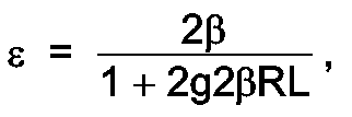


and
- If it is assumed βg′R′<<1, ε<<1, and Isfb≈-J1, then the final short circuit current (Isft) from most positive terminal of head element Rmr to ground is given by

- As a result of the above assumptions, Isft≈J1.
- Acknowledging that parasitic capacitances C′ exist between the bases of the bipolar input transistors (like Q1 and Q2) and ground (Vref) or a substrate, such as a magnetic recording disk, the stored charge is nearly instantaneously discharged during a shorting event from MR element Rmr to the environment. The energy dissipated by the MR element Rmr during such an event is approximated by the expression

where V² is the square of the voltage difference between ground (Vref) and the sum of Vcm and one half the bias current (Iref/2) multiplied by the resistance of MR element Rmr. - The transfer function Vout/Vin has a high-pass frequency characteristic with a -3 dB frequency given by

and a gain in the frequence band of interest of
where - R5
- = R5a + R5b,
- R6
- = R6a + R6b,
- τ1
- = R1C1,
- g2
- = J2/4Vt, and
- re
- = 2Vt/J1.
- The high frequency bandwidth of the circuit may be limited by the inductance of the leads from the MR element Rmr to the input devices together with the low input resistance of the amplifier if the input device transition frequency ft is sufficiently high. The expression for the high frequency bandwidth of the amplifier then becomes

where - Li
- = differential series inductance of leads from MR element to amplifier, and
- Ri
- = sum of the resistances in the input loop of the amplifier
- Fig. 3 plots short circuit current vs. time and depicts the effect of such parasitic capacitance C′. Assume that at time t0 a short occurs. Instead of the value of initial short circuit current indicated by Equations (2) or (3) for either Isib or Isit, which is indicated as A, a larger current due to the parasitic capacitance C′ occurs. Capacitance C′ is to the sum of those parasitic capacitances associated with the base circuit of the input transistors Q1 and Q2. The dashed line A-B indicates what the short circuit profile of the circuit would be without parasitic capacitance. Therefore, the area under the actual short circuit current profile above the dashed line A-B represents the energy approximated in Equation (6); and the total energy dissipated by MR element Rmr is represented by the total area under that profile between the onset and cessation of a short circuit. The short circuit current profile beyond point B is, in the absence of any nonlinear slew rate limitations caused by a the size of capacitor C2 and current Jff3, an exponentially shaped curve with a time constant governed by C2 and its parallel resistance R2 modified by the appropriate gain of what was earlier described as the common mode feedback loop.
- The curve depicted in Fig.3 will increase with time until the final value of short circuit current previously defined in Equation (5) is attained. The time needed from initial to final value of short circuit current is then linearly calculated from the resultant time constant. In the event of slew rate limitation of the common mode feedback loop feedforward current Jff3 and capacitance C2, the time needed from initial to final value of short circuit current is calculated in much the same way as in the above cited U.S. patent 4,879,610, and will be longer than that value which is linearly calculated.
- It will be understood by those skilled in the art that changes in form and detail may be made in the embodiments of amplifier circuit herein described without departing from the scope and teaching of the invention. Accordingly, the low noise amplifier circuit and method herein disclosed are to be considered merely as illustrative, and the invention is to be limited only as specified in the claims.

where rbb′ is the base spreading resistance associated with each input transistor.
Claims (12)
- An amplifier circuit for amplifying an input signal (Vin) generated by a magnetoresistive (MR) element (Rmr) to produce an output signal having a magnitude substantially proportional to dRh/Rh, where Rh is the resistance of the MR element (Rmr) and dRh is the magneto-signal-induced change in the resistance of the MR element (Rmr), the circuit comprising:
an MR element (Rmr);
a current source (J1) coupled to the MR element (Rmr) to produce a bias current in the MR element (Rmr);
characterised in that the circuit further comprises:
first and second interconnected feedback loops,
the first feedback loop for amplifying the input signal (Vin) in the form of deviations from the bias current in such a manner that any DC offset error in the output signal is minimised,
the second feedback loop providing short circuit protection of the MR element (Rmr) by maintaining the MR element (Rmr) at a reference potential to limit current flow through the MR element (Rmr) in the event of a short circuit between the MR element (Rmr) and an adjacent conductive surface. - A circuit as claimed in claim 1 wherein, in use, the feedback loops cooperate to increase the short circuit protection as the bias current decreases and to decrease the short circuit protection as the bias current increases.
- A circuit as claimed in claim 2 comprising an input stage (10) having a pair of bipolar transistors (Q1,Q2), the collectors of the transistors (Q1,Q2) forming output terminals of the input stage (10), the emitters of the transistors (Q1,Q2) being connected to opposite terminals of the MR element (Rmr) for amplifying the input signal, the feedback loops having outputs commonly connected to the bases of the transistors (Q1,Q2).
- A circuit as claimed in claim 3, wherein the first feedback loop is connected to the collectors of the transistors (Q1,Q2) to generate a first control signal in response to any offset potential between the output terminals of the input stage (10), the first control signal being coupled to the bases of the transistors (Q1,Q2) to substantially eliminate any offset potential between the output terminals.
- A circuit as claimed in claim 4 wherein the first control signal is in the form of a differential current signal for adjusting the potential between the bases of the transistors (Q1,Q2) in such a manner that a reference current is divided substantially equally between the transistors (Q1,Q2) to produce the bias current.
- A circuit as claimed in claim 5, wherein the first feedback loop comprises an impendance derived from a resistor (R1) and a capacitor (C1) interposed in parallel between the transistors (Q1,Q2) for defining the frequency response of the circuit in such a manner that the circuit has a dominant zero frequency below a dominant pole frequency to provide a high pass characteristic, the capacitor (C1) serving, to shunt noise generated by the resistor (R1).
- A circuit as claimed in any one of claims 4,5, or 6 comprising:
first circuit means connected to the MR element (Rmr) to detect a centre potential substantially midway between the terminals of the MR element (Rmr), the second feedback loop being configured to generate a second control signal in response to a difference between the sensed centre potential and a predetermined reference potential; and
second circuit means responsive to the second control signal to apply bias signals to the bases of the transistors (Q1,Q2) to maintain the centre potential substantially at the reference potential. - A circuit as claimed in claim 6 wherein the bias signals are substantially equal currents for maintaining the sum of the emitter currents of the transistors (Q1,Q2) substantially equal to a reference current.
- A circuit as claimed in any preceding claim wherein the second feedback loop comprises delay means (R2,C2) for delaying response of the circuit to a short circuit until the short circuit has ceased, the delay means comprising a resistor (R2) and a capacitor (C2) connected in parallel.
- A circuit as claimed in any preceding claim wherein the first and second feedback loops comprise respective differential transconductance amplifiers (g1,g2) for converting an error voltage into a control current output.
- A circuit as claimed in any preceding claim comprising a buffer amplifier (11) for amplifying the circuit output signal and for increasing the bandwidth of the circuit output signal.
- A method of producing electrical output signals whose magnitude is representative of signals produced by a magnetoresistive (MR) element (Rmr) while concurrently protecting the MR element from electrical short circuits between the element and its environment, said method comprising the steps of:
coupling a current source (J1) to one of two terminals of an MR element (Rmr) for producing a bias current through the MR element;
providing an input stage (10) having at least two bipolar transistors (Q1,Q2) and output terminals;
coupling both terminals of said MR element (Rmr) to emitters of said transistors (Q1,Q2) for amplifying current deviations from a time average value of said bias current;
coupling a first feedback circuit means to collectors of said transistors (Q1,Q2) to sense the time average potential between said output terminals to produce a differential control signal, and coupling said differential control signal to bases of said transistors (Q1,Q2) to substantially eliminate the time average offset potential between said output terminals;
coupling other circuit means across both terminals of said MR element (Rmr) for sensing the centre potential of said MR element substantially midway between said both terminals;
using a second feedback circuit means, producing two substantially similar control signals in response to the difference between the sensed centre potential of the MR element (Rmr) and a predetermined reference potential; and
in response to said two similar control signals, applying bias signals to the bases of said transistors (Q1,Q2) to maintain said sensed centre potential substantially at said predetermined reference potential and concurrently insure that substantially no current will flow through any accidental short circuit between any point along said MR element (Rmr) and its said environment.
Applications Claiming Priority (2)
| Application Number | Priority Date | Filing Date | Title |
|---|---|---|---|
| US517093 | 1990-05-01 | ||
| US07/517,093 US5103353A (en) | 1990-05-01 | 1990-05-01 | Low noise amplifier with short circuit protection for signals from magnetoresistive element |
Publications (2)
| Publication Number | Publication Date |
|---|---|
| EP0455472A1 EP0455472A1 (en) | 1991-11-06 |
| EP0455472B1 true EP0455472B1 (en) | 1994-08-10 |
Family
ID=24058329
Family Applications (1)
| Application Number | Title | Priority Date | Filing Date |
|---|---|---|---|
| EP91303921A Expired - Lifetime EP0455472B1 (en) | 1990-05-01 | 1991-05-01 | Low noise amplifier with short circuit protection for signals from magnetoresistive element |
Country Status (4)
| Country | Link |
|---|---|
| US (1) | US5103353A (en) |
| EP (1) | EP0455472B1 (en) |
| JP (1) | JP2574953B2 (en) |
| DE (1) | DE69103321T2 (en) |
Families Citing this family (33)
| Publication number | Priority date | Publication date | Assignee | Title |
|---|---|---|---|---|
| US5122915A (en) * | 1990-09-26 | 1992-06-16 | Minnesota Mining And Manufacturing Company | Low-noise preamplifier for magneto-resistive heads |
| US5204789A (en) * | 1991-01-31 | 1993-04-20 | International Business Machines Corporation | Low noise voltage-biasing amplifier for magnetoresistive element |
| US5323278A (en) * | 1992-09-17 | 1994-06-21 | International Business Machines Corporation | Low noise amplifier circuit for magnetoresistive sensors for fast read-write switching in low supply voltage applications |
| US5309295A (en) * | 1992-10-08 | 1994-05-03 | International Business Machines Corporation | Method and apparatus for biasing a magneto-resistive head |
| MY112702A (en) * | 1992-10-30 | 2001-08-30 | Sony Corp | Reproducing circuit for a magnetic head. |
| US5327303A (en) | 1992-12-18 | 1994-07-05 | Seagate Technology, Inc. | MR preamplifier having feedback loops for minimizing differential low frequency components and regulating common mode low frequency components of the preamplifier output signal |
| KR100309085B1 (en) * | 1993-10-06 | 2001-12-17 | 요트.게.아. 롤페즈 | Devices for reading information from tracks on record carriers |
| US5712739A (en) * | 1993-11-08 | 1998-01-27 | Kabushiki Kaisha Toshiba | Magnetic disk drive system with a composite head unit including a magnetoresistive read only head and an inductive write only head |
| US5444579A (en) * | 1993-12-17 | 1995-08-22 | Imp, Inc. | Preamplifier of a signal from a variable resistance sensor, and a current source |
| US5534818A (en) * | 1993-12-30 | 1996-07-09 | Vtc Inc. | Preamplifier noise filtering circuit |
| US5426542A (en) * | 1994-01-21 | 1995-06-20 | Seagate Technology, Inc. | Electronically coupled high-impedance magnetoresistive preamplifier |
| CA2162515C (en) * | 1994-12-22 | 2000-03-21 | Leonard George Cohen | Jumper tracing system |
| DE69531931T2 (en) * | 1994-12-30 | 2004-07-29 | STMicroelectronics, Inc., Carrollton | Symmetrical ohmic current transformer circuit and method therefor |
| US5770968A (en) * | 1994-12-30 | 1998-06-23 | Sgs-Thomson Microelectronics, Inc. | Differential amplifier with proxy load for control of output common mode range |
| GB2297447A (en) * | 1995-01-27 | 1996-07-31 | Seagate Microelectron Ltd | Amplifier |
| US6341046B1 (en) * | 1995-04-14 | 2002-01-22 | Agere Systems Guardian Corp. | Current biasing voltage sensing preamplifier for magnetoresistive heads |
| US5680280A (en) * | 1995-09-11 | 1997-10-21 | Texas Instruments Incorporated | Magnetic field sensor using heterojunction bipolar transistors |
| US6038090A (en) * | 1996-04-03 | 2000-03-14 | International Business Machines Corporation | Method and apparatus for improving baseline recovery of an MR head using a programmable recovery time constant |
| US5914630A (en) * | 1996-05-10 | 1999-06-22 | Vtc Inc. | MR head preamplifier with output signal amplitude which is independent of head resistance |
| US5834952A (en) * | 1996-10-10 | 1998-11-10 | Vtc Inc. | Open-loop current mode biasing scheme for MR head |
| US5812019A (en) * | 1997-01-10 | 1998-09-22 | Vtc Inc. | Open-loop MR biasing circuit with high power supply and common mode rejection |
| US6134060A (en) * | 1997-06-10 | 2000-10-17 | Stmicroelectronics, Inc. | Current bias, current sense for magneto-resistive preamplifier, preamplifying integrated circuit, and related methods |
| US6005733A (en) * | 1997-06-12 | 1999-12-21 | Vtc, Inc. | Preamplifier bias circuit for use in an AC coupled magnetoresistive read head amplifier |
| US6331921B1 (en) * | 1998-07-06 | 2001-12-18 | Agilent Technologies, Inc | Magneto-resistive head read amplifier |
| JP2000195023A (en) * | 1998-12-25 | 2000-07-14 | Toshiba Corp | Head suspension assembly and magnetic disk drive equipped with same |
| US6252735B1 (en) * | 1999-02-25 | 2001-06-26 | International Business Machines Corporation | Voltage-biasing, voltage-sensing differential preamplifier for magnetoresistive elements |
| US6606212B1 (en) | 1999-03-17 | 2003-08-12 | International Business Machines Corporation | Wideband readout of magneto-resistive heads for data storage |
| US6574061B1 (en) | 1999-08-27 | 2003-06-03 | Seagate Technology Llc | Method and apparatus for run-time temperature compensation of giant magnetoresistive head bias current |
| US7151393B2 (en) * | 2004-11-05 | 2006-12-19 | Guzik Technical Enterprises | High-speed write driver |
| US7667914B2 (en) * | 2006-04-17 | 2010-02-23 | Hitachi Global Storage Technologies Netherlands B.V. | Direct coupled wide-bandwidth front-end with smart bias control amplifier |
| US20130063135A1 (en) * | 2010-05-14 | 2013-03-14 | Hitachi, Ltd. | Magnetic-field-angle measurement device and rotational-angle measurement apparatus using same |
| US8760790B2 (en) * | 2012-03-08 | 2014-06-24 | Lsi Corporation | Analog tunneling current sensors for use with disk drive storage devices |
| CN106093822B (en) * | 2016-07-11 | 2023-02-03 | 深圳市知用电子有限公司 | Automatic zero calibration circuit for differential voltage probe |
Family Cites Families (6)
| Publication number | Priority date | Publication date | Assignee | Title |
|---|---|---|---|---|
| DE3435867A1 (en) * | 1984-09-29 | 1986-04-10 | Bosch Gmbh Robert | DIFFERENTIAL SENSOR |
| US4706138A (en) * | 1986-04-14 | 1987-11-10 | International Business Machines Corporation | Amplification of signals produced by a magnetic sensor |
| US4786993A (en) * | 1986-06-30 | 1988-11-22 | International Business Machines Corporation | Voltage amplifier for constant voltage biasing and amplifying signals from a MR sensor |
| EP0269756B1 (en) * | 1986-08-05 | 1991-01-09 | International Business Machines Corporation | Gain control circuitry for readback apparatus in a recording system using the partial-response, maximum-likelihood technique |
| US4743861A (en) * | 1986-10-27 | 1988-05-10 | International Business Machines Corporation | Frequency response compensation circuit |
| US4879610A (en) * | 1988-09-28 | 1989-11-07 | International Business Machines Corporation | Protective circuit for a magnetoresistive element |
-
1990
- 1990-05-01 US US07/517,093 patent/US5103353A/en not_active Expired - Lifetime
-
1991
- 1991-04-09 JP JP3103459A patent/JP2574953B2/en not_active Expired - Fee Related
- 1991-05-01 DE DE69103321T patent/DE69103321T2/en not_active Expired - Fee Related
- 1991-05-01 EP EP91303921A patent/EP0455472B1/en not_active Expired - Lifetime
Also Published As
| Publication number | Publication date |
|---|---|
| JPH04228101A (en) | 1992-08-18 |
| EP0455472A1 (en) | 1991-11-06 |
| DE69103321D1 (en) | 1994-09-15 |
| DE69103321T2 (en) | 1995-03-23 |
| JP2574953B2 (en) | 1997-01-22 |
| US5103353A (en) | 1992-04-07 |
Similar Documents
| Publication | Publication Date | Title |
|---|---|---|
| EP0455472A1 (en) | Low noise amplifier with short circuit protection for signals from magnetoresistive element | |
| EP0251023B1 (en) | A circuit for biasing a magnetoresistive sensor and amplifying signals produced thereby | |
| EP0361781B1 (en) | Protective circuit for magnetoresistive element | |
| US5204789A (en) | Low noise voltage-biasing amplifier for magnetoresistive element | |
| EP0439299B1 (en) | A circuit for suppressing additive disturbances in data channels | |
| JP2571663B2 (en) | Magnetoresistive head device | |
| EP0009531B1 (en) | Transducer signal amplifier and transducer bias circuits | |
| US4492997A (en) | Reproducing and amplifying circuit for magnetoresistive head | |
| US5345346A (en) | Positive feedback low input capacitance differential amplifier | |
| US5793551A (en) | Amplifier having a differential input capacitance cancellation circuit | |
| US8792198B1 (en) | High impedance low noise cross-coupled amplifier for use in as a preamplifier in a magnetic data storage system | |
| US6650182B2 (en) | Exponential transconductance amplifier | |
| US6710959B1 (en) | Input pole compensation for a disk drive read head | |
| US4743861A (en) | Frequency response compensation circuit | |
| JP2788869B2 (en) | Common emitter type amplifier circuit | |
| US5953173A (en) | High CMRR and sensor-disk short-circuit protection device for dual element magnetoresistive heads | |
| US5717536A (en) | Single-ended cascode amplifier for magnetoresistive sensors | |
| US6211736B1 (en) | Signal amplifying circuit for magnetoresistive element | |
| US6549357B1 (en) | Selectable input pole compensation for a disk drive read head | |
| US20050088203A1 (en) | Tail current generator circuit for bipolar/MOS differential pair to set precise transconductance | |
| US6208482B1 (en) | Signal amplifying circuit for an MR element | |
| US7061321B1 (en) | Low impedance read amplifier for magnetoresistive head | |
| JPS5816206B2 (en) | constant current circuit | |
| JPH01241207A (en) | variable gain amplifier | |
| JPH01238207A (en) | Temperature compensated amplifier circuit |
Legal Events
| Date | Code | Title | Description |
|---|---|---|---|
| PUAI | Public reference made under article 153(3) epc to a published international application that has entered the european phase |
Free format text: ORIGINAL CODE: 0009012 |
|
| AK | Designated contracting states |
Kind code of ref document: A1 Designated state(s): DE FR GB |
|
| 17P | Request for examination filed |
Effective date: 19911219 |
|
| 17Q | First examination report despatched |
Effective date: 19930816 |
|
| GRAA | (expected) grant |
Free format text: ORIGINAL CODE: 0009210 |
|
| AK | Designated contracting states |
Kind code of ref document: B1 Designated state(s): DE FR GB |
|
| REF | Corresponds to: |
Ref document number: 69103321 Country of ref document: DE Date of ref document: 19940915 |
|
| ET | Fr: translation filed | ||
| PLBE | No opposition filed within time limit |
Free format text: ORIGINAL CODE: 0009261 |
|
| STAA | Information on the status of an ep patent application or granted ep patent |
Free format text: STATUS: NO OPPOSITION FILED WITHIN TIME LIMIT |
|
| 26N | No opposition filed | ||
| REG | Reference to a national code |
Ref country code: GB Ref legal event code: IF02 |
|
| REG | Reference to a national code |
Ref country code: FR Ref legal event code: TP |
|
| REG | Reference to a national code |
Ref country code: GB Ref legal event code: 732E |
|
| PGFP | Annual fee paid to national office [announced via postgrant information from national office to epo] |
Ref country code: DE Payment date: 20080606 Year of fee payment: 18 |
|
| PGFP | Annual fee paid to national office [announced via postgrant information from national office to epo] |
Ref country code: GB Payment date: 20080424 Year of fee payment: 18 |
|
| GBPC | Gb: european patent ceased through non-payment of renewal fee |
Effective date: 20090501 |
|
| REG | Reference to a national code |
Ref country code: FR Ref legal event code: ST Effective date: 20100129 |
|
| PG25 | Lapsed in a contracting state [announced via postgrant information from national office to epo] |
Ref country code: FR Free format text: LAPSE BECAUSE OF NON-PAYMENT OF DUE FEES Effective date: 20090602 |
|
| PGFP | Annual fee paid to national office [announced via postgrant information from national office to epo] |
Ref country code: FR Payment date: 20080423 Year of fee payment: 18 |
|
| PG25 | Lapsed in a contracting state [announced via postgrant information from national office to epo] |
Ref country code: GB Free format text: LAPSE BECAUSE OF NON-PAYMENT OF DUE FEES Effective date: 20090501 |
|
| PG25 | Lapsed in a contracting state [announced via postgrant information from national office to epo] |
Ref country code: DE Free format text: LAPSE BECAUSE OF NON-PAYMENT OF DUE FEES Effective date: 20091201 |