EP0455426B1 - Circuit having selectable transfer characteristics - Google Patents
Circuit having selectable transfer characteristics Download PDFInfo
- Publication number
- EP0455426B1 EP0455426B1 EP91303760A EP91303760A EP0455426B1 EP 0455426 B1 EP0455426 B1 EP 0455426B1 EP 91303760 A EP91303760 A EP 91303760A EP 91303760 A EP91303760 A EP 91303760A EP 0455426 B1 EP0455426 B1 EP 0455426B1
- Authority
- EP
- European Patent Office
- Prior art keywords
- circuit means
- values
- signal
- function
- output
- Prior art date
- Legal status (The legal status is an assumption and is not a legal conclusion. Google has not performed a legal analysis and makes no representation as to the accuracy of the status listed.)
- Expired - Lifetime
Links
- 238000012546 transfer Methods 0.000 title claims abstract description 68
- 230000006870 function Effects 0.000 claims abstract description 124
- 238000012545 processing Methods 0.000 claims abstract description 10
- 230000015654 memory Effects 0.000 claims description 31
- 230000001419 dependent effect Effects 0.000 claims 3
- 230000003044 adaptive effect Effects 0.000 abstract description 15
- 238000000034 method Methods 0.000 description 6
- 101150065817 ROM2 gene Proteins 0.000 description 5
- 238000012937 correction Methods 0.000 description 5
- 238000010586 diagram Methods 0.000 description 5
- 101100087530 Caenorhabditis elegans rom-1 gene Proteins 0.000 description 4
- 101001106432 Homo sapiens Rod outer segment membrane protein 1 Proteins 0.000 description 4
- 101100305983 Mus musculus Rom1 gene Proteins 0.000 description 4
- 102100021424 Rod outer segment membrane protein 1 Human genes 0.000 description 4
- 230000000295 complement effect Effects 0.000 description 2
- 238000007476 Maximum Likelihood Methods 0.000 description 1
- 230000008649 adaptation response Effects 0.000 description 1
- 230000005540 biological transmission Effects 0.000 description 1
- 239000002131 composite material Substances 0.000 description 1
- 239000004020 conductor Substances 0.000 description 1
- 230000001934 delay Effects 0.000 description 1
- 230000003111 delayed effect Effects 0.000 description 1
- 230000000694 effects Effects 0.000 description 1
- 230000001747 exhibiting effect Effects 0.000 description 1
- 238000012886 linear function Methods 0.000 description 1
- 230000004044 response Effects 0.000 description 1
- 238000001228 spectrum Methods 0.000 description 1
Images


Classifications
-
- H—ELECTRICITY
- H04—ELECTRIC COMMUNICATION TECHNIQUE
- H04N—PICTORIAL COMMUNICATION, e.g. TELEVISION
- H04N7/00—Television systems
- H04N7/12—Systems in which the television signal is transmitted via one channel or a plurality of parallel channels, the bandwidth of each channel being less than the bandwidth of the television signal
-
- H—ELECTRICITY
- H04—ELECTRIC COMMUNICATION TECHNIQUE
- H04N—PICTORIAL COMMUNICATION, e.g. TELEVISION
- H04N5/00—Details of television systems
- H04N5/14—Picture signal circuitry for video frequency region
- H04N5/20—Circuitry for controlling amplitude response
Definitions
- This invention relates to circuitry of the type which uses memory devices to perform desired transfer functions.
- An example of such circuitry is an adaptive compandor using a memory programmed with a plurality of compansion functions, wherein the signal to be companded is applied as address codes to the memory device.
- US-A-4187519 discloses an apparatus for correcting a video signal.
- An "I-getter” acts as a source of control signals determining, from the input pixels, bias and gain parameters.
- a bias function generator 15 is automatically adjusted by the bias parameters to develop bias correction signals which are applied to the video signal.
- a gain function generator adjusted by the gain parameters develops a gain correction signal which is applied to the video signal.
- Each of the function generators produces correction signals by interpolating from the bias parameters received from the "I-getter". This is a slow process and so a delay element is provided in the video signal path.
- JP-A-59-181876 discloses apparatus for correcting a video signal.
- the apparatus has a plurality of wave form generators storing respective correction waveforms.
- a program stored in a ROM is used to select the appropriate correction waveform.
- the memory device is programmed at respective memory locations with values corresponding to address values transformed by a desired transfer function. For example, if it is desired to scale a digital signal by a particular value, each memory location is programmed with a value equal to the address of the particular memory location multiplied by the scaling value.
- the system may be made adaptive by segmenting the memory device into tables, each of which corresponds to the address values being multiplied by a different scale factor. The particular table utilized at any given time is accessed by appending control bits to the address codes.
- the present inventor realized that for certain families of transfer functions that are implemented in adaptive systems, the memory requirements may be significantly reduced. This is achieved by storing values corresponding to only one representative transfer function in memory. Then by appropriately offsetting the signal applied to the memory and/or scaling the values provided to or by the memory, responses corresponding to others of the family of transfer functions may be effectively realized.
- apparatus for processing a video signal comprising a source of a video input signal; first circuit means having an input terminal and an output terminal, for performing a transfer function on signals delivered to said input terminal; a source of control values; and second circuit means, coupled between said video input signal source and said input terminal of said first circuit means, for performing one of a scaling function and an offset function upon said video input signal; characterized in that said first circuit means comprises a memory means programmed at respective address locations with values representing corresponding address values which have been transformed in accordance with a single predetermined transfer function, and in that the input terminal of said first circuit means corresponds to an address input port of said memory means; whereby said video input signal is subject to a selected one of a family of transfer functions in dependence upon the control value supplied to said second circuit means.
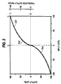
- FIGURE 1 is a graph of a portion of a family of transfer characteristics which can be realized with the present invention.
- FIGURES 2 and 3 are graphs of a single transfer characteristic representative of the family of characteristics illustrated in FIGURE 1 and useful in describing the operation of the invention.
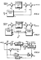
- FIGURES 4, 5 and 8 are block diagrams of alternative embodiments of the invention.
- FIGURES 6 and 7 are block diagrams of alternative compansion systems wherein either the direct compandor or the inverse compandor or both may be realized with circuitry according to the present invention.
- FIGURE 9 is a block diagram of a further embodiment of the invention.
- FIGURES 10 and 11 are block diagrams of alternative adaptive compansion circuits utilizing the circuitry illustrated in FIGURE 9.
- FIGURE 12 is a block diagram of an adaptive peaking circuit embodying the invention.
- Embodiments of the invention are described below in the environment of a compansion system; however its utility is not restricted to this use. It will be appreciated that the invention is applicable to any system requiring selectable transfer functions which transfer functions conform to a family of functions that can be substantially derived from a single representative transfer function.
- FIGURE 1 which graphically illustrates a family of curves representing a plurality of compandor transfer functions.
- Each curve represents a particular input-output relationship which may be employed for particular signal conditions. For example, if it is known that for a particular time interval the input signal is most likely to have values of 50 ⁇ ⁇ ( ⁇ a small value), then the curve labeled TF1 may represent the desired input-output relationship. Alternatively, if for a particular time interval the input signal is expected to have a value of 0+ ⁇ , then the curve labeled TF2 may represent the desired input-output relationship. From the figure it can be seen that the curves have the same general shape as the curve TF1 or a portion of TF1.
- the curve labeled TF3 is similar to curve TF1 but shifted rightward and upward.
- the curve TF4 is similar to curve TF1 but shifted leftward and downward, etc. Note further that if the curve TF4 is translated leftward and downward by 100 units, the combination of curves TF2 and TF4 will have the same general shape as the curve TF1. Finally, assume that the curves shown only represent a small portion of the family of transfer functions desired, i.e., that between curves TF2 and TF4 there are actually a large number of curves.
- the dynamic range of the output values for the family of transfer functions is equal to the dynamic range of possible input values. This is a feature of the exemplary compandor systems described herein below, but is not a requirement of the invention.
- FIGURE 2 which illustrates a transfer function STF representative of the family of transfer functions shown in FIGURE 1.
- the standardized transfer function STF may be derived from the combination of transfer functions TF2 and TF4 connected end-to-end. Note that in FIGURE 2 the input and output dynamic range is twice the input and output dynamic range of the transfer function of FIGURE 1.
- a memory device is programmed to output values indicated by the transfer function STF for the corresponding input levels applied as address codes to its address input port.
- the input signal has a dynamic range of 0 to 100 and that it is desired to realize the transfer function TF1.
- the inflection point of the curve TF1 is at an input level of 50.
- the inflection point of the curve STF is at an input level of zero.
- the input signal is offset by negative 50 units. Offsetting the input signal applied to the memory device by 50 units established the dynamic range of the input levels applied to the memory from -50 to +50 units. This dynamic range of 100 units falls between the dashed lines designated AA.
- the desired output dynamic range is 100 units for the transfer functions shown in FIGURE 1. However, it is seen from FIGURE 2 that the output dynamic range produced by the transfer function STF for the input range between lines AA is approximately 150 units.
- the dynamic range of the output signal may be constrained to 100 units by scaling the output values provided by the memory by the factor 100/150 or 2/3. Scaling the output values constrains the dynamic range to fall between the dashed lines BB in FIGURE 2 and produces the transfer function labeled TF1′.
- the transfer function TF1′ will conform exactly to the function TF1 or very closely approximate the function TF1.
- the output dynamic range of the scaled values is from -50 to +50 units.
- the desired output dynamic range is 0 to 100 units.
- the scaled output values must be offset by a positive 50 units.
- the desired transfer function is TF2.
- the range of input levels applied to the memory is the range between the dashed lines C,C.
- this range is 0 to 100 units, thus no offset is required to be applied to the input signal applied to the memory.
- the output dynamic range defined by the curve STF is 100 units, thus no scaling is required of the output values. In addition no offset is required to be applied to the output values.
- the transfer function TF4 is realized by using that portion of the curve STF to the left of the dashed line C centered on zero units. In this instance the signal input values must be offset by negative 100 units and the signal output values must be offset by positive 100 units. However, no scaling is required of the output values.
- the input offset value IO i is determined by a comparison of the desired function against the representative function. This may be performed graphically or numerically depending upon the shape or symmetry of the functions. Assume that the output value provided by the standard function STF for an input value x is F(x). Assume still further that the input signal range extends from a minimum value x n to a maximum value x x and that the desired output dynamic range for respective ones of the family of functions is OR i .
- the quotient represents the ratio of the desired output dynamic range to the output dynamic range of the function STF for the given input range of values applied to the memory address input.
- Output offsetting may be performed prior to scaling.
- the scale factors G i do not change but the respective values OO i ′ are different.
- the values G i , OO i and IO i are preprogrammed in a second memory which is addressed by a control signal C i at appropriate time intervals. Responsive to the control signals C i , the values G i , OO i and IO i are applied to circuitry coupled in the signal path with the transfer function memory to perform the desired offsetting and scaling functions.
- the required memory for the present system is calculated as follows.
- the total system bit count is 10240 bits or a savings of 514048 bits.
- FIGURE 4 illustrates one embodiment of apparatus for performing the invention.
- the signals are presumed to be parallel-bit pulse code modulated (e.g., PCM binary) signals, and the connections are parallel conductor busses.
- Signal to be processed is applied to an input terminal 10 and control values C i are applied to a control terminal 20.
- the control values may be derived from various sources depending upon the function to be accomplished. For example, if the process function is signal compansion, the control values may represent the signal-to-noise ratio of the input signal and be derived from signal/noise apparatus (not shown). Alternatively, the control values C i may represent predictions of the input signal level and be derived via maximum - likelihood techniques, mean square error techniques or linear prediction methods, etc.
- the input signal is coupled to signal offset circuitry 12 shown as a subtractor.
- Output values from the input offset circuit 12 are applied to the address input port of a read only memory (ROM)14 which is preprogrammed with a transfer function representative of a family of transfer functions.
- the ROM 14 provides output sample values to a scaling circuit 16.
- Scaled samples generated by the scaling circuit 16 are coupled to output offset circuitry 18, shown as an adder.
- Output signal from the output offset circuitry 18 corresponds to the input signal transformed by the desired transfer function.
- the control signal C i is coupled to a control ROM 22 which is preprogrammed with respective offset and scale factor values IO i , OO i and G i , corresponding to respective control signals C i .
- the ROM provides input offset values IO i to the input offset circuitry 12, output offset values OO i to the output offset circuitry 18, and scale factors G i to the scaling circuit 16.
- the offset circuitry 12 and 18 may be realized with either signal addition or subtraction circuits with appropriate choice of the polarity of the offset values programmed in the control ROM22.
- FIGURE 5 illustrates a second embodiment wherein the scaling circuit 32 and the output offset circuitry 30 are coupled in reverse order relative the scaling and offset circuits 16 and 18 in FIGURE 4.
- control ROM is divided into two ROM circuits, control ROM1 and control ROM2.
- One further difference is the application of the sign or polarity bit of the sample provided by the input offset circuitry 12 as an extra address bit to the control ROM2.
- Control ROM1 is programmed with offset values IO i and is responsive to control signals C i .
- Control ROM2 is programmed with offset values OO i ′ and scale factors G i and the system provides the same input-output signal correspondence as the circuitry of FIGURE 4.
- control ROM1 may be eliminated.
- the predicted signal corresponds to the control signal C i , and is applied directly to the subtracter 12 and to the address input of the control ROM 2.
- An example of this type of system is shown in FIGURE 6.
- FIGURE 6 illustrates a differential pulse code modulation (DPCM) system with adaptive compansion circuitry included in the DPCM loop.
- Input signal is applied to a first input terminal of a subtracter 605.
- a predicted video signal is coupled to a second input terminal of subtracter 605, the output of which is coupled to an adaptive compandor 612.
- the predicted video signal is substantially equal to the signal at the same pixel point in the previous image frame.
- the output signal from the subtractor 605 is thus equal to the difference of corresponding pixels in successive frames and nominally will be of small value.
- Output signal from the compandor 612 is coupled to an inverse compandor 620.
- Output signal from the inverse compandor 620 is coupled to an integrator including an adder 640, a scaling circuit 630 and delay elements 650 and 662.
- the delay imposed by the combination of elements 630, 650 and 662 is exactly one frame interval.
- the integrator integrates the signal differences provided by subtracter 605 to reconstruct the video signal in known fashion.
- Integrated signal from the delay element 650 is coupled as the predicted video signal to the subtractor 605.
- the total processing delay imposed by the elements coupled in series between the output and second input terminals of subtracter 605 is substantially one frame interval.
- Delay elements 610, 614 and 616 are included in the system to compensate for delays in generating the control signal for the adaptive compandors 612 and 620.
- the input video signal and the predicted video signal are coupled to a second subtracter 655 which produces output differences equal to the differences generated by the subtracter 605.
- the output signal from subtracter 655 is thus an exact prediction of the input signal applied to the direct compandor 612.
- the direct compandor 612 may be implemented with the circuitry of FIGURE 5, with the control ROM 1 eliminated and the output of subtracter 655 applied directly to subtracter 12 (FIGURE 4) and also as control signal to the address input port of the control ROM 2.
- the circuitry provides DPCM signal at the OUTPUT for transmission or further processing.
- element 612 it may be necessary to filter the control signals applied thereto to preclude the system from becoming unstable and exhibiting limit cycles for example.
- This additional filter is shown as element 615 drawn in phantom.
- FIGURE 6 may be altered as shown in FIGURE 7.
- the FIGURE 5 compandor absent the control ROM1 is used as a direct compandor.
- Companded video signal from the scaling circuit 32 is used as an output signal OUTPUT, and is coupled to an inverse compandor 70 which restores the companded video signal to original form.
- Video signal from the inverse compandor 70 is coupled to a delay circuit 72 and delayed video signal is applied to for example a spatial filter 74.
- Spatial filter 74 in cooperation with the delay element 72, provides an estimate of the input signal. This estimate may be formed as the average of a number of pixels occurring a field or frame earlier and which average correspond to the pixel location represented by the current input signal sample.
- the estimated signal is applied as input offset values IO i to the offset circuitry 12 and also as control values C i to the address input port of the control ROM2.
- control ROM 2 will include two tables, each containing values OO i and G i .
- the use of the sign bit is to modify the transfer function such that when the input signal equals the value IO i , the output signal should equal IO i . In effect the input signal passes through the system unchanged when it is equal to IO i
- the control ROM 2 includes a first table of scale factor values G1 i and output offset values 001 i responsive to the control signals C i and a sign bit signal representing a negative polarity.
- the control ROM 2 includes a second table of scale factor values G2 i and output offset values 002 i responsive to the control values C i and a sign bit signal representing a positive value.
- FIGURE 8 illustrates a system for performing the inverse function of the system of FIGURE 5.
- An inverse function may be realized with a system similar to FIGURE 5 with appropriate programming of the respective memory elements.
- both a direct and inverse function is desired in a single circuit as illustrated in FIGURE 6, it is desirable to minimize hardware.
- the amount of hardware can be minimized if both the direct and inverse functions use common control ROM's.
- Arranging the inverse function circuitry as illustrated in FIGURE 8 permits the use of at least common output offset values OO i and common input offset values IO i for both the direct and inverse function circuits.
- the input signal is applied to a scaling circuit 52 wherein it is scaled by values 1/G i which values are the reciprocals of the values G i stored in the control ROM 1 (FIGURE 5).
- the scaled input signal values are applied to offset circuitry 54 wherein they are offset by values OO i, which values are equal to the output offset values stored in the control ROM 2 (FIGURE 5).
- the values 1/ G i and OO i are provided by a control ROM 60 responsive to control signals C i , which signals C i are equivalent to the control values C i applied to control ROM 1 and control ROM 2 (FIGURE 5).
- the scaled and offset input signal is applied as address codes to a transfer function ROM 56.
- ROM 56 is programmed with the same function STF as the ROM 14 in FIGURE 5, only rotated. That is, considering FIGURE 2, values corresponding to the input levels are programmed at address locations corresponding to respective output levels.
- Output signal samples provided by the transfer function ROM 56 are coupled to an offset circuit 58 wherein the output samples are offset by the values IO i which are equivalent to the input offset values IO i stored in the control ROM 1 (FIGURE 5).
- the values IO i are also provided by the control ROM 60.
- the inverse function system may also be modified to be responsive to a polarity control signal. This is indicated by the auxiliary circuitry including subtracter 61 drawn in phantom.
- FIGURE 9 illustrates another embodiment of the invention which will generate a family of transfer functions from a single transfer function.
- Y(x) x/(1+x 2N ) where x corresponds to the input signal and N is an integer.
- This may be accomplished by scaling the values of x applied to the circuit performing the function Y(x). For example, if the input values x are scaled by the factor 1/ ⁇ , ⁇ a positive value, such that the circuitry performing the function Y(x) operates on the values x/ ⁇ , the values of x defining Xmax and Xmin are ⁇ times the 2N th root of (1/2N-1). Thus the points of occurrence of Xmax and Xmin may be controlled by changing the values of ⁇ . In order to maintain the output dynamic range of the signal Y(x) for the function of equation (10), the values provided by the function circuit may be scaled by the reciprocal of the input scale factor.
- FIGURE 9 is an adaptive function generating circuit of this form.
- FIGURE 9 input samples are applied to a scaling circuit 90 wherein the samples are scaled by a scale factor 1/ ⁇ .
- the scaled samples (x/ ⁇ ) are applied to a functional circuit 91 which may be a ROM programmed with a desired transfer function.
- Transformed samples are coupled to a further scaling circuit 92, wherein the transformed samples are scaled by a scale factor ⁇ .
- the scaling circuit provides the desired output values.
- the scale factor applied thereto may have values different from the reciprocal of the values applied to the scaling circuit 90.
- the scale factor 1/ ⁇ , applied to the scaling circuit 90 is not meant to imply that the values 1/ ⁇ are limited to values less than 1, but may include values greater than 1.
- the scale factors ⁇ and 1/ ⁇ may be provided by a ROM responsive to appropriate control signals, or by other convenient circuitry to promote the desired adaptive response.
- FIGURE 10 illustrates a further embodiment of the invention for providing a plurality of transfer functions using an element (91) arranged to generate a single transfer function.
- circuit elements designated with the same numerals as circuit elements in FIGURE 9 are similar and operate in like fashion.
- Input samples are applied to the minuend input terminal of a subtracter circuit 95, and to the input terminal of the adaptive functional circuitry 96. Output samples from the circuitry 96 are coupled to the subtrahend input terminal of the subtracter 95.
- the point of in flection of the curve is adjustable in accordance with the values 1/ ⁇ and ⁇ applied to the scaling circuits 90 and 92 respectively.
- the scale factor ⁇ is equal to b times ⁇ . (b a variable).
- the value N influences the steepness of the slope at the point of inflection, the larger the value N the greater the slope.
- Equation 15 is useful as an adaptive noise coring circuit wherein the degree of attenuation or coring is determined by the factor ⁇ , and the range of signal over which coring is performed is determined by the factor ⁇ .
- the factors ⁇ and ⁇ may be selected as a function of the signal to noise ratio.
- circuitry of FIGURE 10 may be utilized in a communications receiver to perform a complementary compansion function of signal which has been companded at a transmitter.
- FIGURE 11 illustrates circuitry for performing the complementary function of the circuitry illustrated in FIGURE 10.
- the circuitry of FIGURE 10 tends to compress smaller amplitude signal values and to expand (amplify) larger amplitude signal values, while the circuitry of FIGURE 11 tends to expand smaller amplitude signal values and to compress larger amplitude signal values.
- FIGURE 12 illustrates a further application wherein the invention is used to perform peaking control of a vertical detail signal in a television receiver.
- composite video signal is converted to digital form in an analog-to-digital converter (A/D) and comb filtered to separate the luminance, Y, and chrominance, C, components.
- A/D analog-to-digital converter
- comb filtered chrominance component contains luminance vertical detail which is separated by the bandpass/lowpass filter and added back to the luminance signal in the adder 105, to provide a restored luminance signal.
- the vertical detail signal is also processed by the circuitry 101, 102 and 103 to provide a cored, peaked and pared vertical detail signal which is added to the restored luminance signal in an adder 104 to generate a luminance signal with peaked vertical detail.
- the peaking function is well known, and desirably is arranged to be adjustable so that the user can adjust the displayed image according to his viewing preference.
- the general form of the transfer function applied to the vertical detail signal is illustrated in the block designated 102.
- Elements 101, 102 and 103 are arranged to operate similar to the elements 90, 91 and 92, respectively of FIGURE 9 to permit the user to select one of a family of transfer functions. The user may select the portion of the dynamic range of the vertical detail signal to be peaked by changing the gain factor ⁇ and he may select the degree of peaking by adjusting the gain factor ⁇ .
Abstract
Description
- This invention relates to circuitry of the type which uses memory devices to perform desired transfer functions. An example of such circuitry is an adaptive compandor using a memory programmed with a plurality of compansion functions, wherein the signal to be companded is applied as address codes to the memory device.
- US-A-4187519 discloses an apparatus for correcting a video signal. An "I-getter" acts as a source of control signals determining, from the input pixels, bias and gain parameters. A bias function generator 15 is automatically adjusted by the bias parameters to develop bias correction signals which are applied to the video signal. A gain function generator adjusted by the gain parameters develops a gain correction signal which is applied to the video signal. Each of the function generators produces correction signals by interpolating from the bias parameters received from the "I-getter". This is a slow process and so a delay element is provided in the video signal path.
- JP-A-59-181876 discloses apparatus for correcting a video signal. The apparatus has a plurality of wave form generators storing respective correction waveforms. A program stored in a ROM is used to select the appropriate correction waveform.
- It is known in the art of digital signal processing to use memory devices as functional elements. The memory device is programmed at respective memory locations with values corresponding to address values transformed by a desired transfer function. For example, if it is desired to scale a digital signal by a particular value, each memory location is programmed with a value equal to the address of the particular memory location multiplied by the scaling value. The system may be made adaptive by segmenting the memory device into tables, each of which corresponds to the address values being multiplied by a different scale factor. The particular table utilized at any given time is accessed by appending control bits to the address codes.
- Not all transfer functions can be realized with memory elements in a cost effective manner. Conversely, some transfer functions can only be realized using programmed memories. This is particularly true for certain non-linear functions. Unfortunately the memory devices may become undesirably large. Consider for example an adaptive system processing 8-bit samples, a memory with 8-bit precision, and 8-bit adaptive control signals. The required memory includes 2⁸ tables having 2⁸ memory locations of 8 bits each or a total memory capacity of 524288 bits. A memory of this size will impose appreciable cost to the system.
- The present inventor realized that for certain families of transfer functions that are implemented in adaptive systems, the memory requirements may be significantly reduced. This is achieved by storing values corresponding to only one representative transfer function in memory. Then by appropriately offsetting the signal applied to the memory and/or scaling the values provided to or by the memory, responses corresponding to others of the family of transfer functions may be effectively realized.
- According to the present invention, there is provided apparatus for processing a video signal comprising a source of a video input signal; first circuit means having an input terminal and an output terminal, for performing a transfer function on signals delivered to said input terminal; a source of control values; and second circuit means, coupled between said video input signal source and said input terminal of said first circuit means, for performing one of a scaling function and an offset function upon said video input signal; characterized in that said first circuit means comprises a memory means programmed at respective address locations with values representing corresponding address values which have been transformed in accordance with a single predetermined transfer function, and in that the input terminal of said first circuit means corresponds to an address input port of said memory means; whereby said video input signal is subject to a selected one of a family of transfer functions in dependence upon the control value supplied to said second circuit means.
- FIGURE 1 is a graph of a portion of a family of transfer characteristics which can be realized with the present invention.
- FIGURES 2 and 3 are graphs of a single transfer characteristic representative of the family of characteristics illustrated in FIGURE 1 and useful in describing the operation of the invention.
- FIGURES 4, 5 and 8 are block diagrams of alternative embodiments of the invention.
- FIGURES 6 and 7 are block diagrams of alternative compansion systems wherein either the direct compandor or the inverse compandor or both may be realized with circuitry according to the present invention.
- FIGURE 9 is a block diagram of a further embodiment of the invention.
- FIGURES 10 and 11 are block diagrams of alternative adaptive compansion circuits utilizing the circuitry illustrated in FIGURE 9.
- FIGURE 12 is a block diagram of an adaptive peaking circuit embodying the invention.
- Embodiments of the invention are described below in the environment of a compansion system; however its utility is not restricted to this use. It will be appreciated that the invention is applicable to any system requiring selectable transfer functions which transfer functions conform to a family of functions that can be substantially derived from a single representative transfer function.
- Refer to FIGURE 1 which graphically illustrates a family of curves representing a plurality of compandor transfer functions. Each curve represents a particular input-output relationship which may be employed for particular signal conditions. For example, if it is known that for a particular time interval the input signal is most likely to have values of 50± Δ (Δ a small value), then the curve labeled TF1 may represent the desired input-output relationship. Alternatively, if for a particular time interval the input signal is expected to have a value of 0+Δ, then the curve labeled TF2 may represent the desired input-output relationship. From the figure it can be seen that the curves have the same general shape as the curve TF1 or a portion of TF1. The curve labeled TF3 is similar to curve TF1 but shifted rightward and upward. The curve TF4 is similar to curve TF1 but shifted leftward and downward, etc. Note further that if the curve TF4 is translated leftward and downward by 100 units, the combination of curves TF2 and TF4 will have the same general shape as the curve TF1. Finally, assume that the curves shown only represent a small portion of the family of transfer functions desired, i.e., that between curves TF2 and TF4 there are actually a large number of curves.
- The dynamic range of the output values for the family of transfer functions is equal to the dynamic range of possible input values. This is a feature of the exemplary compandor systems described herein below, but is not a requirement of the invention.
- Refer to FIGURE 2 which illustrates a transfer function STF representative of the family of transfer functions shown in FIGURE 1. In this example the standardized transfer function STF may be derived from the combination of transfer functions TF2 and TF4 connected end-to-end. Note that in FIGURE 2 the input and output dynamic range is twice the input and output dynamic range of the transfer function of FIGURE 1.
- Assume a memory device is programmed to output values indicated by the transfer function STF for the corresponding input levels applied as address codes to its address input port. Assume further that the input signal has a dynamic range of 0 to 100 and that it is desired to realize the transfer function TF1.
- The inflection point of the curve TF1 is at an input level of 50. The inflection point of the curve STF is at an input level of zero. To apply the transfer function at the inflection point of the curve STF to the input signal level of 50, the input signal is offset by negative 50 units. Offsetting the input signal applied to the memory device by 50 units established the dynamic range of the input levels applied to the memory from -50 to +50 units. This dynamic range of 100 units falls between the dashed lines designated AA. The desired output dynamic range is 100 units for the transfer functions shown in FIGURE 1. However, it is seen from FIGURE 2 that the output dynamic range produced by the transfer function STF for the input range between lines AA is approximately 150 units. The dynamic range of the output signal may be constrained to 100 units by scaling the output values provided by the memory by the
factor 100/150 or 2/3. Scaling the output values constrains the dynamic range to fall between the dashed lines BB in FIGURE 2 and produces the transfer function labeled TF1′. Depending upon the method of generating the curve STF, relative to the conformity of the family of transfer functions to a single curve, the transfer function TF1′ will conform exactly to the function TF1 or very closely approximate the function TF1. - There is one further requirement to render the scaled output values (TF1′) in conformance with the transfer function TF1. The output dynamic range of the scaled values is from -50 to +50 units. The desired output dynamic range is 0 to 100 units. Thus the scaled output values must be offset by a positive 50 units.
- Refer to FIGURE 3 and assume that the desired transfer function is TF2. Assuming that the inflection point of the curve TF2 is at zero units, and that the inflection point of the curve STF is at 0 units, the range of input levels applied to the memory is the range between the dashed lines C,C. For both FIGURE 1 and FIGURE 2 this range is 0 to 100 units, thus no offset is required to be applied to the input signal applied to the memory. Between the dashed lines C,C, the output dynamic range defined by the curve STF is 100 units, thus no scaling is required of the output values. In addition no offset is required to be applied to the output values.
- The transfer function TF4 is realized by using that portion of the curve STF to the left of the dashed line C centered on zero units. In this instance the signal input values must be offset by negative 100 units and the signal output values must be offset by positive 100 units. However, no scaling is required of the output values.
- Assume that all of the transfer functions of the desired family and the representative function are monotonic. The input offset value IOi is determined by a comparison of the desired function against the representative function. This may be performed graphically or numerically depending upon the shape or symmetry of the functions. Assume that the output value provided by the standard function STF for an input value x is F(x). Assume still further that the input signal range extends from a minimum value xn to a maximum value xx and that the desired output dynamic range for respective ones of the family of functions is ORi. The scale factor Gi for the particular selected function is determined from the relation

where F(xx - IOi) and F(xn - IOi) correspond to the maximum and minimum values provided in accordance with the function STF for the offset input range. The quotient represents the ratio of the desired output dynamic range to the output dynamic range of the function STF for the given input range of values applied to the memory address input. - The output offset value OOi is determined as follows for a system where scaling precedes the application of the output offset value. Let Fi(xn) equal the maximum output level for the respective desired transfer function. Then it is desired that


- Output offsetting may be performed prior to scaling. In this instance the scale factors Gi, do not change but the respective values OOi′ are different. The values OOi` are determined from the relation

or
- The values Gi, OOi and IOi are preprogrammed in a second memory which is addressed by a control signal Ci at appropriate time intervals. Responsive to the control signals Ci, the values Gi, OOi and IOi are applied to circuitry coupled in the signal path with the transfer function memory to perform the desired offsetting and scaling functions.
- Considering 8-bit input samples, 8-bit output samples and 2⁸ different transfer functions, the required memory for the present system is calculated as follows. The memory for storing the standard function has 2⁹ x 8 = 4096 bits (note the STF memory has twice the input dynamic range). Each of the 2⁸ transfer functions requires three values (Gi, OOi and IOi) which are assumed to be 8-bits, for a total of 8x3x2⁸ = 6144 bits. The total system bit count is 10240 bits or a savings of 514048 bits.
- FIGURE 4 illustrates one embodiment of apparatus for performing the invention. In the figure the signals are presumed to be parallel-bit pulse code modulated (e.g., PCM binary) signals, and the connections are parallel conductor busses. Signal to be processed is applied to an
input terminal 10 and control values Ci are applied to acontrol terminal 20. The control values may be derived from various sources depending upon the function to be accomplished. For example, if the process function is signal compansion, the control values may represent the signal-to-noise ratio of the input signal and be derived from signal/noise apparatus (not shown). Alternatively, the control values Ci may represent predictions of the input signal level and be derived via maximum - likelihood techniques, mean square error techniques or linear prediction methods, etc. The input signal is coupled to signal offsetcircuitry 12 shown as a subtractor. Output values from the input offsetcircuit 12 are applied to the address input port of a read only memory (ROM)14 which is preprogrammed with a transfer function representative of a family of transfer functions. TheROM 14 provides output sample values to ascaling circuit 16. Scaled samples generated by the scalingcircuit 16 are coupled to output offsetcircuitry 18, shown as an adder. Output signal from the output offsetcircuitry 18 corresponds to the input signal transformed by the desired transfer function. - The control signal Ci is coupled to a
control ROM 22 which is preprogrammed with respective offset and scale factor values IOi, OOi and Gi, corresponding to respective control signals Ci. The ROM provides input offset values IOi to the input offsetcircuitry 12, output offset values OOi to the output offsetcircuitry 18, and scale factors Gi to thescaling circuit 16. Note that the offsetcircuitry - FIGURE 5 illustrates a second embodiment wherein the scaling
circuit 32 and the output offsetcircuitry 30 are coupled in reverse order relative the scaling and offsetcircuits circuitry 12 as an extra address bit to the control ROM2. - Consider first that the sign bit is not connected to control ROM2. Control ROM1 is programmed with offset values IOi and is responsive to control signals Ci. Control ROM2 is programmed with offset values OOi′ and scale factors Gi and the system provides the same input-output signal correspondence as the circuitry of FIGURE 4.
- Next consider that it is possible to predict the instantaneous value of the input signal and that there is a different transfer function for each input signal value. In this instance the control ROM1 may be eliminated. The predicted signal corresponds to the control signal Ci, and is applied directly to the
subtracter 12 and to the address input of the control ROM 2. An example of this type of system is shown in FIGURE 6. - FIGURE 6 illustrates a differential pulse code modulation (DPCM) system with adaptive compansion circuitry included in the DPCM loop. Input signal is applied to a first input terminal of a subtracter 605. A predicted video signal is coupled to a second input terminal of subtracter 605, the output of which is coupled to an
adaptive compandor 612. The predicted video signal is substantially equal to the signal at the same pixel point in the previous image frame. The output signal from the subtractor 605 is thus equal to the difference of corresponding pixels in successive frames and nominally will be of small value. Output signal from thecompandor 612 is coupled to aninverse compandor 620. Output signal from theinverse compandor 620 is coupled to an integrator including anadder 640, ascaling circuit 630 and delayelements elements delay element 650 is coupled as the predicted video signal to the subtractor 605. The total processing delay imposed by the elements coupled in series between the output and second input terminals of subtracter 605 is substantially one frame interval. Delayelements adaptive compandors - The input video signal and the predicted video signal are coupled to a
second subtracter 655 which produces output differences equal to the differences generated by the subtracter 605. The output signal fromsubtracter 655 is thus an exact prediction of the input signal applied to thedirect compandor 612. Thus thedirect compandor 612 may be implemented with the circuitry of FIGURE 5, with thecontrol ROM 1 eliminated and the output ofsubtracter 655 applied directly to subtracter 12 (FIGURE 4) and also as control signal to the address input port of the control ROM 2. As illustrated in FIGURE 6 the circuitry provides DPCM signal at the OUTPUT for transmission or further processing. - Depending on the transfer functions implemented by
element 612 it may be necessary to filter the control signals applied thereto to preclude the system from becoming unstable and exhibiting limit cycles for example. This additional filter is shown aselement 615 drawn in phantom. - Alternatively, if it is desired to provide companded video signal as output signal rather than a companded DPCM signal, the system of FIGURE 6 may be altered as shown in FIGURE 7. The FIGURE 5 compandor absent the control ROM1 is used as a direct compandor. Companded video signal from the scaling
circuit 32 is used as an output signal OUTPUT, and is coupled to aninverse compandor 70 which restores the companded video signal to original form. Video signal from theinverse compandor 70 is coupled to adelay circuit 72 and delayed video signal is applied to for example aspatial filter 74.Spatial filter 74 in cooperation with thedelay element 72, provides an estimate of the input signal. This estimate may be formed as the average of a number of pixels occurring a field or frame earlier and which average correspond to the pixel location represented by the current input signal sample. - The estimated signal is applied as input offset values IOi to the offset
circuitry 12 and also as control values Ci to the address input port of the control ROM2. - Referring back to FIGURE 5 the system will be described with the inclusion of the sign bit from
subtracter 12. In this instance the control ROM 2 will include two tables, each containing values OOi and Gi. The use of the sign bit is to modify the transfer function such that when the input signal equals the value IOi, the output signal should equal IOi. In effect the input signal passes through the system unchanged when it is equal to IOi The control ROM 2 includes a first table of scale factor values G1i and output offset values 001i responsive to the control signals Ci and a sign bit signal representing a negative polarity. The values G1i and OO1i are given by

In addition the control ROM 2 includes a second table of scale factor values G2i and output offset values 002i responsive to the control values Ci and a sign bit signal representing a positive value. The values G2i and 002i are given by

where xx is the upper limit of the dynamic range of the input signal. - FIGURE 8 illustrates a system for performing the inverse function of the system of FIGURE 5. An inverse function may be realized with a system similar to FIGURE 5 with appropriate programming of the respective memory elements. However if both a direct and inverse function is desired in a single circuit as illustrated in FIGURE 6, it is desirable to minimize hardware. The amount of hardware can be minimized if both the direct and inverse functions use common control ROM's. Arranging the inverse function circuitry as illustrated in FIGURE 8 permits the use of at least common output offset values OOi and common input offset values IOi for both the direct and inverse function circuits.
- In FIGURE 8 the input signal is applied to a
scaling circuit 52 wherein it is scaled byvalues 1/Gi which values are the reciprocals of the values Gi stored in the control ROM 1 (FIGURE 5). The scaled input signal values are applied to offsetcircuitry 54 wherein they are offset by values OOi, which values are equal to the output offset values stored in the control ROM 2 (FIGURE 5). Thevalues 1/ Gi and OOi are provided by acontrol ROM 60 responsive to control signals Ci, which signals Ci are equivalent to the control values Ci applied to controlROM 1 and control ROM 2 (FIGURE 5). - The scaled and offset input signal is applied as address codes to a
transfer function ROM 56.ROM 56 is programmed with the same function STF as theROM 14 in FIGURE 5, only rotated. That is, considering FIGURE 2, values corresponding to the input levels are programmed at address locations corresponding to respective output levels. - Output signal samples provided by the
transfer function ROM 56 are coupled to an offsetcircuit 58 wherein the output samples are offset by the values IOi which are equivalent to the input offset values IOi stored in the control ROM 1 (FIGURE 5). The values IOi are also provided by thecontrol ROM 60. - The inverse function system may also be modified to be responsive to a polarity control signal. This is indicated by the auxiliary
circuitry including subtracter 61 drawn in phantom. - FIGURE 9 illustrates another embodiment of the invention which will generate a family of transfer functions from a single transfer function. Consider, for example, the function Y(x) given by

where x corresponds to the input signal and N is an integer. Y(x) is skew symmetric about zero, has a value of zero at x=0, tends toward zero for values of x greater than Xmax and less than Xmin and wherein Xmax and Xmin are equal to plus and minus the 2Nth root of 1/(2N-1) respectively. Consider also that it is desired to adaptively control the values of x defining Xmax and Xmin. This may be accomplished by scaling the values of x applied to the circuit performing the function Y(x). For example, if the input values x are scaled by thefactor 1/α,α a positive value, such that the circuitry performing the function Y(x) operates on the values x/α, the values of x defining Xmax and Xmin are α times the 2Nth root of (1/2N-1). Thus the points of occurrence of Xmax and Xmin may be controlled by changing the values of α. In order to maintain the output dynamic range of the signal Y(x) for the function of equation (10), the values provided by the function circuit may be scaled by the reciprocal of the input scale factor. FIGURE 9 is an adaptive function generating circuit of this form. - In FIGURE 9 input samples are applied to a
scaling circuit 90 wherein the samples are scaled by ascale factor 1/α. The scaled samples (x/α) are applied to afunctional circuit 91 which may be a ROM programmed with a desired transfer function. Transformed samples are coupled to afurther scaling circuit 92, wherein the transformed samples are scaled by a scale factor α. The scaling circuit provides the desired output values. Assuming that the transfer function performed by thecircuitry 91 corresponds to the function defined byequation 10, the scaling circuit provides output samples of the form given by
or more generally
Note however that for some applications it may not be necessary to include thelatter scaling circuit 92. In addition, if scalingcircuit 92 is included, the scale factor applied thereto may have values different from the reciprocal of the values applied to thescaling circuit 90. Further, thescale factor 1/α, applied to thescaling circuit 90 is not meant to imply that thevalues 1/α are limited to values less than 1, but may include values greater than 1. The scale factors α and 1/α may be provided by a ROM responsive to appropriate control signals, or by other convenient circuitry to promote the desired adaptive response. - FIGURE 10 illustrates a further embodiment of the invention for providing a plurality of transfer functions using an element (91) arranged to generate a single transfer function. In FIGURE 10 (and FIGURE 11) circuit elements designated with the same numerals as circuit elements in FIGURE 9 are similar and operate in like fashion.
- Input samples are applied to the minuend input terminal of a
subtracter circuit 95, and to the input terminal of the adaptivefunctional circuitry 96. Output samples from thecircuitry 96 are coupled to the subtrahend input terminal of thesubtracter 95. Thesubtracter 95 provides output samples, OUTPUT in conformance with the function
Assume that thefunctional element 91 performs the function defined byequation 10 and that the scale factor β is equal to α. In this instance the output signal is equal to
This function is similar to the function TF1 illustrated in FIGURE 1, except that for larger values of the input signal the slope of the curve tends toward 1. The point of in flection of the curve is adjustable in accordance with thevalues 1/α and α applied to the scalingcircuits subtracter 95 is given by
This arrangement permits establishment of the slope of the curve at x = 0 to the value (1-b). Note the value N influences the steepness of the slope at the point of inflection, the larger the value N the greater the slope. - The function defined by equation 15 is useful as an adaptive noise coring circuit wherein the degree of attenuation or coring is determined by the factor β, and the range of signal over which coring is performed is determined by the factor α. The factors α and β may be selected as a function of the signal to noise ratio.
- The functions defined by either equations (14) or (15) are also useful for performing adaptive compansion, similar to the function performed by the circuitry of FIGURE 8. That is the circuitry of FIGURE 10 may be utilized in a communications receiver to perform a complementary compansion function of signal which has been companded at a transmitter.
- FIGURE 11 illustrates circuitry for performing the complementary function of the circuitry illustrated in FIGURE 10. The circuitry of FIGURE 10 tends to compress smaller amplitude signal values and to expand (amplify) larger amplitude signal values, while the circuitry of FIGURE 11 tends to expand smaller amplitude signal values and to compress larger amplitude signal values.
- FIGURE 12 illustrates a further application wherein the invention is used to perform peaking control of a vertical detail signal in a television receiver. In FIGURE 12 composite video signal is converted to digital form in an analog-to-digital converter (A/D) and comb filtered to separate the luminance, Y, and chrominance, C, components. The lower frequency spectrum of the comb filtered chrominance component contains luminance vertical detail which is separated by the bandpass/lowpass filter and added back to the luminance signal in the
adder 105, to provide a restored luminance signal. The vertical detail signal is also processed by thecircuitry adder 104 to generate a luminance signal with peaked vertical detail. The peaking function is well known, and desirably is arranged to be adjustable so that the user can adjust the displayed image according to his viewing preference. The general form of the transfer function applied to the vertical detail signal is illustrated in the block designated 102.Elements elements
Claims (4)
- Apparatus for processing a video signal comprising:
a source (10) of a video input signal;
first circuit means (14) having an input terminal and an output terminal, for performing a transfer function on signals delivered to said input terminal;
a source (22) of control values; and
second circuit means (12), coupled between said video input signal source and said input terminal of said first circuit means, for performing one of a scaling function and an offset function upon said video input signal;
characterized in that said first circuit means comprises a memory means (ROM 14) programmed at respective address locations with values representing corresponding address values which have been transformed in accordance with a single predetermined transfer function, and in that the input terminal of said first circuit means corresponds to an address input port of said memory means;
whereby said video input signal is subject to a selected one of a family of transfer functions in dependence upon the control value supplied to said second circuit means. - Processing apparatus in accordance with claim 1, further characterized by third circuit means (16) responsive to the signal output of said first circuit means, and to an additional control value from said source of control values, for performing one of a scaling function and an offset function upon the signal output of said first circuit means;
whereby the selection of said one of said family of transfer functions to which said video input signal is subject is additionally dependent upon the additional control value supplied to said third circuit means. - Processing apparatus in accordance with claim 1 or claim 2, further characterized by further circuit means (54), serially coupled with said second circuit means (52) between said video input signal source and said input terminal of said first circuit means, and also responsive to a further control value from said source of control values, for performing one of a scaling function and an offset function different from the one of said scaling and offset functions performed by said second circuit means (52);
whereby the selection of said one of said family of transfer functions to which said video input signal is subject is additionally dependent upon the further control value supplied to said further circuit means (54). - Processing apparatus in accordance with claim 1 or claim 2, further characterized by additional circuit means (32), serially coupled with said third circuit means (30), and also responsive to another control value from said source of control values, for performing one of a scaling function and an offset function different from the one of said scaling and offset functions performed by said third circuit means (30);
whereby the selection of said one of said family of transfer functions to which said video input signal is subject is also dependent upon said another control value supplied to said additional circuit means (32).
Applications Claiming Priority (4)
| Application Number | Priority Date | Filing Date | Title |
|---|---|---|---|
| US51834690A | 1990-05-03 | 1990-05-03 | |
| US630606 | 1990-12-20 | ||
| US07/630,606 US5258928A (en) | 1990-05-03 | 1990-12-20 | Parts efficient memory based functional circuit having selectable transfer characteristics |
| US518346 | 1995-08-23 |
Publications (3)
| Publication Number | Publication Date |
|---|---|
| EP0455426A2 EP0455426A2 (en) | 1991-11-06 |
| EP0455426A3 EP0455426A3 (en) | 1992-03-11 |
| EP0455426B1 true EP0455426B1 (en) | 1995-12-06 |
Family
ID=27059421
Family Applications (1)
| Application Number | Title | Priority Date | Filing Date |
|---|---|---|---|
| EP91303760A Expired - Lifetime EP0455426B1 (en) | 1990-05-03 | 1991-04-25 | Circuit having selectable transfer characteristics |
Country Status (13)
| Country | Link |
|---|---|
| US (1) | US5258928A (en) |
| EP (1) | EP0455426B1 (en) |
| JP (1) | JP3208711B2 (en) |
| KR (1) | KR100227245B1 (en) |
| CN (1) | CN1030028C (en) |
| AT (1) | ATE131329T1 (en) |
| CA (1) | CA2040760C (en) |
| DE (1) | DE69115111T2 (en) |
| ES (1) | ES2080896T3 (en) |
| FI (1) | FI912127A (en) |
| MY (1) | MY112550A (en) |
| PT (1) | PT97557B (en) |
| TR (1) | TR26793A (en) |
Families Citing this family (9)
| Publication number | Priority date | Publication date | Assignee | Title |
|---|---|---|---|---|
| JP2924079B2 (en) * | 1990-05-14 | 1999-07-26 | ソニー株式会社 | Gamma correction circuit |
| US5357278A (en) * | 1993-01-14 | 1994-10-18 | Sony Electronics, Inc. | Integrated linear/non-linear static and controllable dynamic companding |
| US6285710B1 (en) | 1993-10-13 | 2001-09-04 | Thomson Licensing S.A. | Noise estimation and reduction apparatus for video signal processing |
| BE1007777A3 (en) * | 1993-11-23 | 1995-10-17 | Philips Electronics Nv | Non-linear signal. |
| US9020998B2 (en) | 2008-10-14 | 2015-04-28 | Dolby Laboratories Licensing Corporation | Efficient computation of driving signals for devices with non-linear response curves |
| CA2816367C (en) * | 2010-11-02 | 2018-02-20 | I-CES (Innovative Compression Engineering Solutions) | Method for compressing digital values of image, audio and/or video files. |
| US10244245B2 (en) * | 2015-06-08 | 2019-03-26 | Qualcomm Incorporated | Content-adaptive application of fixed transfer function to high dynamic range (HDR) and/or wide color gamut (WCG) video data |
| JP7186374B2 (en) | 2017-10-04 | 2022-12-09 | パナソニックIpマネジメント株式会社 | VIDEO SIGNAL PROCESSING DEVICE, VIDEO DISPLAY SYSTEM, AND VIDEO SIGNAL PROCESSING METHOD |
| WO2019069753A1 (en) * | 2017-10-04 | 2019-04-11 | パナソニックIpマネジメント株式会社 | Video signal processing device, video display system, and video signal processing method |
Family Cites Families (17)
| Publication number | Priority date | Publication date | Assignee | Title |
|---|---|---|---|---|
| US4212072A (en) * | 1978-03-07 | 1980-07-08 | Hughes Aircraft Company | Digital scan converter with programmable transfer function |
| US4187519A (en) * | 1978-08-17 | 1980-02-05 | Rockwell International Corporation | System for expanding the video contrast of an image |
| IL58119A (en) * | 1979-08-27 | 1983-03-31 | Yeda Res & Dev | Histogram image enhancement system |
| JPS5661873A (en) * | 1979-10-25 | 1981-05-27 | Sony Corp | Digital video signal processor |
| NL190093C (en) * | 1979-12-17 | 1993-10-18 | Victor Company Of Japan | COMPRESSING AND EXPANDING SYSTEM. |
| US4335427A (en) * | 1980-04-21 | 1982-06-15 | Technicare Corporation | Method of selecting a preferred difference image |
| US4445138A (en) * | 1981-12-21 | 1984-04-24 | Hughes Aircraft Company | Real time dynamic range compression for image enhancement |
| US4435792A (en) * | 1982-06-30 | 1984-03-06 | Sun Microsystems, Inc. | Raster memory manipulation apparatus |
| US4516167A (en) * | 1982-11-30 | 1985-05-07 | Rca Corporation | Compression of the dynamic range of video signals |
| US4518994A (en) * | 1982-12-20 | 1985-05-21 | Rca Corporation | Communication system compandor |
| JPS59163953A (en) * | 1983-03-08 | 1984-09-17 | Canon Inc | Picture processing device |
| JPS59181876A (en) * | 1983-03-31 | 1984-10-16 | Toshiba Corp | Device for correcting video signal |
| US4575749A (en) * | 1983-07-28 | 1986-03-11 | Rca Corporation | Component companding in a multiplexed component system |
| US4621290A (en) * | 1984-04-12 | 1986-11-04 | Rca Corporation | Piecewise linear digital signal processor as for digital video vertical detail processing |
| US4771192A (en) * | 1986-11-14 | 1988-09-13 | The Grass Valley Group, Inc. | Digital clip and gain circuit |
| GB2203012B (en) * | 1987-03-30 | 1991-02-20 | Sony Corp | Differential pulse code modulation |
| JP2521183Y2 (en) * | 1987-09-29 | 1996-12-25 | ソニー株式会社 | Digital signal processing circuit |
-
1990
- 1990-12-20 US US07/630,606 patent/US5258928A/en not_active Expired - Lifetime
-
1991
- 1991-04-18 CA CA002040760A patent/CA2040760C/en not_active Expired - Fee Related
- 1991-04-24 MY MYPI91000696A patent/MY112550A/en unknown
- 1991-04-25 ES ES91303760T patent/ES2080896T3/en not_active Expired - Lifetime
- 1991-04-25 EP EP91303760A patent/EP0455426B1/en not_active Expired - Lifetime
- 1991-04-25 DE DE69115111T patent/DE69115111T2/en not_active Expired - Fee Related
- 1991-04-25 AT AT91303760T patent/ATE131329T1/en not_active IP Right Cessation
- 1991-04-26 KR KR1019910006748A patent/KR100227245B1/en not_active IP Right Cessation
- 1991-04-30 CN CN91102989A patent/CN1030028C/en not_active Expired - Fee Related
- 1991-05-02 FI FI912127A patent/FI912127A/en unknown
- 1991-05-02 JP JP19468091A patent/JP3208711B2/en not_active Expired - Fee Related
- 1991-05-03 TR TR00432/91A patent/TR26793A/en unknown
- 1991-05-03 PT PT97557A patent/PT97557B/en not_active IP Right Cessation
Also Published As
| Publication number | Publication date |
|---|---|
| JP3208711B2 (en) | 2001-09-17 |
| CA2040760C (en) | 1998-06-30 |
| DE69115111T2 (en) | 1996-07-11 |
| KR910021155A (en) | 1991-12-20 |
| FI912127A (en) | 1991-11-04 |
| CA2040760A1 (en) | 1991-11-04 |
| JPH05346803A (en) | 1993-12-27 |
| CN1030028C (en) | 1995-10-11 |
| DE69115111D1 (en) | 1996-01-18 |
| TR26793A (en) | 1994-08-08 |
| MY112550A (en) | 2001-07-31 |
| PT97557B (en) | 1998-11-30 |
| EP0455426A2 (en) | 1991-11-06 |
| CN1056204A (en) | 1991-11-13 |
| US5258928A (en) | 1993-11-02 |
| KR100227245B1 (en) | 1999-11-01 |
| ES2080896T3 (en) | 1996-02-16 |
| FI912127A0 (en) | 1991-05-02 |
| PT97557A (en) | 1993-05-31 |
| ATE131329T1 (en) | 1995-12-15 |
| EP0455426A3 (en) | 1992-03-11 |
Similar Documents
| Publication | Publication Date | Title |
|---|---|---|
| US6097848A (en) | Noise reduction apparatus for electronic edge enhancement | |
| US5473373A (en) | Digital gamma correction system for low, medium and high intensity video signals, with linear and non-linear correction | |
| KR920008630B1 (en) | Compensation circuit of horizontal corner | |
| JP2549753B2 (en) | Gamma correction circuit and method | |
| JPH07143358A (en) | Dynamic gamma contrast control method and circuit | |
| KR970068620A (en) | Image quality improvement method using quantized mean separation histogram equalization and its circuit | |
| US4355304A (en) | Digital compandor | |
| US5132796A (en) | Method and apparatus for digitally processing gamma pedestal and gain | |
| EP0455426B1 (en) | Circuit having selectable transfer characteristics | |
| KR20020025868A (en) | Video-apparatus with histogram modification means | |
| CA2085754C (en) | Gradation compensation apparatus of video image | |
| JPH0418865A (en) | Gamma correction circuit | |
| US5179528A (en) | Signal processing system and method implementing a non-linear transfer function approximated by a piecewise linear transformation | |
| EP0098016A2 (en) | A method of and a circuit arrangement for producing a gamma corrected video signal | |
| JPH05314165A (en) | Pseudo movement averaging circuit | |
| US5233410A (en) | Interpolating digital signal clipping circuit and composite video clipping circuit utilizing same | |
| EP0514196A2 (en) | Picture quality improving appartus for compensating contour of images | |
| US5739871A (en) | Automatic high-luminance compression method and circuit adopting the same | |
| CA1177174A (en) | Cascaded roms for signal processing | |
| US5214510A (en) | Adaptive digital aperture compensation and noise cancel circuit | |
| JPH1091779A (en) | Digital x-ray image processor | |
| JPH0218789B2 (en) | ||
| US7027098B2 (en) | Picture-signal processing apparatus and method using weighting for black-level control | |
| JPS6346881A (en) | Digital outline correcting circuit | |
| JP3722740B2 (en) | Video processing apparatus and video processing method |
Legal Events
| Date | Code | Title | Description |
|---|---|---|---|
| PUAI | Public reference made under article 153(3) epc to a published international application that has entered the european phase |
Free format text: ORIGINAL CODE: 0009012 |
|
| AK | Designated contracting states |
Kind code of ref document: A2 Designated state(s): AT BE CH DE DK ES FR GB GR IT LI LU NL SE |
|
| PUAL | Search report despatched |
Free format text: ORIGINAL CODE: 0009013 |
|
| AK | Designated contracting states |
Kind code of ref document: A3 Designated state(s): AT BE CH DE DK ES FR GB GR IT LI LU NL SE |
|
| RAP1 | Party data changed (applicant data changed or rights of an application transferred) |
Owner name: RCA THOMSON LICENSING CORPORATION |
|
| 17P | Request for examination filed |
Effective date: 19920824 |
|
| 17Q | First examination report despatched |
Effective date: 19940628 |
|
| GRAA | (expected) grant |
Free format text: ORIGINAL CODE: 0009210 |
|
| AK | Designated contracting states |
Kind code of ref document: B1 Designated state(s): AT DE ES FR GB IT NL |
|
| REF | Corresponds to: |
Ref document number: 131329 Country of ref document: AT Date of ref document: 19951215 Kind code of ref document: T |
|
| REF | Corresponds to: |
Ref document number: 69115111 Country of ref document: DE Date of ref document: 19960118 |
|
| ET | Fr: translation filed | ||
| REG | Reference to a national code |
Ref country code: ES Ref legal event code: FG2A Ref document number: 2080896 Country of ref document: ES Kind code of ref document: T3 |
|
| ITF | It: translation for a ep patent filed |
Owner name: ING. C. GREGORJ S.P.A. |
|
| PLBE | No opposition filed within time limit |
Free format text: ORIGINAL CODE: 0009261 |
|
| STAA | Information on the status of an ep patent application or granted ep patent |
Free format text: STATUS: NO OPPOSITION FILED WITHIN TIME LIMIT |
|
| 26N | No opposition filed | ||
| PGFP | Annual fee paid to national office [announced via postgrant information from national office to epo] |
Ref country code: AT Payment date: 19980305 Year of fee payment: 8 |
|
| PGFP | Annual fee paid to national office [announced via postgrant information from national office to epo] |
Ref country code: NL Payment date: 19980430 Year of fee payment: 8 |
|
| PG25 | Lapsed in a contracting state [announced via postgrant information from national office to epo] |
Ref country code: AT Free format text: LAPSE BECAUSE OF NON-PAYMENT OF DUE FEES Effective date: 19990425 |
|
| PG25 | Lapsed in a contracting state [announced via postgrant information from national office to epo] |
Ref country code: NL Free format text: LAPSE BECAUSE OF NON-PAYMENT OF DUE FEES Effective date: 19991101 |
|
| NLV4 | Nl: lapsed or anulled due to non-payment of the annual fee |
Effective date: 19991101 |
|
| REG | Reference to a national code |
Ref country code: GB Ref legal event code: 732E |
|
| REG | Reference to a national code |
Ref country code: GB Ref legal event code: IF02 |
|
| REG | Reference to a national code |
Ref country code: FR Ref legal event code: D6 |
|
| REG | Reference to a national code |
Ref country code: GB Ref legal event code: 746 Effective date: 20030228 |
|
| PGFP | Annual fee paid to national office [announced via postgrant information from national office to epo] |
Ref country code: FR Payment date: 20070424 Year of fee payment: 17 |
|
| PGFP | Annual fee paid to national office [announced via postgrant information from national office to epo] |
Ref country code: GB Payment date: 20080326 Year of fee payment: 18 |
|
| PGFP | Annual fee paid to national office [announced via postgrant information from national office to epo] |
Ref country code: ES Payment date: 20080520 Year of fee payment: 18 Ref country code: DE Payment date: 20080422 Year of fee payment: 18 |
|
| PGFP | Annual fee paid to national office [announced via postgrant information from national office to epo] |
Ref country code: IT Payment date: 20080428 Year of fee payment: 18 |
|
| REG | Reference to a national code |
Ref country code: FR Ref legal event code: ST Effective date: 20081231 |
|
| PG25 | Lapsed in a contracting state [announced via postgrant information from national office to epo] |
Ref country code: FR Free format text: LAPSE BECAUSE OF NON-PAYMENT OF DUE FEES Effective date: 20080430 |
|
| GBPC | Gb: european patent ceased through non-payment of renewal fee |
Effective date: 20090425 |
|
| PG25 | Lapsed in a contracting state [announced via postgrant information from national office to epo] |
Ref country code: DE Free format text: LAPSE BECAUSE OF NON-PAYMENT OF DUE FEES Effective date: 20091103 |
|
| PG25 | Lapsed in a contracting state [announced via postgrant information from national office to epo] |
Ref country code: GB Free format text: LAPSE BECAUSE OF NON-PAYMENT OF DUE FEES Effective date: 20090425 |
|
| REG | Reference to a national code |
Ref country code: ES Ref legal event code: FD2A Effective date: 20090427 |
|
| PG25 | Lapsed in a contracting state [announced via postgrant information from national office to epo] |
Ref country code: ES Free format text: LAPSE BECAUSE OF NON-PAYMENT OF DUE FEES Effective date: 20090427 |
|
| PG25 | Lapsed in a contracting state [announced via postgrant information from national office to epo] |
Ref country code: IT Free format text: LAPSE BECAUSE OF NON-PAYMENT OF DUE FEES Effective date: 20090425 |