EP0454417B1 - Image signal processing apparatus - Google Patents
Image signal processing apparatus Download PDFInfo
- Publication number
- EP0454417B1 EP0454417B1 EP91303645A EP91303645A EP0454417B1 EP 0454417 B1 EP0454417 B1 EP 0454417B1 EP 91303645 A EP91303645 A EP 91303645A EP 91303645 A EP91303645 A EP 91303645A EP 0454417 B1 EP0454417 B1 EP 0454417B1
- Authority
- EP
- European Patent Office
- Prior art keywords
- level
- value
- representative
- image signal
- amplification
- Prior art date
- Legal status (The legal status is an assumption and is not a legal conclusion. Google has not performed a legal analysis and makes no representation as to the accuracy of the status listed.)
- Expired - Lifetime
Links
Images


Classifications
-
- H—ELECTRICITY
- H04—ELECTRIC COMMUNICATION TECHNIQUE
- H04N—PICTORIAL COMMUNICATION, e.g. TELEVISION
- H04N5/00—Details of television systems
- H04N5/44—Receiver circuitry for the reception of television signals according to analogue transmission standards
- H04N5/57—Control of contrast or brightness
-
- H—ELECTRICITY
- H04—ELECTRIC COMMUNICATION TECHNIQUE
- H04N—PICTORIAL COMMUNICATION, e.g. TELEVISION
- H04N9/00—Details of colour television systems
- H04N9/64—Circuits for processing colour signals
- H04N9/68—Circuits for processing colour signals for controlling the amplitude of colour signals, e.g. automatic chroma control circuits
Definitions
- the present invention relates to image signal processing apparatus which provides processing to image signals in order to adjust the image contrast in the display of pictures corresponding to image signals.
- the magnitude of a gain to the said image signal has been regulated, for example, irrespective of changes in the level of an input image signal. Therefore, once the contrast level is set, a specified gain is provided whether the level of the input image signal is high or low.
- Fig. 1 shows the basic structure to conduct the above conventional contrast adjustment.
- the input image signal A is amplified at the amplifier 1 according to the gain adjusted by the contrast control knob 2, i.e., the contrast level to be given as output image signal B.
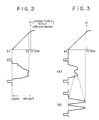
- Fig. 2 there exists such relationship as shown in Fig. 2 between the electric current (IK) of the cathode and the voltage (EGK) between the grid and the cathode of the braun tube (CRT) which is generally used to display pictures corresponding to image signals. Also, there is proportional relationship between the cathode current and brightness.
- the Ec in the Figure indicates a cut-off voltage, below which there is no glow of cathode current on the braun tube. Es is also the maximum permissible driving voltage, above which the cathode current becomes too large and the spot diameter of electron beam grows large resulting in the inability to show minute part of a picture and increase of X ray generated from the braun tube.
- the voltage applied to the braun tube should fall between Ec and Es.
- the range from Ec to Es is the dynamic range of the braun tube, which determines the contrast ratio of the braun tube (the ratio from black to white).
- the braun tube should be operated with the amplitude of image signal within this range in order to gain pictures having sufficient contrast.
- the image signals do not always move over the entire span of this range.
- the signal is located at a spot close to the black level indicated on (a) of Fig. 3, namely a small level of an image signal.
- the variable part of the signal as shown in (b) of Fig. 3, should be amplified and operated.
- a commercially variable method to utilize effectively the actuation range of the braun tube has been developed in which an autopedestal (Fig. 4) is given to lower automatically the level of pictoral signal corresponding to the most black part of the picture down to the pedestral level or the gain of the amplifier for image signals is raised (as in Fig. 3(b)) to utilize the full actuation range of the braun tube.
- This invention intends to provide an image signal processing apparatus and a method which solve the above-mentioned problems as set out in claims 1 and 10.
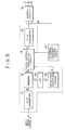
- Fig. 5 is a drawing showing an outlined structure of the contrast adjustment circuit as the first embodiments of the present invention.
- item 11 is an A/D converter
- item 12 is a field or frame memory
- item 13 is low-pass filter
- item 14 is a detection operation circuit
- item 15 is a gain control operation circuit
- item 16 is a D/A converter
- item 17 is an external contrast control circuit.
- the input image signal A is converted to the digital data B at the A/D converter 11.
- the digital data B is supplied to the digital data of the memory 12, in which the digital data corresponding to one screen (1 field or 1 frame volume) is stored.
- the digital data stored in the said memory is supplied to LPF13.
- the data, after the over-shoot and pre-shoot generated in the pictorial signal indicated on the digital data by said LPF3 are removed, are supplied to the detection/operation circuit 14.
- the detection and operation circuit 14 and the gain control circuit 15 have the structure shown in Fig. 6.
- the digital data output by the above LPF13 are supplied to the detection/operation unit 20 which is arranged to calculate the average value of the digital data corresponding to one screen (APL) accumulated in the above memory 12 using the supplied digital data and also detect the maximum value (WP) and the minimum value (DP) of the digital data corresponding to one screen which are stored in the above memory 12.
- the detection/operation part 20 determines the gain value of pictorial signal based on the following operation formula from the detected or operated avarage value (APL), the maximum value (WP), the minimum value (DP) and the threshold maximum value (W) and the threshold minimum value (D) of the image signal.
- APL detected or operated avarage value
- WP maximum value
- DP minimum value
- W threshold maximum value
- D threshold minimum value
- the above operation formula (1) is the formula to determine the gain value G1 in case the digital data value is larger than the average value (APL).
- the operation formula (2) is the formula to determine the gain value G2 is the formula to determine the gain value G2 in case the digital data value is smaller than the average value (APL).
- the gain values G1 and G2 are equal to or greater than 1.
- the calculated average value APL is supplied to the judgement part 26 within the gain control operation circuit 15 which will be explained later.
- the gain values G1 and G2 are supplied to the judgement part 21 within the detection/operation circuit 14.
- the judgement part 21 outputs a signal to select one of the gain adjustment parts 22, 23 and 24 which generate differing gain adjustment data according to the size of the gain values G1 and G2 supplied from the above detection/operation part 20.
- the judgement part 21 supplies the above selection signal to the gain adjustment part 22 and supplies, for example, the gain adjustment GA which indicates "O" from the gain adjustment part 22 to the judgment amplification part 25. If 1.2 ⁇ G1 and G2 ⁇ 3, the above selection signal is supplied to the gain adjustment part 23, the gain adjustment data GB which, for example, indicates "1.5” is supplied from the said gain adjustment part 23 to the judgment amplification part 25. Further, in case 3 ⁇ G1 and G3, the above selection signal is supplied to the gain adjustment part 24, and the gain adjustment data GC which, for example, indicates "3" is supplied from the gain adjustment part 24 to the judgement amplification part 25.
- Values for the gain adjustment data GA, GB and GC which are output from the gain adjustment parts 22, 23 and 24 can be set by the external contrast control circuit 17.
- the average value data APL output from the above-mentioned detection/operation part 20 is supplied also to the judgment part within the gain control operation circuit 15 as stated above.
- the judgement part 26 determines whether the digital data stored in the above memory 12 is larger or smaller than the said average value data APL and supplies the results to the judgment amplification part 25.
- the judgement amplification part 25 sets the amplification gain of judgement data supplied from the above judgement part 26 and of the digital data supplied from the above memory 12 according to the gain adjustment data GA, GB and GC supplied from the above gain adjustment parts 22, 23 and 24. And the said digital data are amplified according to the set amplification gain and the amplified digital data G is supplied to the D/A converter 16 of Fig. 5.
- the digital data supplied from the gain control operation circuit 15 are converted to the analogue image signal (luminance signal Y). Then, the luminance signal Y is output from the said D/A converter 16 and supplied to the matrix circuit 18 along with the color differential signals I and Q processed in a color signal processing circuit which is not shown on the drawing.
- the matrix circuit 18 forms RGB signals from the supplied luminance signal Y, color differential signals I and Q, which are then supplied to the display part, including the braun tube, which is not shown on the drawing.
- Fig. 7 shows the amplification processing of the above image signals according to the distribution condition of levels of input image signals.
- Fig. 7A shows the case in which the image signal shows ordinary brightness
- Fig. 7B is the case of dark situation
- Fig. 7C is the case of bright situation.
- the left-hand side shows the distribution condition of the level of input image signals
- the right-hand side indicates the distribution condition of the level of image signals after the amplification processing.
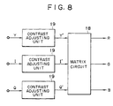
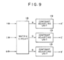
- contrast adjustment is made only about the luminance signal of image signals.
- the contrast adjustment part 19 having the same structure as in Fig. 5 is provided not only to the luminance signal Y but also to color differential signals I and Q to do the same processing, thereby conducting contrast adjustment most suitable for color picture receiving tube.
- the level control is given to the luminance signal Y, color differential signals I and Q for the purpose of contrast adjustment.
- matrix processing is done to the luminance signal Y and color differential signals I and Q, and after being converted to RGB signal, the contrast adjustment part 19 may be provided to each of the R (red), G (green) and B (blue) signals to make contrast adjustment.
- the dynamic range of the LC driving circuit is so narrow that the contrast adjustment by the structure shown in the embodiment is particularly effective, making it possible to restrict the phenomena of white collapse and black collapse leading to the display of contrast picture which is easy to see.
- Fig. 10 shows an outlined structure of the contrast adjustment circuit as the second embodiment of the present invention.
- the item 31 is an input terminal through which image signal is fed.
- the item 32 is an analogue/digital (A/D) converter is which after going through the low-pass filter (not shown on the drawing) to restrict the band in a specified area, the analogue image signal is subjected to sampling and quantizing and then converted into the digital data.
- the item 33 is a memory which memorizes and delays the digital data formed on the above A/D converter 32.
- Item 34 is a image processing circuit to do such processing as the multiplying of digital data by a coefficient.
- Item 35 is a digital/analogue (D/A) converter.
- Item 36 is a detection/operation circuit which detects the maximum value and the minimum value and calculate an intermediate value between the detected maximum value and minimum values.
- Item 37 is a coefficient calculation circuit to determine the amplification rate.
- Item 38 is a coefficient operation circuit which multiplies the coefficient calculated from item 37, a coefficient calculation circuit by the coefficient generated at item 39, a coefficient generation circuit.
- Item 39 is a coefficient generation circuit which generates a coefficient varying the amplification rate to obtain a desired contrast ratio.
- Item 40 is a control part which variably controls coefficients generated from item 39, the above coefficient generation circuit.
- the image signal input from the input terminal 31 is band-restricted through the low-pass filter (not shown on the drawing), which restricts bands in a desired band, and is then subjected to sampling (not shown on the drawing since the sampling clock generation circuit and power source are known) and quantizing at the A/D converter 32.
- the signals are converted into digital data, supplied to the memory circuit 33 one after another. For example, after data corresponding to one period of horizontal scanning are memorized, the signals are sent to the image processing circuit 34.
- the digital data output from the A/D converter 32 are supplied to the detection/operation circuit 36.
- the detection operation circuit 36 detects, from among digital data expressing effective image signals excluding synchronous part and pedestal part of image signals shown on Fig. 11, the maximum level data as the maximum value Da, the minimum level data as the minimum value Db, and the intermediate value Dc as [minimum value + ( the maximum value - the minimun value 2 ) ] to supply data to the coefficient calculation circuit 37.
- a detection operation circuit as Da With the maximum value obtained in the item 36, a detection operation circuit as Da, the minimum value as Db, the intermediate value as Dc, the maximum value of the possible digital data as F, the pedestal level as G and further Da - Db 2 as Dd the coefficient calculation curcuit 37 selects and outputs the smaller of F - Dc Dd and Dc - G Dd .
- this coefficient calculation circuit 37 is capable of obtaining the intermediate value of the image signals and then calculating the largest possible amplification rate without clipping the image signals.
- the coefficient generation circuit 39 generates a coefficient with which an operator varies the image contrast freely as desired. Thus, according to the indication data generated at the control part 40, a coefficient below is generated. If the coefficient value is 1, the contrast ratio is improved.
- the coefficient calculated at the coefficient calculation circuit 3 can extend from the minimum value of 1 to the maximum value close to infinity.
- the coefficient generated from the coefficient generation circuit 39 is below 1.
- the coefficient is input to the coefficient operation circuit 38 to conduct the multiplication processing.
- the coefficient operation circuit 38 determines (or do limiter) the maximum value of the amplification rate (coefficient) which is to be set. For example, if the maximum value of the amplification rate (coefficient) is 2, the signal in Fig. 12A does not become a signal of Fig. 12B but is comparable to that of Fig. 12C, not leading to visual uncomfortableness.
- the coefficient value generated from the coefficient generation circuit 39 the coefficient calculated in the coefficient operation circuit 38 is more than 1 and lower than 2, then being supplied to the image processing circuit 34.
- the intermediate value obtained by the detection/operation circuit 36 is multiplied by the coefficient (amplification rate) obtained in the coefficient operation circuit 38 to conduct digital data processing as shown in Fig. 11B.
- the digital data processed in the image processing circuit are converted to analogue signals at the D/A converter 35 and, after being subjected to the band restriction in the low-pass filter shown on the drawing, are supplied to the driving circuit of the braun tube shown on the drawing.
- the maximum value and the minimum value of image signals are detected by digitalizing the image signals. Further, by obtaining the intermediate value and structuring to vary the gain coefficient of image signals according to the said intermediate value, the picture corresponding to the image signal can be displayed with sufficient contrast with substantially improved quality of picture.
- the contrast is improved by moving the intermediate value Dc.
- the moving amount of the intermediate value Dc in this case should be 15 - 20 % so that there may be no sense of incongruity visually.
- the contrast is improved as shown in Fig. 13B by shifting the level of intermediate value or doing white elongation or black elongation with respect to signals which have a small contrast ratio at a place close to white peak or black level.
- the term "average” above encompasses not only the arithmetic mean, but also any other measure giving a representative signal value (for example, the median value, or the geometric mean, or the sum).
- the average may be derived from the output of the low pass filter 13, and hence represent the low pass filtered average.
- the low pass filter 13 may, for example, be arranged to smooth out sudden peak white or peak black pixel values due to, for example, noise.
- the average may alternatively be derived to omit such isolated peak values from the calculation of the average.
Landscapes
- Engineering & Computer Science (AREA)
- Multimedia (AREA)
- Signal Processing (AREA)
- Television Receiver Circuits (AREA)
- Controls And Circuits For Display Device (AREA)
- Picture Signal Circuits (AREA)
Description
- The present invention relates to image signal processing apparatus which provides processing to image signals in order to adjust the image contrast in the display of pictures corresponding to image signals.
- Traditionally, when the contrast of pictures is adjusted in the display of pictures corresponding to image signals, the magnitude of a gain to the said image signal has been regulated, for example, irrespective of changes in the level of an input image signal. Therefore, once the contrast level is set, a specified gain is provided whether the level of the input image signal is high or low.
- One such technique is disclosed in EP-A-0 204 593.
- Fig. 1 shows the basic structure to conduct the above conventional contrast adjustment.
- In Fig. 1, the input image signal A is amplified at the
amplifier 1 according to the gain adjusted by thecontrast control knob 2, i.e., the contrast level to be given as output image signal B. - Incidentally, in the case of gain adjustment by the conventional method of contrast control, since the image signals are amplified at a specified gain irrespective of the amplitude of the image signal, there occurs such degradation as white saturation and black crush on the braun tube screen which displays pictures corresponding to the image signals. As a result, the optimum range of contrast becomes very narrow, leading to changes in brightness or incoming light to the braun tube or inability to display good pictures unless the contrast is re-adjusted each time the input image signals change.
- On the other hand, there exists such relationship as shown in Fig. 2 between the electric current (IK) of the cathode and the voltage (EGK) between the grid and the cathode of the braun tube (CRT) which is generally used to display pictures corresponding to image signals. Also, there is proportional relationship between the cathode current and brightness. The Ec in the Figure indicates a cut-off voltage, below which there is no glow of cathode current on the braun tube. Es is also the maximum permissible driving voltage, above which the cathode current becomes too large and the spot diameter of electron beam grows large resulting in the inability to show minute part of a picture and increase of X ray generated from the braun tube.
- For this reason, the voltage applied to the braun tube should fall between Ec and Es. In other words, the range from Ec to Es is the dynamic range of the braun tube, which determines the contrast ratio of the braun tube (the ratio from black to white).
- To put it another way, the braun tube should be operated with the amplitude of image signal within this range in order to gain pictures having sufficient contrast.
- However, the image signals do not always move over the entire span of this range. Sometimes, the signal is located at a spot close to the black level indicated on (a) of Fig. 3, namely a small level of an image signal. In order to increase the contrast by utilizing the dynamic range of the braun tube, the variable part of the signal, as shown in (b) of Fig. 3, should be amplified and operated. Based on such basic thought a commercially variable method to utilize effectively the actuation range of the braun tube has been developed in which an autopedestal (Fig. 4) is given to lower automatically the level of pictoral signal corresponding to the most black part of the picture down to the pedestral level or the gain of the amplifier for image signals is raised (as in Fig. 3(b)) to utilize the full actuation range of the braun tube.
- But if the autopedestal is done in the above example of the conventional method on such picture which is bright and uniform like a single color of white, sufficient brightness is not gained since the color tends to be drawn to the direction of black. At the same time, the amplitude ratio becomes too large giving uncomfortable picture or if the gain of the amplifier is increased, the standard image signal gives higher contrast than the conventional one but entails such drawbacks as EGK exceeding ES from time to time in the case of image signals which contain white peaks. To prevent this, a limiter is sometimes given. However, since the white peak is limited by the limiter, there is a shortcoming that the while peak (white color) is not sufficient.
- This invention intends to provide an image signal processing apparatus and a method which solve the above-mentioned problems as set out in
claims - Other objectives and characteristics of the present invention will become evident from the detailed explanation about the mode of working with reference to the drawings which follow.
-
- Fig. 1 is a drawing showing the basic structure to make the conventional contrast adjustment;
- Fig. 2 is a drawing showing the characteristics of the braun tube;
- Fig. 3 is a drawing to explain the contrast of a picture;
- Fig. 4 is a drawing to explain the actuation of autopedestal;
- Fig. 5 is a drawing showing an outlined structure of a contrast adjustment circuit as the first embodiment of the present invention;
- Fig. 6 is a drawing showing the structure of the detection/operation circuit and the gain control circuit in the contrast adjustment circuit shown in the above Fig. 5;
- Figs. 7A-7C are drawings to explain the contrast adjustment actuation by the contrast adjustment circuit shown in the above Fig. 5;
- Figs. 8 and 9 are drawings showing the structure of application examples in the embodiment indicated in the above Fig. 5;
- Fig. 10 is a drawing showing an outlined structure of the contrast adjustment circuit as the second embodiment of the present invention;
- Figs. 11A and 11B are drawings to explain the maximum, minimum and intermediate values used in the second embodiment of the present invention;
- Figs. 12A-12C are drawings to explain the amplitude ratio used in the second embodiment of the present invention;
- Figs. 13A and 13B are drawings to explain the procedure for movement of intermediate value used in the third embodiment of the present invention.
- Below explained is the present invention with reference to its embodiments.
- Fig. 5 is a drawing showing an outlined structure of the contrast adjustment circuit as the first embodiments of the present invention.
- In Fig. 5, item 11 is an A/D converter,
item 12 is a field or frame memory,item 13 is low-pass filter,item 14 is a detection operation circuit,item 15 is a gain control operation circuit,item 16 is a D/A converter, anditem 17 is an external contrast control circuit. - In Fig. 5, the input image signal A is converted to the digital data B at the A/D converter 11. Then, the digital data B is supplied to the digital data of the
memory 12, in which the digital data corresponding to one screen (1 field or 1 frame volume) is stored. The digital data stored in the said memory is supplied to LPF13. Then, the data, after the over-shoot and pre-shoot generated in the pictorial signal indicated on the digital data by said LPF3 are removed, are supplied to the detection/operation circuit 14. - The detection and
operation circuit 14 and thegain control circuit 15 have the structure shown in Fig. 6. - As shown in Fig.6, the digital data output by the above LPF13 are supplied to the detection/
operation unit 20 which is arranged to calculate the average value of the digital data corresponding to one screen (APL) accumulated in theabove memory 12 using the supplied digital data and also detect the maximum value (WP) and the minimum value (DP) of the digital data corresponding to one screen which are stored in theabove memory 12. - The detection/
operation part 20 determines the gain value of pictorial signal based on the following operation formula from the detected or operated avarage value (APL), the maximum value (WP), the minimum value (DP) and the threshold maximum value (W) and the threshold minimum value (D) of the image signal.

- The above operation formula (1) is the formula to determine the gain value G1 in case the digital data value is larger than the average value (APL). The operation formula (2) is the formula to determine the gain value G2 is the formula to determine the gain value G2 in case the digital data value is smaller than the average value (APL). In the operation formulae (1) and (2), the gain values G1 and G2 are equal to or greater than 1.
- As mentioned above, in the detection/
operation part 20, the calculated average value APL is supplied to thejudgement part 26 within the gaincontrol operation circuit 15 which will be explained later. The gain values G1 and G2 are supplied to thejudgement part 21 within the detection/operation circuit 14. - The
judgement part 21 outputs a signal to select one of thegain adjustment parts operation part 20. - In other words, in case the gain values G1 and G2 supplied from the detection/
operation part 20 are, for example, 1≤G1 and G2 < 1.2, thejudgement part 21 supplies the above selection signal to thegain adjustment part 22 and supplies, for example, the gain adjustment GA which indicates "O" from thegain adjustment part 22 to thejudgment amplification part 25. If 1.2 < G1 and G2 < 3, the above selection signal is supplied to thegain adjustment part 23, the gain adjustment data GB which, for example, indicates "1.5" is supplied from the saidgain adjustment part 23 to thejudgment amplification part 25. Further, in case 3 ≤ G1 and G3, the above selection signal is supplied to thegain adjustment part 24, and the gain adjustment data GC which, for example, indicates "3" is supplied from thegain adjustment part 24 to thejudgement amplification part 25. - Values for the gain adjustment data GA, GB and GC which are output from the
gain adjustment parts contrast control circuit 17. - The average value data APL output from the above-mentioned detection/
operation part 20 is supplied also to the judgment part within the gaincontrol operation circuit 15 as stated above. Thejudgement part 26 determines whether the digital data stored in theabove memory 12 is larger or smaller than the said average value data APL and supplies the results to thejudgment amplification part 25. - The
judgement amplification part 25 sets the amplification gain of judgement data supplied from theabove judgement part 26 and of the digital data supplied from theabove memory 12 according to the gain adjustment data GA, GB and GC supplied from the abovegain adjustment parts A converter 16 of Fig. 5. - In the D/
A converter 16, the digital data supplied from the gaincontrol operation circuit 15 are converted to the analogue image signal (luminance signal Y). Then, the luminance signal Y is output from the said D/A converter 16 and supplied to thematrix circuit 18 along with the color differential signals I and Q processed in a color signal processing circuit which is not shown on the drawing. Thematrix circuit 18 forms RGB signals from the supplied luminance signal Y, color differential signals I and Q, which are then supplied to the display part, including the braun tube, which is not shown on the drawing. - Fig. 7 shows the amplification processing of the above image signals according to the distribution condition of levels of input image signals. Fig. 7A shows the case in which the image signal shows ordinary brightness, Fig. 7B is the case of dark situation and Fig. 7C is the case of bright situation. In the Fig. 7, the left-hand side shows the distribution condition of the level of input image signals and the right-hand side indicates the distribution condition of the level of image signals after the amplification processing.
- As shown in Fig. 7, according to the embodiment of the present invention, no black collapse nor white collapse occur even in case the level distribution of the input image signals is situated close to the threshold dynamic range of image signal level, and the dynamic range of the image signal level (the area of W through D in Fig. 7) is utilized effectively to make the most suitable adjustment of contrast, leading to the display of the appealing picture.
- In the embodiment of Fig. 5, contrast adjustment is made only about the luminance signal of image signals. As shown in Fig. 8, the
contrast adjustment part 19 having the same structure as in Fig. 5 is provided not only to the luminance signal Y but also to color differential signals I and Q to do the same processing, thereby conducting contrast adjustment most suitable for color picture receiving tube. In the embodiment indicated on Figs. 5 and 8, the level control is given to the luminance signal Y, color differential signals I and Q for the purpose of contrast adjustment. As shown in Fig. 9, matrix processing is done to the luminance signal Y and color differential signals I and Q, and after being converted to RGB signal, thecontrast adjustment part 19 may be provided to each of the R (red), G (green) and B (blue) signals to make contrast adjustment. - In this way, according to the structure of this embodiment, automatic adjustment of contrast becomes possible depending upon the level of--the input image signals so that the phenomena of white collapse and black collapse on the screen of the display equipment can be inhibited even when image signals of large levels are input, leading to the display of appropriate contrast picture, which is easy to see.
- In case the display equipment has the braun tube, it becomes possible to prevent tailing phenomenon due to the storage phenomenon of CRT drive transistor which-is easy to take place when pictorial signals of high level are input, resulting in the improvement of picture quality.
- Furthermore, in case the display equipment has liquid crystal display, the dynamic range of the LC driving circuit is so narrow that the contrast adjustment by the structure shown in the embodiment is particularly effective, making it possible to restrict the phenomena of white collapse and black collapse leading to the display of contrast picture which is easy to see.
- What follows below is an explanation about the second and third embodiments of the present invention.
- Fig. 10 shows an outlined structure of the contrast adjustment circuit as the second embodiment of the present invention. The
item 31 is an input terminal through which image signal is fed. Theitem 32 is an analogue/digital (A/D) converter is which after going through the low-pass filter (not shown on the drawing) to restrict the band in a specified area, the analogue image signal is subjected to sampling and quantizing and then converted into the digital data. Theitem 33 is a memory which memorizes and delays the digital data formed on the above A/D converter 32.Item 34 is a image processing circuit to do such processing as the multiplying of digital data by a coefficient.Item 35 is a digital/analogue (D/A) converter.Item 36 is a detection/operation circuit which detects the maximum value and the minimum value and calculate an intermediate value between the detected maximum value and minimum values.Item 37 is a coefficient calculation circuit to determine the amplification rate.Item 38 is a coefficient operation circuit which multiplies the coefficient calculated fromitem 37, a coefficient calculation circuit by the coefficient generated atitem 39, a coefficient generation circuit.Item 39 is a coefficient generation circuit which generates a coefficient varying the amplification rate to obtain a desired contrast ratio.Item 40 is a control part which variably controls coefficients generated fromitem 39, the above coefficient generation circuit. - In the above structure, the image signal input from the
input terminal 31 is band-restricted through the low-pass filter (not shown on the drawing), which restricts bands in a desired band, and is then subjected to sampling (not shown on the drawing since the sampling clock generation circuit and power source are known) and quantizing at the A/D converter 32. Thus, the signals are converted into digital data, supplied to thememory circuit 33 one after another. For example, after data corresponding to one period of horizontal scanning are memorized, the signals are sent to theimage processing circuit 34. - The digital data output from the A/
D converter 32 are supplied to the detection/operation circuit 36. Thedetection operation circuit 36 detects, from among digital data expressing effective image signals excluding synchronous part and pedestal part of image signals shown on Fig. 11, the maximum level data as the maximum value Da, the minimum level data as the minimum value Db, and the intermediate value Dc as
coefficient calculation circuit 37. With the maximum value obtained in theitem 36, a detection operation circuit as Da, the minimum value as Db, the intermediate value as Dc, the maximum value of the possible digital data as F, the pedestal level as G and further


- By obtaining difference between the maximum possible value of the digital data or the pedestal level and the intermediate level with the above-mentioned operation, it can be determined which of the maximum value direction and the pedestal level direction has smaller allowance for amplification. Then, division by Dd is made to obtain the amplification rate. In other words, this
coefficient calculation circuit 37 is capable of obtaining the intermediate value of the image signals and then calculating the largest possible amplification rate without clipping the image signals. - The
coefficient generation circuit 39 generates a coefficient with which an operator varies the image contrast freely as desired. Thus, according to the indication data generated at thecontrol part 40, a coefficient below is generated. If the coefficient value is 1, the contrast ratio is improved. - The coefficient calculated at the coefficient calculation circuit 3 can extend from the minimum value of 1 to the maximum value close to infinity. The coefficient generated from the
coefficient generation circuit 39 is below 1. The coefficient is input to thecoefficient operation circuit 38 to conduct the multiplication processing. - Incidentally, with respect to the middle level signal having a small level difference between the maximum and the minimum values, as shown in Fig. 12A, i.e. having a small contrast ratio, there arises a picture having a large amplification ratio (coefficient) as shown in Fig. 12B, giving a picture with visual uncomfortableness.
- As a result, it is necessary, in the
coefficient operation circuit 38, to determine (or do limiter) the maximum value of the amplification rate (coefficient) which is to be set. For example, if the maximum value of the amplification rate (coefficient) is 2, the signal in Fig. 12A does not become a signal of Fig. 12B but is comparable to that of Fig. 12C, not leading to visual uncomfortableness. - Also, for example, if the coefficient value generated from the
coefficient generation circuit 39, the coefficient calculated in thecoefficient operation circuit 38 is more than 1 and lower than 2, then being supplied to theimage processing circuit 34. - In this
pictorial processing circuit 34, the intermediate value obtained by the detection/operation circuit 36 is multiplied by the coefficient (amplification rate) obtained in thecoefficient operation circuit 38 to conduct digital data processing as shown in Fig. 11B. - The digital data processed in the image processing circuit are converted to analogue signals at the D/
A converter 35 and, after being subjected to the band restriction in the low-pass filter shown on the drawing, are supplied to the driving circuit of the braun tube shown on the drawing. - As explained above, the maximum value and the minimum value of image signals are detected by digitalizing the image signals. Further, by obtaining the intermediate value and structuring to vary the gain coefficient of image signals according to the said intermediate value, the picture corresponding to the image signal can be displayed with sufficient contrast with substantially improved quality of picture.
- Meanwhile, in the second embodiment mentioned above, for example, if the maximum value Da detected in the
coefficient calculation circuit 37 of Fig. 10 is the same as the maximum possible value F of the digital data as shown in Fig. 13A, there is no improvement about contrast (this situation remains unchanged even if the minimum value Db is the same as the pedestal level G). - Hence, in case either one of


operation circuit 36 is close to "1" and the other is large in the third embodiment of the present invention, the contrast is improved by moving the intermediate value Dc. The moving amount of the intermediate value Dc in this case should be 15 - 20 % so that there may be no sense of incongruity visually. - In this way, the contrast is improved as shown in Fig. 13B by shifting the level of intermediate value or doing white elongation or black elongation with respect to signals which have a small contrast ratio at a place close to white peak or black level.
- As explained above, by moving appropriately the intermediate value calculated from the maximum value and the minimum value according to the maximum value and the minimum value of image signals and further varying the coefficient of gains of image signals according to the intermediate value thus moved, a picture corresponding to the image signals can be displayed with sufficient contrast, leading to substantial improvement of picture quality.
- It will be understood that the term "average" above encompasses not only the arithmetic mean, but also any other measure giving a representative signal value (for example, the median value, or the geometric mean, or the sum).
- Further, it will be understood that the average may be derived from the output of the
low pass filter 13, and hence represent the low pass filtered average. Thelow pass filter 13 may, for example, be arranged to smooth out sudden peak white or peak black pixel values due to, for example, noise. The average may alternatively be derived to omit such isolated peak values from the calculation of the average.
Claims (10)
- An image signal processing apparatus for processing image signals, comprising:(a) level distribution information generating means (11-14) for receiving image signals, detecting the level distribution state of the image signals received over a predetermined period, and generating information indicative of the level distribution state detected over said predetermined period including a level representative of the distribution state;(b) amplification means (22, 23, 24) for amplifying the image signals; and(c) amplification gain control means (21) for controlling amplification gain of said amplification means (22, 23, 24) according to the information generated by said level distribution information generating means (11-14),the apparatus being characterised in that:said amplification gain control means is arranged to compare each image signal with said representative level and to control the gain for each image signal dependent on the relative values of the image signal and said representative level.
- An apparatus according to Claim 1 in which said representative level is the average level over said predetermined period.
- An apparatus according to Claim 2 including means (14) for deriving data representative of the maximum value (WP), the minimum value (DP), and said representative level is the average value (APL) of the data corresponding to the image signals over said predetermined period and said amplification gain control means (21) is arranged to control the amplification gain of said amplification means (22, 23, 24) for each image signal according to said data representative of the maximum value (WP), the minimum value (DP) and the average value (APL) of the data.
- An apparatus according to Claim 1, wherein said level distribution information generating means includes:(a) means (36) for producing data representative of the maximum value (Da) and the minimum value (Db), said representative level (Dc) being the central value between said maximum value and said minimum value;(b) means (37) for calculating a first gain coefficient representative of the maximum value (Da), the minimum value (Db), and the central value (Dc);(c) means (39) for generating a second gain coefficient representative of a required image contrast; and(d) means (38) for producing a third gain coefficient using the first coefficient and the second coefficient;wherein said amplification gain control means is arranged to control the amplification gain of said amplification means dependent on the value of the third coefficient and the central value (Dc).
- An apparatus according to Claim 1, wherein said level distribution information generating means includes:means (36) for producing data representative of a maximum value (Da), a minimum value (Db) and an intermediate value (Dc) of the data detected over said predetermined period and for shifting the level of the intermediate value (Dc) calculated according to the level of the maximum (Da) or minimum value (Db);wherein said amplification gain control means (21) is arranged to control the amplification gain of said amplification means (22, 23, 24) for each image signal dependent on the value of the shifted intermediate value (Dc).
- An apparatus according to any one of the preceding claims in which said predetermined period is the period corresponding to a frame of image data.
- An apparatus according to any one of the preceding claims, wherein said level distribution information generating means includes:(a) conversion means (11) for converting the image signals into digital data; and(b) memory means (12) for memorizing the digital data representative of the image signals received over said predetermined period output from said conversion means (11).
- An apparatus according to any one of the preceding claims wherein each said image signal is composed of a luminance signal component (Y) and two kinds of colour-differential signal components (I, Q).
- An apparatus according to any one of Claims 1 to 7 wherein each said image signal is composed of a red signal component (R), a green signal component (G) and a blue signal component (B).
- An image processing method for processing image signals comprising the steps of:receiving image signals;detecting the level distribution state of the image signals received over a predetermined period;generating information indicative of the level distribution state detected including a level representative of the distribution state;amplifying the image signals; andcontrolling the amplification gains of each image signal according to the information indicative of the level distribution state,the method being characterised in including the further steps of:comparing each image signal with said representative level; andcontrolling the gain for each image signal dependent on the relative values of each image signal and said representative level.
Applications Claiming Priority (6)
| Application Number | Priority Date | Filing Date | Title |
|---|---|---|---|
| JP114595/90 | 1990-04-26 | ||
| JP11459590A JPH048069A (en) | 1990-04-26 | 1990-04-26 | Digital picture processing circuit |
| JP11459290A JPH048068A (en) | 1990-04-26 | 1990-04-26 | Digital picture processing circuit |
| JP114592/90 | 1990-04-26 | ||
| JP11196290A JP2832066B2 (en) | 1990-04-27 | 1990-04-27 | Contrast adjustment device |
| JP111962/90 | 1990-04-27 |
Publications (3)
| Publication Number | Publication Date |
|---|---|
| EP0454417A2 EP0454417A2 (en) | 1991-10-30 |
| EP0454417A3 EP0454417A3 (en) | 1992-03-04 |
| EP0454417B1 true EP0454417B1 (en) | 1997-09-03 |
Family
ID=27312137
Family Applications (1)
| Application Number | Title | Priority Date | Filing Date |
|---|---|---|---|
| EP91303645A Expired - Lifetime EP0454417B1 (en) | 1990-04-26 | 1991-04-23 | Image signal processing apparatus |
Country Status (4)
| Country | Link |
|---|---|
| US (1) | US5210610A (en) |
| EP (1) | EP0454417B1 (en) |
| CA (1) | CA2040672C (en) |
| DE (1) | DE69127493T2 (en) |
Families Citing this family (23)
| Publication number | Priority date | Publication date | Assignee | Title |
|---|---|---|---|---|
| DE4203092A1 (en) * | 1992-02-04 | 1993-08-05 | Philips Patentverwaltung | CONTRAST CORRECTION PROCEDURE |
| DE4239365A1 (en) * | 1992-11-24 | 1994-05-26 | Philips Patentverwaltung | Circuit arrangement for processing a video signal |
| US5451948A (en) * | 1994-02-28 | 1995-09-19 | Cubic Communications, Inc. | Apparatus and method for combining analog and digital automatic gain control in receivers with digital signal processing |
| US5446503A (en) * | 1994-04-11 | 1995-08-29 | Mitsubishi Semiconductor America, Inc. | Vertical detail enhancement with stepped return coring |
| GB2289983B (en) * | 1994-06-01 | 1996-10-16 | Simage Oy | Imaging devices,systems and methods |
| US6035013A (en) * | 1994-06-01 | 2000-03-07 | Simage O.Y. | Radiographic imaging devices, systems and methods |
| JP3685575B2 (en) * | 1997-01-30 | 2005-08-17 | 三菱電機株式会社 | Display device |
| US6151018A (en) * | 1998-03-14 | 2000-11-21 | Nuwave Technologies, Inc. | Video picture improving apparatus and method |
| TW539893B (en) * | 1998-03-30 | 2003-07-01 | Toshiba Corp | Flat-panel display device |
| EP0963111A1 (en) | 1998-06-02 | 1999-12-08 | Deutsche Thomson-Brandt Gmbh | Method and apparatus for dynamic contrast improvement in video pictures |
| EP1372340B1 (en) * | 1998-06-02 | 2006-12-13 | Deutsche Thomson-Brandt Gmbh | Method and apparatus for dynamic contrast improvement in video pictures |
| TWI249630B (en) * | 1999-05-10 | 2006-02-21 | Matsushita Electric Ind Co Ltd | Image display device and method for displaying image |
| JP3649043B2 (en) * | 1999-06-07 | 2005-05-18 | セイコーエプソン株式会社 | Image display apparatus and method, and image processing apparatus and method |
| EP1075140A1 (en) * | 1999-08-02 | 2001-02-07 | Koninklijke Philips Electronics N.V. | Video signal enhancement |
| JP3741212B2 (en) * | 2001-07-26 | 2006-02-01 | セイコーエプソン株式会社 | Image processing system, projector, program, information storage medium, and monochrome expansion processing method |
| JP3838177B2 (en) | 2002-08-22 | 2006-10-25 | 株式会社日立製作所 | Video display method, video display device, and contrast adjustment circuit used therefor |
| JP4927311B2 (en) * | 2003-08-27 | 2012-05-09 | 株式会社日立製作所 | VIDEO DISPLAY DEVICE, DISPLAY UNIT DRIVE CIRCUIT USED FOR THE SAME |
| US8207931B2 (en) * | 2007-05-31 | 2012-06-26 | Hong Kong Applied Science and Technology Research Institute Company Limited | Method of displaying a low dynamic range image in a high dynamic range |
| JP4977573B2 (en) * | 2007-10-11 | 2012-07-18 | オンセミコンダクター・トレーディング・リミテッド | Auto gain control circuit in video signal processor |
| TWI387335B (en) * | 2008-05-26 | 2013-02-21 | Novatek Microelectronics Corp | Signal adjusting circuit and video apparatus thereof |
| KR101579831B1 (en) | 2011-10-20 | 2015-12-23 | 돌비 레버러토리즈 라이쎈싱 코오포레이션 | Method and system for video equalization |
| JP5330570B1 (en) * | 2012-05-31 | 2013-10-30 | 株式会社東芝 | Video processing apparatus and method |
| US9008458B2 (en) | 2013-02-07 | 2015-04-14 | Raytheon Company | Local area processing using packed distribution functions |
Family Cites Families (13)
| Publication number | Priority date | Publication date | Assignee | Title |
|---|---|---|---|---|
| US3790706A (en) * | 1972-05-25 | 1974-02-05 | Boeing Co | Automatic video contrast control circuit |
| US4187519A (en) * | 1978-08-17 | 1980-02-05 | Rockwell International Corporation | System for expanding the video contrast of an image |
| US4231065A (en) * | 1979-01-11 | 1980-10-28 | Honeywell Inc. | Local area contrast enhancement device |
| FR2456448A1 (en) * | 1979-05-11 | 1980-12-05 | Thomson Csf | DEVICE FOR AUTOMATICALLY CONTROLLING THE TRANSFER FUNCTION OF A VIDEO FREQUENCY TRANSMISSION SYSTEM WITH A VIEW TO IMPROVING IMAGE PERCEPTION |
| JPS56107674A (en) * | 1980-01-31 | 1981-08-26 | Sony Corp | Gradation correcting device of video signal |
| US4470067A (en) * | 1980-12-27 | 1984-09-04 | Japan Broadcasting Corp. | Automatic gain control apparatus |
| FR2506549A1 (en) * | 1981-05-22 | 1982-11-26 | Thomson Csf | DEVICE FOR CORRECTING COLOR INFORMATION PROVIDED BY ANALYZER TUBES OF A CAMERA WITH A VIEW TO IMPROVING IMAGE PERCEPTION |
| JPS59125176A (en) * | 1982-12-30 | 1984-07-19 | インタ−ナシヨナル ビジネス マシ−ンズ コ−ポレ−シヨン | Device for correcting ageing effect in video image |
| JPS59163953A (en) * | 1983-03-08 | 1984-09-17 | Canon Inc | Picture processing device |
| US4731662A (en) * | 1985-03-21 | 1988-03-15 | Canon Kabushiki Kaisha | Image processing method for processing an image signal differently depending on the range of an image characteristic thereof relative to the range within which an output device can reproduce the image characteristic |
| FR2581775B1 (en) * | 1985-05-10 | 1990-03-23 | Thomson Cgr | METHOD FOR ADJUSTING THE GRAY SCALE IN THE REPRODUCTION OF DIGITAL IMAGES AND SYSTEM IMPLEMENTING THIS METHOD |
| FR2604841B1 (en) * | 1986-10-07 | 1988-11-25 | Etude Signal | DEVICE FOR TRANSFORMING A SIGNAL BY STABILIZING AND ENHANCING THE DYNAMICS OF SAID SIGNAL |
| DE3714861A1 (en) * | 1987-05-05 | 1988-11-24 | Fraunhofer Ges Forschung | Method and device for conditioning video signals |
-
1991
- 1991-04-17 CA CA002040672A patent/CA2040672C/en not_active Expired - Lifetime
- 1991-04-18 US US07/687,454 patent/US5210610A/en not_active Expired - Lifetime
- 1991-04-23 DE DE69127493T patent/DE69127493T2/en not_active Expired - Fee Related
- 1991-04-23 EP EP91303645A patent/EP0454417B1/en not_active Expired - Lifetime
Also Published As
| Publication number | Publication date |
|---|---|
| DE69127493D1 (en) | 1997-10-09 |
| CA2040672C (en) | 1995-05-30 |
| EP0454417A3 (en) | 1992-03-04 |
| US5210610A (en) | 1993-05-11 |
| EP0454417A2 (en) | 1991-10-30 |
| DE69127493T2 (en) | 1998-01-08 |
Similar Documents
| Publication | Publication Date | Title |
|---|---|---|
| EP0454417B1 (en) | Image signal processing apparatus | |
| KR100512542B1 (en) | Image quality correction circuit for video signals | |
| JP3215388B2 (en) | Image display device and image display method | |
| JP4271978B2 (en) | Video display device | |
| EP2071551B1 (en) | Image display apparatus and image display method | |
| US6271891B1 (en) | Video signal processing circuit providing optimum signal level for inverse gamma correction | |
| JP3430998B2 (en) | Image display device and image display method | |
| US6285413B1 (en) | Method and apparatus for dynamic contrast improvement in video pictures | |
| US7719619B2 (en) | Image processing apparatus | |
| US20060215925A1 (en) | Image processing device, image processing program, image processing method, and electronic camera for controlling degree of noise reduction in image data | |
| US7167214B2 (en) | Signal processing unit and liquid crystal display device | |
| EP0654943A2 (en) | Image enhancement method and circuit | |
| EP1398757A2 (en) | Image brightness and colour temperature control | |
| JP3215399B1 (en) | Image display device and image display method | |
| US20030043299A1 (en) | Surrounding light judging method and video compensation control apparatus using the same | |
| EP1372340B1 (en) | Method and apparatus for dynamic contrast improvement in video pictures | |
| JP3208814B2 (en) | Video signal correction device | |
| JP3215400B1 (en) | Image display device and image display method | |
| JPH07118786B2 (en) | Imaging device | |
| JP3657497B2 (en) | Image display method | |
| JPH06217234A (en) | Method and device for converting and displaying image characteristic | |
| JP2832066B2 (en) | Contrast adjustment device | |
| JPH0690382A (en) | Gradation correction device | |
| JP2002152771A (en) | Video signal processing apparatus | |
| KR20100004329A (en) | Apparatus for improving picture of dark areas |
Legal Events
| Date | Code | Title | Description |
|---|---|---|---|
| PUAI | Public reference made under article 153(3) epc to a published international application that has entered the european phase |
Free format text: ORIGINAL CODE: 0009012 |
|
| AK | Designated contracting states |
Kind code of ref document: A2 Designated state(s): DE FR GB IT NL |
|
| PUAL | Search report despatched |
Free format text: ORIGINAL CODE: 0009013 |
|
| AK | Designated contracting states |
Kind code of ref document: A3 Designated state(s): DE FR GB IT NL |
|
| 17P | Request for examination filed |
Effective date: 19920723 |
|
| 17Q | First examination report despatched |
Effective date: 19941125 |
|
| GRAG | Despatch of communication of intention to grant |
Free format text: ORIGINAL CODE: EPIDOS AGRA |
|
| GRAH | Despatch of communication of intention to grant a patent |
Free format text: ORIGINAL CODE: EPIDOS IGRA |
|
| GRAH | Despatch of communication of intention to grant a patent |
Free format text: ORIGINAL CODE: EPIDOS IGRA |
|
| GRAA | (expected) grant |
Free format text: ORIGINAL CODE: 0009210 |
|
| AK | Designated contracting states |
Kind code of ref document: B1 Designated state(s): DE FR GB IT NL |
|
| REF | Corresponds to: |
Ref document number: 69127493 Country of ref document: DE Date of ref document: 19971009 |
|
| ET | Fr: translation filed | ||
| ITF | It: translation for a ep patent filed |
Owner name: SOCIETA' ITALIANA BREVETTI S.P.A. |
|
| PLBE | No opposition filed within time limit |
Free format text: ORIGINAL CODE: 0009261 |
|
| STAA | Information on the status of an ep patent application or granted ep patent |
Free format text: STATUS: NO OPPOSITION FILED WITHIN TIME LIMIT |
|
| 26N | No opposition filed | ||
| REG | Reference to a national code |
Ref country code: GB Ref legal event code: IF02 |
|
| PGFP | Annual fee paid to national office [announced via postgrant information from national office to epo] |
Ref country code: NL Payment date: 20090427 Year of fee payment: 19 Ref country code: DE Payment date: 20090430 Year of fee payment: 19 Ref country code: FR Payment date: 20090424 Year of fee payment: 19 Ref country code: IT Payment date: 20090417 Year of fee payment: 19 |
|
| PGFP | Annual fee paid to national office [announced via postgrant information from national office to epo] |
Ref country code: GB Payment date: 20090428 Year of fee payment: 19 |
|
| REG | Reference to a national code |
Ref country code: NL Ref legal event code: V1 Effective date: 20101101 |
|
| GBPC | Gb: european patent ceased through non-payment of renewal fee |
Effective date: 20100423 |
|
| REG | Reference to a national code |
Ref country code: FR Ref legal event code: ST Effective date: 20101230 |
|
| PG25 | Lapsed in a contracting state [announced via postgrant information from national office to epo] |
Ref country code: NL Free format text: LAPSE BECAUSE OF NON-PAYMENT OF DUE FEES Effective date: 20101101 |
|
| PG25 | Lapsed in a contracting state [announced via postgrant information from national office to epo] |
Ref country code: DE Free format text: LAPSE BECAUSE OF NON-PAYMENT OF DUE FEES Effective date: 20101103 |
|
| PG25 | Lapsed in a contracting state [announced via postgrant information from national office to epo] |
Ref country code: IT Free format text: LAPSE BECAUSE OF NON-PAYMENT OF DUE FEES Effective date: 20100423 Ref country code: GB Free format text: LAPSE BECAUSE OF NON-PAYMENT OF DUE FEES Effective date: 20100423 |
|
| PG25 | Lapsed in a contracting state [announced via postgrant information from national office to epo] |
Ref country code: FR Free format text: LAPSE BECAUSE OF NON-PAYMENT OF DUE FEES Effective date: 20100430 |