EP0454096A2 - Interrupt control circuit and microcomputer system comprising the same - Google Patents
Interrupt control circuit and microcomputer system comprising the same Download PDFInfo
- Publication number
- EP0454096A2 EP0454096A2 EP91106612A EP91106612A EP0454096A2 EP 0454096 A2 EP0454096 A2 EP 0454096A2 EP 91106612 A EP91106612 A EP 91106612A EP 91106612 A EP91106612 A EP 91106612A EP 0454096 A2 EP0454096 A2 EP 0454096A2
- Authority
- EP
- European Patent Office
- Prior art keywords
- interrupt
- interrupt request
- level
- signal
- request
- Prior art date
- Legal status (The legal status is an assumption and is not a legal conclusion. Google has not performed a legal analysis and makes no representation as to the accuracy of the status listed.)
- Granted
Links
Images


Classifications
-
- G—PHYSICS
- G06—COMPUTING; CALCULATING OR COUNTING
- G06F—ELECTRIC DIGITAL DATA PROCESSING
- G06F13/00—Interconnection of, or transfer of information or other signals between, memories, input/output devices or central processing units
- G06F13/14—Handling requests for interconnection or transfer
- G06F13/20—Handling requests for interconnection or transfer for access to input/output bus
- G06F13/24—Handling requests for interconnection or transfer for access to input/output bus using interrupt
Definitions
- the present invention relates to an interrupt control circuit and a microcomputer system comprising the same for generating an interrupt request signal for a control processing unit operating under an edge-trigger mode.
- Fig. 1 is a block diagram showing an example of configuration of a conventional interrupt control circuit.
- reference characters 1P and 2P respectively designate extension boards as interrupt control circuits.
- the extension boards 1P and 2P are respectively connected to a system bus 3 by an interrupt signal line 31 which is one of the signal lines thereof.
- the extension boards 1P and 2P are constructed as follows.
- Reference characters 11 and 12 designate a first and a second interrupt request units provided on the extension board 1P
- numerals 21 and 22 designate third and fourth interrupt request units provided on the extension board 2P.
- the first, second, third and fourth interrupt request lines 13, 14, 23 and 24 are connected respectively.
- the first and second interrupt request lines 13 and 14 of the first and second interrupt request units 11 and 12 are inputted to a two-input OR gate 15, and the third and fourth interrupt request lines 23 and 24 of the third and fourth interrupt request units 21 and 22 are inputted to a two-input OR gate 25.
- the OR gate 15 outputs the OR signal of the interrupt request lines 13 and 14 to an inverter gate 16 of the open collector output
- the OR gate 25 outputs the OR signal of the interrupt request lines 23 and 24 to an inverter gate 26 of the open collector output.
- Outputs of the inverter gates 16 and 17 are wire-ORed to the system bus 3 via the interrupt signal lines 31.
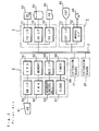
- Fig. 2 is a block diagram showing an example of the entire configuration of a microcomputer system in which the extension boards 1P and 2P as the interrupt control circuit thus constructed are built in.
- reference characters 4 and 5 designate peripheral device control boards and numeral 6 designates a central processing unit board (hereinafter referred to as a CPU board) as a control processing unit.
- reference characters 1P and 2P designate the extension board aforementioned.
- the peripheral device control boards 4 and 5, CPU board 6 and extension boards 1P and 2P are interconnected by the system bus 3.
- a floppy-disk interface 41 for floppy-disk drive unit 82, a hard-disk interface 42 for hard-disk unit 83 and a printer interface 43 for printer 84 are included.
- a display interface 51 for CRT display unit 85 and a mouse interface 52 for mouse 85 are provided.
- a CPU (Central Processing Unit) 61 for executing control processings of the entire system, a memory 62 storing programs and data for the CPU 61, an interrupt control unit 63 for controlling interruption to the CPU 61, a DMA control unit 64 for controlling at Direct Memory Access (DMA), a key-board interface 65 for key-board 81, a timer 66 for timing control, a clock 67 etc. are included.
- Respective component elements of the CPU board 6 are interconnected by an internal bus 68.
- the entire CPU board 6 and the system bus 3 are connected by a bus interface 69.
- Fig. 3 is an explanatory view showing allocation of the interrupt request input in the microcomputer system thus constructed.
- the interrupt request input signal is prepared eight from “0” to “7”, to seven signals among which from “0” to “6", the system timer 66, key-board 81, clock 67, printer 81, mouse 86, hard-disk unit 83 and floppy-disk unit 83 are already allocated in order. Therefore, the extension boards 1P and 2P use the remains one signal "7" in common.
- Fig. 4 is a flow chart showing processing sequences for interrupt request from the extension boards 1P and 2P processed by the CPU 61
- Fig. 5 is a timing chart showing the state of respective signals in the extension boards 1P and 2P.
- the fourth interrupt request line 24 of the fourth interrupt request unit 22 shown in Fig. 5(d) turns to a high level and the output of the OR gate 25 also is changed to high level.
- the output signal of the OR gate 25 is outputted to the interrupt signal line 31 from the inverter gate 26.
- the inverter gate 26 is the open collector output and wire-ORed to the interrupt signal line 31, a level of the interrupt request signal outputted to the interrupt signal line 31 changes, as shown in Fig. 5(e), to a low level which is a request level from a high level which is a normal level.
- the interrupt control unit 63 of the CPU board 6 receives the interrupt request signal outputted to the system bus 3 in the manner aforementioned via the bus interface 69, and when detecting an falling edge from the high level to the low level, transmits to the CPU 61 that the extension board 1P or 2P is generating the interrupt request (at the timing T51).
- the CPU 61 upon detecting that the interrupt request is generated, suspends processing executed at that time point for a while, and executes the interrupt processing of the sequences shown in Fig. 4.
- the CPU 61 first at the timing T52, judges whether the generated interrupt request is from the first interrupt request unit 11 or not (step ST1). In the case where the result is "YES”, though the CPU 61 executes interrupt processing for the interrupt request generated from the first interrupt request unit 11 (step ST2), the processing is moved to step ST5 since the judgment result of this case is "NO".
- step ST3 judges whether the generated interrupt request is from the second interrupt request unit 12 or not (step ST3). In the case where the result of step ST3 is "YES”, though the CPU 61 executes interrupt processing for the interrupt request generated from the second interrupt request unit (step ST4), the processing is moved to step ST5 since the judgment result of this case is "NO".
- step ST7 judges whether the generated interrupt request is from the fourth interrupt request unit 22 or not. In this case, since the result of step ST7 is "YES", the CPU 61, during the period from the timing T56 to the timing T57, executes interrupt processing for interrupt request generated from the fourth interrupt request unit 22 (step ST8), thereby one sequence of interrupt processings are completed.
- the CPU 61 Upon completion of the above interrupt processings, the CPU 61 again starts the processings being suspended before according to the program instructions, and the fourth interrupt request unit 22 returns the level of output signal to the fourth interrupt request line 24 from the high level to low level.
- the level of the third interrupt request unit 23 is changed to the high level at that time point. Accordingly, as shown in Fig. 5(e), even after the interrupt processing for interrupt request from the fourth interrupt request unit 22 is completed and the level of the fourth interrupt request line 24 returns to the low level, the interrupt request signal outputted to the interrupt signal line 31 remains at low level and is unchanged.
- the interrupt control unit 63 of the CPU board 6 Since the interrupt control unit 63 of the CPU board 6 is operated in an edge-trigger mode as aforementioned, a change of the interrupt request signal from the normal level to the request level, that is, in this conventional example, a change from the high level to the low level is only detected as the interrupt request. Therefore, the interrupt request from the third interrupt request unit 21 is not accepted by the CPU 61. Furthermore, even when the interrupt request from the third interrupt request unit 21 is locked as it is, and the interrupt request from the other interrupt request units 11, 12 or 22 is generated thereafter, these can not be accepted.
- this interrupt request signal must be sustained until the CPU 61 accepts the interrupt request. Therefore, a technical difficulty is encountered, because how long the one-shot pulse must be sustained is uncertain.
- the present invention has been designed in view of the circumstances described above, therefore, it is a primary object thereof to provide an interrupt control circuit and a microcomputer system comprising the same, which is able to, in the case where a plurality of interrupt requests are generated at delicate timings, accept them reliably and solve the problem of overhead.
- the interrupt control circuit includes, detecting means for detecting that a predetermined signal indicating the completion of interrupt processing for interrupt request is received from the control processing unit, and level changing means for changing the interrupt request signal outputted to the interrupt signal line instantaneously and forcibly to the normal level, in the case where the detecting means detects the predetermined signal.
- the microcomputer system of the present invention also includes the aforesaid interrupt control circuit and a control processing unit (CPU) which is connected to the interrupt control circuit and executes the interrupt processing.
- CPU control processing unit
- the interrupt control circuit and the microcomputer system of the present invention even in the case where the interrupt request is generated from the other interrupt request unit during execution of the requested interrupt processing, when the interrupt request circuit receives a predetermined signal indicating that the interrupt processing being executed is completed from the control processing unit, since the interrupt request signal is once changed forcibly to the normal level, it is changed again to the request level when a plurality of interrupt request signals are outputted, so that the interrupt request is prevented from being locked and in the control processing unit, the plurality of interrupt requests generated at delicate timings are accepted reliably, thus the problem of overhead is solved.
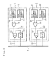
- Fig. 6 is a block diagram showing one embodiment of a configuration of an interrupt control circuit of the present invention.
- reference characters 1 and 2 respectively designate extension boards as interrupt control circuits of the present invention.
- the extension boards 1 and 2 are respectively connected to a system bus 3 by an interrupt signal line 31 which is one of the signal lines thereof.
- the extension boards 1 and 2 are constructed as follows.
- Reference characters 11 and 12 designate first and second interrupt request units provided on the extension board 1
- numerals 21 and 22 designate third and fourth interrupt request units provided on the extension board 2.
- first, second, third and fourth interrupt request lines 13, 14, 23 and 24 are connected respectively.
- the first and second interrupt request lines 13 and 14 of the first and second interrupt request units 11 and 12 are inputted to a two-input OR gate 15, and the third and fourth interrupt request lines 23 and 24 of the third and fourth interrupt request units 21 and 22 are inputted to a two-input OR gate 25.
- the OR gate 15 obtains an OR signal by OR logical operation of the interrupt request lines 13 and 14 and outputs it to one input terminal of a NAND gate 19 of the open-collector output of a forced return circuit 17, and the OR gate 25 obtains an OR signal by OR logical operation of the interrupt request lines 23 and 24 and outputs it to one input terminal of a NAND gate 29 of the open collector output of a forced return circuit 27.
- the forced return circuits 17 and 27 are constituted by the aforesaid NAND gates 19 and 29 and flip-flops 18 and 28.
- NAND gates 19 and 29 To one input terminal of the NAND gates 19 and 29, outputs from the OR gates 15 and 25 are inputted respectively as stated above, and to the other input terminal, output signals of the flip-flops 18 and 28 are inputted.
- the outputs of the NAND gates 19 and 29 are both connected to the interrupt signal lines 31.
- inputs of the flip-flops 18 and 28 are connected to the system bus 3.
- the flip-flops 18 and 28 are allocated a same address, and function as a flag of the CPU 61.
- the flip-flops 18 and 28 are simultaneously set and reset with the CPU 61 by outputting the signal indicating the completion of requested interrupt processing to the system bus 3 with the address allocated to the flip-flops 18 and 28.
- the set/reset output of the flip-flops 18 and 28 are given to the NAND gates 19 and 29.
- the extension boards 1 and 2 which are the interrupt control circuits of the present invention are, as a block diagram of Fig. 7 showing its configuration, built in a microcomputer system of the present invention having the same configuration as the conventional one shown in Fig. 2 stated above and used, except substituting for the extension boards 1P and 2P.
- allocation of the interrupt request input in the microcomputer system of the present invention, wherein the interrupt control circuit of the present invention is built in is same as the conventional one shown in Fig. 3 as aforementioned.
- Fig. 8 is a flow chart showing interrupt processing sequences for interrupt request from the extension boards 1 and 2, which are the interrupt control circuits of the present invention processed by the CPU 61
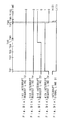
- Fig. 9 is a timing chart showing states of respective signals in the extension boards 1 and 2.
- the fourth interrupt request line 24 of the fourth interrupt request unit 22 is changed to a high level shown in Fig. 9(d).
- the flip-flops 18 and 28 are usually in the set state, that is, the output signals to the NAND gates 19 and 29 therefrom are in the high level state. Accordingly, though the output signal from the OR gate 25 is outputted as it is to the interrupt signal line 31 from the NAND gate 29, which is an open collector output and wire-ORed to the interrupt signal line 31, so that a level of the interrupt request signal outputted to the interrupt signal line 31 is changed to a low level which is the request level from a high level as the normal level.
- the interrupt control unit 63 of the CPU board 6 receives the interrupt request signal outputted to the system bus 3 via the bus interface 69 in the same manner as the conventional case stated above, and when detecting the falling edge from the high level to the low level at timing T91, transmits to the CPU 61 that the interrupt request is generated from the extension board 1 or 2.
- the CPU 61 Upon detecting that the interrupt request is generated, the CPU 61 suspends the processing being executed at that time point for a while, and executes the interrupt processing of the sequences shown in a flow chart of Fig. 8.
- the CPU 61 first, at timing T92, judges whether the generated interrupt request is from the first interrupt request unit 11 or not (step ST11). In the case where the result of step ST11 is "YES”, the CPU 61 executes the interrupt processing for generated interrupt request from the first interrupt request unit 11 (step ST12), and thereafter processes set/reset of the flag at step ST19, but since this case is "NO", the processing is moved to step ST13.
- step ST13 judges whether the generated interrupt request is from the second interrupt request unit 12 or not (step ST13). In the case where the result of step ST13 is "YES”, the CPU 61 executes the interrupt processing for generated interrupt request from the second interrupt unit 12 (step ST14), and thereafter, processes set/reset of the flag at step ST19, but since this case is "NO", the processing is moved to step ST15.
- step ST17 judges whether the generated interrupt request is from the fourth interrupt request unit 22 or not (step ST17). In this case, the result of step ST17 is "YES", so that the CPU 61 executes the interrupt processing for generated interrupt request from the fourth interrupt request unit 22 during the timings T96 to the T97 (step ST18). Thereafter, the CPU 61 processes set/reset of the flag at step ST19 during the timings T98 to T99, thereby one sequence of interrupt processings are completed.
- the CPU 61 Upon completion of the aforesaid interrupt processings, the CPU 61, according to the program instructions, again starts the processing being suspended before, and the fourth interrupt request unit 22 returns the output signal level to the fourth interrupt request line 24 from the high to low level.
- the level of the third interrupt request unit 23 is changed to the high level at that time point.
- the interrupt request signal on the interrupt signal line 31 which is the output of the NAND gates 19 and 29, as shown in Fig. 9(e)
- instantaneously returns to the high level as the normal level, and immediately thereafter, again changes to the low level as the request level.
- the interrupt control unit 63 of the CPU board 6 Since the interrupt control unit 63 of the CPU board 6 is operated in an edge-trigger mode as stated above, a change of the level of interrupt request signal to the request level from the normal level, or a change to the low level from the high level is only detected as the interrupt request. Therefore, the interrupt request from the third interrupt request unit 21 is also accepted reliably by the CPU 61 at timing T100.
- step ST12, ST14, ST16 or ST18 whenever the interrupt request from one of the interrupt request units 11, 12, 21 or 22 is processed in step ST12, ST14, ST16 or ST18, a flag is set or reset in step ST19 and a series of processings are completed. Accordingly, even in the case wherein the interrupt requests are generated simultaneously from each of the interrupt request units 11, 12, 21 and 22, when one interrupt request has been processed, it is possible to execute the interrupt processing for interrupt request which is generated immediately thereafter and has a higher priority.
- the time necessary for the CPU 61 to detect the interrupt request and execute the set/reset processing is by far shorter than the time necessary for executing the interrupt processing itself, so that the processing time for one interrupt request may not be prolonged more than necessity.
- interrupt factors are checked successively, it may be constructed, naturally, such that the interrupt factors are taken in by one input/output instruction with the same input address.
- the time necessary for detecting the interrupt request is more shortened.
- an interrupt control circuit and a microcomputer system comprising the same, it is so constructed that the level of the interrupt request signal is instantaneously changed forcibly to a normal level from a request level, when the CPU receives the signal indicating the completion of interrupt processing being executed, so that the interrupt request is not locked and the interrupt requests generated continuously at delicate timings can be accepted reliably, and further, the time necessary for interrupt processing for interrupt request is shortened, thereby a problem of overhead seen in the conventional example is solved.
Landscapes
- Engineering & Computer Science (AREA)
- Theoretical Computer Science (AREA)
- Physics & Mathematics (AREA)
- General Engineering & Computer Science (AREA)
- General Physics & Mathematics (AREA)
- Bus Control (AREA)
Abstract
Description
- The present invention relates to an interrupt control circuit and a microcomputer system comprising the same for generating an interrupt request signal for a control processing unit operating under an edge-trigger mode.
- Fig. 1 is a block diagram showing an example of configuration of a conventional interrupt control circuit.
- In Fig. 1,
reference characters - The
extension boards system bus 3 by aninterrupt signal line 31 which is one of the signal lines thereof. - The
extension boards Reference characters 11 and 12 designate a first and a second interrupt request units provided on theextension board 1P, andnumerals extension board 2P. To the respectiveinterrupt request units interrupt request lines - The first and second
interrupt request lines interrupt request units 11 and 12 are inputted to a two-input OR gate 15, and the third and fourthinterrupt request lines interrupt request units input OR gate 25. TheOR gate 15 outputs the OR signal of theinterrupt request lines inverter gate 16 of the open collector output, and theOR gate 25 outputs the OR signal of theinterrupt request lines inverter gate 26 of the open collector output. Outputs of theinverter gates 16 and 17 are wire-ORed to thesystem bus 3 via theinterrupt signal lines 31. - Fig. 2 is a block diagram showing an example of the entire configuration of a microcomputer system in which the
extension boards - In Fig. 2,
reference characters numeral 6 designates a central processing unit board (hereinafter referred to as a CPU board) as a control processing unit. In addition,reference characters device control boards CPU board 6 andextension boards system bus 3. - In the peripheral
device control board 4, a floppy-disk interface 41 for floppy-disk drive unit 82, a hard-disk interface 42 for hard-disk unit 83 and aprinter interface 43 forprinter 84 are included. - On the peripheral
device control board 5, adisplay interface 51 forCRT display unit 85 and a mouse interface 52 formouse 85 are provided. - In the
CPU board 6, a CPU (Central Processing Unit) 61 for executing control processings of the entire system, amemory 62 storing programs and data for the CPU 61, aninterrupt control unit 63 for controlling interruption to the CPU 61, aDMA control unit 64 for controlling at Direct Memory Access (DMA), a key-board interface 65 for key-board 81, atimer 66 for timing control, a clock 67 etc. are included. Respective component elements of theCPU board 6 are interconnected by aninternal bus 68. Theentire CPU board 6 and thesystem bus 3 are connected by abus interface 69. - Fig. 3 is an explanatory view showing allocation of the interrupt request input in the microcomputer system thus constructed.
- As shown in Fig. 3, the interrupt request input signal is prepared eight from "0" to "7", to seven signals among which from "0" to "6", the
system timer 66, key-board 81, clock 67,printer 81,mouse 86, hard-disk unit 83 and floppy-disk unit 83 are already allocated in order. Therefore, theextension boards - Next, the interrupt processing of the conventional microcomputer system as above constructed will be described.
- Incidentally, Fig. 4 is a flow chart showing processing sequences for interrupt request from the
extension boards extension boards - Now, for example, when the interrupt request is generated from the fourth
interrupt request unit 22, the fourthinterrupt request line 24 of the fourthinterrupt request unit 22 shown in Fig. 5(d) turns to a high level and the output of theOR gate 25 also is changed to high level. The output signal of the ORgate 25 is outputted to theinterrupt signal line 31 from theinverter gate 26. At this time, since theinverter gate 26 is the open collector output and wire-ORed to theinterrupt signal line 31, a level of the interrupt request signal outputted to theinterrupt signal line 31 changes, as shown in Fig. 5(e), to a low level which is a request level from a high level which is a normal level. - The
interrupt control unit 63 of theCPU board 6 receives the interrupt request signal outputted to thesystem bus 3 in the manner aforementioned via thebus interface 69, and when detecting an falling edge from the high level to the low level, transmits to the CPU 61 that theextension board - The CPU 61 upon detecting that the interrupt request is generated, suspends processing executed at that time point for a while, and executes the interrupt processing of the sequences shown in Fig. 4.
- Specifically, the CPU 61, first at the timing T52, judges whether the generated interrupt request is from the first interrupt request unit 11 or not (step ST1). In the case where the result is "YES", though the CPU 61 executes interrupt processing for the interrupt request generated from the first interrupt request unit 11 (step ST2), the processing is moved to step ST5 since the judgment result of this case is "NO".
- Next, the CPU 61, at timing T53, judges whether the generated interrupt request is from the second
interrupt request unit 12 or not (step ST3). In the case where the result of step ST3 is "YES", though the CPU 61 executes interrupt processing for the interrupt request generated from the second interrupt request unit (step ST4), the processing is moved to step ST5 since the judgment result of this case is "NO". - In the same manner, the CPU 61, at timing T55, judges whether the generated interrupt request is from the fourth
interrupt request unit 22 or not (step ST7). In this case, since the result of step ST7 is "YES", the CPU 61, during the period from the timing T56 to the timing T57, executes interrupt processing for interrupt request generated from the fourth interrupt request unit 22 (step ST8), thereby one sequence of interrupt processings are completed. - Upon completion of the above interrupt processings, the CPU 61 again starts the processings being suspended before according to the program instructions, and the fourth
interrupt request unit 22 returns the level of output signal to the fourthinterrupt request line 24 from the high level to low level. - Here, in the case where the interrupt request is generated from the third
interrupt request unit 21, between the timing T54 where the CPU 61 judges ("NO"), i.e. the interrupt request is not from the thirdinterrupt request unit 21 in step ST5, and the timing T57 where the interrupt processing for interrupt request from the fourthinterrupt request unit 22 is completed, as shown in Fig. 5(c), the level of the thirdinterrupt request unit 23 is changed to the high level at that time point. Accordingly, as shown in Fig. 5(e), even after the interrupt processing for interrupt request from the fourthinterrupt request unit 22 is completed and the level of the fourthinterrupt request line 24 returns to the low level, the interrupt request signal outputted to theinterrupt signal line 31 remains at low level and is unchanged. - Since the
interrupt control unit 63 of theCPU board 6 is operated in an edge-trigger mode as aforementioned, a change of the interrupt request signal from the normal level to the request level, that is, in this conventional example, a change from the high level to the low level is only detected as the interrupt request. Therefore, the interrupt request from the thirdinterrupt request unit 21 is not accepted by the CPU 61. Furthermore, even when the interrupt request from the thirdinterrupt request unit 21 is locked as it is, and the interrupt request from the otherinterrupt request units - Though it may be considered to output the interrupt request signal to the
interrupt signal line 31 in one-shot pulse, this interrupt request signal must be sustained until the CPU 61 accepts the interrupt request. Therefore, a technical difficulty is encountered, because how long the one-shot pulse must be sustained is uncertain. - Since the aforesaid configuration is adopted in the conventional interrupt control circuit, when the interrupt requests from the
interrupt request units interrupt signal line 31 in common are generated successively at delicate timings, there is a possibility that some of them are not accepted by the CPU 61. There is also a difficulty in a system, wherein a rapid response is required because of the necessity of processing all interrupt requests generated simultaneously in theinterrupt request units interrupt signal lines 31 are used in common in a number of interrupt request units, such a problem is encountered that an overhead of interrupt requests generated simultaneously becomes problematic and the number of interrupt requests can not be increased more than a certain extent. - The present invention has been designed in view of the circumstances described above, therefore, it is a primary object thereof to provide an interrupt control circuit and a microcomputer system comprising the same, which is able to, in the case where a plurality of interrupt requests are generated at delicate timings, accept them reliably and solve the problem of overhead.
- The interrupt control circuit according to the present invention includes, detecting means for detecting that a predetermined signal indicating the completion of interrupt processing for interrupt request is received from the control processing unit, and level changing means for changing the interrupt request signal outputted to the interrupt signal line instantaneously and forcibly to the normal level, in the case where the detecting means detects the predetermined signal.
- The microcomputer system of the present invention also includes the aforesaid interrupt control circuit and a control processing unit (CPU) which is connected to the interrupt control circuit and executes the interrupt processing.
- In the interrupt control circuit and the microcomputer system of the present invention, even in the case where the interrupt request is generated from the other interrupt request unit during execution of the requested interrupt processing, when the interrupt request circuit receives a predetermined signal indicating that the interrupt processing being executed is completed from the control processing unit, since the interrupt request signal is once changed forcibly to the normal level, it is changed again to the request level when a plurality of interrupt request signals are outputted, so that the interrupt request is prevented from being locked and in the control processing unit, the plurality of interrupt requests generated at delicate timings are accepted reliably, thus the problem of overhead is solved.
- The above and further objects and features of the invention will more fully by apparent from the following detailed description with accompanying drawings.
-
- Fig. 1 a block diagram showing an example of the configuration of a conventional interrupt control circuit,
- Fig. 2 is a block diagram showing an example of the entire configuration of a conventional microcomputer system wherein the interrupt control circuit of the configuration of Fig. 1 is built in,
- Fig. 3 is an explanatory view showing allocation of the interrupt request input in the conventional microcomputer system of the configuration of Fig. 2,
- Fig. 4 is a flow chart showing processing sequences for interrupt request from an interrupt request circuit processed by a control processing unit (CPU),
- Fig. 5 is a timing chart showing states of respective signals in the interrupt control circuit,
- Fig. 6 is a block diagram showing one embodiment of the configuration of an interrupt control circuit of the present invention,
- Fig. 7 is a block diagram showing an example of the entire configuration of a microcomputer system of the present invention, wherein the interrupt control circuit of the present invention of the configuration shown in Fig. 6 is built in,
- Fig. 8 is a flow chart showing interrupt processing sequences for interrupt request from the interrupt control circuit of the present invention processed by the control processing unit (CPU), and
- Fig. 9 is a timing chart showing states of respective signals in the
interrupt control circuit 2. - In the following, the present invention will be described in detail with reference to the drawings showing its embodiments.
- Fig. 6 is a block diagram showing one embodiment of a configuration of an interrupt control circuit of the present invention.
- In Fig. 6,
reference characters extension boards system bus 3 by an interruptsignal line 31 which is one of the signal lines thereof. - The
extension boards Reference characters 11 and 12 designate first and second interrupt request units provided on theextension board 1, andnumerals extension board 2. To the interruptrequest units request lines - The first and second interrupt
request lines request units 11 and 12 are inputted to a two-input ORgate 15, and the third and fourth interruptrequest lines request units gate 25. TheOR gate 15 obtains an OR signal by OR logical operation of the interruptrequest lines NAND gate 19 of the open-collector output of a forced return circuit 17, and theOR gate 25 obtains an OR signal by OR logical operation of the interruptrequest lines NAND gate 29 of the open collector output of a forcedreturn circuit 27. - The forced
return circuits 17 and 27, upon receiving the interrupt completion signal which is outputted when the CPU 61 completes the requested interrupt processing, instantaneously returns the interrupt request signal outputted to the interruptsignal line 31 forcibly to a normal level or a high level. - Specifically, the forced
return circuits 17 and 27 are constituted by theaforesaid NAND gates flops NAND gates gates flops NAND gates signal lines 31. Meanwhile, inputs of the flip-flops system bus 3. The flip-flops flops system bus 3 with the address allocated to the flip-flops flops NAND gates - The
extension boards extension boards - Next, the interrupt processing of the microcomputer system wherein the interrupt control circuit of the present invention having the aforesaid configuration is built in will be explained.
- Here, Fig. 8 is a flow chart showing interrupt processing sequences for interrupt request from the
extension boards extension boards - Now, for example, when the interrupt request is generated from the fourth interrupt
request unit 22, the fourth interruptrequest line 24 of the fourth interruptrequest unit 22 is changed to a high level shown in Fig. 9(d). Here, the flip-flops NAND gates OR gate 25 is outputted as it is to the interruptsignal line 31 from theNAND gate 29, which is an open collector output and wire-ORed to the interruptsignal line 31, so that a level of the interrupt request signal outputted to the interruptsignal line 31 is changed to a low level which is the request level from a high level as the normal level. - The interrupt
control unit 63 of theCPU board 6 receives the interrupt request signal outputted to thesystem bus 3 via thebus interface 69 in the same manner as the conventional case stated above, and when detecting the falling edge from the high level to the low level at timing T91, transmits to the CPU 61 that the interrupt request is generated from theextension board - Upon detecting that the interrupt request is generated, the CPU 61 suspends the processing being executed at that time point for a while, and executes the interrupt processing of the sequences shown in a flow chart of Fig. 8.
- Specifically, the CPU 61, first, at timing T92, judges whether the generated interrupt request is from the first interrupt request unit 11 or not (step ST11). In the case where the result of step ST11 is "YES", the CPU 61 executes the interrupt processing for generated interrupt request from the first interrupt request unit 11 (step ST12), and thereafter processes set/reset of the flag at step ST19, but since this case is "NO", the processing is moved to step ST13.
- Next, the CPU 61, at timing T93, judges whether the generated interrupt request is from the second interrupt
request unit 12 or not (step ST13). In the case where the result of step ST13 is "YES", the CPU 61 executes the interrupt processing for generated interrupt request from the second interrupt unit 12 (step ST14), and thereafter, processes set/reset of the flag at step ST19, but since this case is "NO", the processing is moved to step ST15. - In the same manner, the CPU 61, at timing T95, judges whether the generated interrupt request is from the fourth interrupt
request unit 22 or not (step ST17). In this case, the result of step ST17 is "YES", so that the CPU 61 executes the interrupt processing for generated interrupt request from the fourth interruptrequest unit 22 during the timings T96 to the T97 (step ST18). Thereafter, the CPU 61 processes set/reset of the flag at step ST19 during the timings T98 to T99, thereby one sequence of interrupt processings are completed. - Upon completion of the aforesaid interrupt processings, the CPU 61, according to the program instructions, again starts the processing being suspended before, and the fourth interrupt
request unit 22 returns the output signal level to the fourth interruptrequest line 24 from the high to low level. - Here, in the case where the interrupt request is generated from the third interrupt
request unit 21, between the timing T94 where the CPU 61 judges "NO", i.e. the interrupt request is not from the third interruptrequest unit 21, and the timing T97 where the interrupt processing for interrupt request from the fourth interruptrequest unit 22 is completed, as shown in Fig. 9(c), the level of the third interruptrequest unit 23 is changed to the high level at that time point. In the present invention, however, by resetting the flip-flops signal line 31 which is the output of theNAND gates - Since the interrupt
control unit 63 of theCPU board 6 is operated in an edge-trigger mode as stated above, a change of the level of interrupt request signal to the request level from the normal level, or a change to the low level from the high level is only detected as the interrupt request. Therefore, the interrupt request from the third interruptrequest unit 21 is also accepted reliably by the CPU 61 at timing T100. - As shown in a flow chart of Fig. 8, whenever the interrupt request from one of the interrupt
request units request units - In the aforesaid embodiment, as shown in a flow chart of Fig. 8, though interrupt factors are checked successively, it may be constructed, naturally, such that the interrupt factors are taken in by one input/output instruction with the same input address. When thus constructed, the time necessary for detecting the interrupt request is more shortened.
- As particularly described heretofore, in an interrupt control circuit and a microcomputer system comprising the same, it is so constructed that the level of the interrupt request signal is instantaneously changed forcibly to a normal level from a request level, when the CPU receives the signal indicating the completion of interrupt processing being executed, so that the interrupt request is not locked and the interrupt requests generated continuously at delicate timings can be accepted reliably, and further, the time necessary for interrupt processing for interrupt request is shortened, thereby a problem of overhead seen in the conventional example is solved.
- As this invention may be embodied in several forms without departing from the spirit of essential characteristics thereof, the present embodiment is therefore illustrative and not restrictive, since the scope of the invention is defined by the appended claims rather than by the description preceding them, and all changes that fall within metes and bounds of the claims, or equivalence of such metes and bounds thereof are therefore intended to be embraced by the claims.
Claims (4)
- An interrupt control circuit (1, 2) for requesting interrupt processing to a control processing unit (61) by changing a level of an interrupt request signal from one level to the another, said control processing unit (61) being constituted in an edge-trigger mode under which generation of the interrupt request is detected by detecting a level change of said interrupt request signal, and outputting a predetermined signal in the case where the interrupt processing is completed after detecting the generation of the interrupt request and executing the interrupt processing, characterized by comprising:
detecting means (18, 28) for detecting said predetermined signal outputted from said control processing unit (61); and
level changing means (19, 29) for changing said interrupt request signal temporarily to said one level, in the case where said detecting means (18, 28) detects said predetermined signal. - An interrupt control circuit (1, 2) as set forth in claim 1, wherein
said detecting means (18, 28) is composed of a flip-flop is set/reset by a signal outputted from said control processing unit (61) at completion of interrupt processing, and
said level changing means (19, 29) is composed of a logical gate whose inputs are the output of said flip-flop (18, 28) and output of said interrupt request signal,
whereby the output of said logical gate (19, 29) is changed temporarily to said one level responsive to set/reset of said flip-flop 18, 28). - A microcomputer system, comprising: a control processing unit (61) which is constituted in an edge-trigger mode under which generation of the interrupt request is detected by detecting a level change of an interrupt request signal, and outputs a predetermined signal in the case where the interrupt processing is completed after detecting the generation of the interrupt request and executing the interrupt processing, and an interrupt control circuit (1, 2), for requesting an interrupt processing by detecting change of the level of the interrupt request signal from one level to the another, characterized in that
said interrupt control circuit (1, 2) has detecting means (18, 28) for detecting said predetermined signal outputted from said control processing unit (61), and level changing means (19, 29) for changing said interrupt request signal temporarily to said one level in the case where said detecting means (18, 28) detects said predetermined signal. - A microcomputer system as set forth in claim 3, wherein
said detecting means (18, 28) is composed of a flip-flop which is set/reset by a signal outputted from said control processing unit (61) at completion of interrupt processing, and
said level changing means (19, 29) is composed of a logical gate (19, 29) whose inputs are the output of said flip-flop (18, 28) and said interrupt request signal,
whereby the output of said logical gate (19, 29) is changed temporarily to said one level responsive to set/reset of said flip-flop (18, 28).
Applications Claiming Priority (2)
| Application Number | Priority Date | Filing Date | Title |
|---|---|---|---|
| JP109869/90 | 1990-04-25 | ||
| JP10986990A JPH047641A (en) | 1990-04-25 | 1990-04-25 | Interruption control device |
Publications (3)
| Publication Number | Publication Date |
|---|---|
| EP0454096A2 true EP0454096A2 (en) | 1991-10-30 |
| EP0454096A3 EP0454096A3 (en) | 1992-05-20 |
| EP0454096B1 EP0454096B1 (en) | 1997-07-30 |
Family
ID=14521261
Family Applications (1)
| Application Number | Title | Priority Date | Filing Date |
|---|---|---|---|
| EP19910106612 Expired - Lifetime EP0454096B1 (en) | 1990-04-25 | 1991-04-24 | Interrupt control circuit and microcomputer system comprising the same |
Country Status (3)
| Country | Link |
|---|---|
| EP (1) | EP0454096B1 (en) |
| JP (1) | JPH047641A (en) |
| DE (1) | DE69127013T2 (en) |
Cited By (1)
| Publication number | Priority date | Publication date | Assignee | Title |
|---|---|---|---|---|
| WO1999009487A1 (en) * | 1997-08-15 | 1999-02-25 | Lsi Logic Corporation | Shared interrupt processing in a data processing system |
Citations (4)
| Publication number | Priority date | Publication date | Assignee | Title |
|---|---|---|---|---|
| EP0167827A2 (en) * | 1984-07-11 | 1986-01-15 | International Business Machines Corporation | Interrupt level sharing circuit |
| US4760516A (en) * | 1986-11-25 | 1988-07-26 | Dialogic Corporation | Peripheral interrupt interface for multiple access to an interrupt level |
| US4764893A (en) * | 1985-04-26 | 1988-08-16 | International Business Machines Corporation | Noise-immune interrupt level sharing |
| EP0358330A1 (en) * | 1988-09-09 | 1990-03-14 | Compaq Computer Corporation | Programmable interrupt controller |
Family Cites Families (2)
| Publication number | Priority date | Publication date | Assignee | Title |
|---|---|---|---|---|
| JPS62267834A (en) * | 1986-05-15 | 1987-11-20 | Matsushita Electric Ind Co Ltd | Microcomputer |
| JPS63316236A (en) * | 1987-06-19 | 1988-12-23 | Nec Corp | Interruption control circuit |
-
1990
- 1990-04-25 JP JP10986990A patent/JPH047641A/en active Pending
-
1991
- 1991-04-24 EP EP19910106612 patent/EP0454096B1/en not_active Expired - Lifetime
- 1991-04-24 DE DE1991627013 patent/DE69127013T2/en not_active Expired - Fee Related
Patent Citations (4)
| Publication number | Priority date | Publication date | Assignee | Title |
|---|---|---|---|---|
| EP0167827A2 (en) * | 1984-07-11 | 1986-01-15 | International Business Machines Corporation | Interrupt level sharing circuit |
| US4764893A (en) * | 1985-04-26 | 1988-08-16 | International Business Machines Corporation | Noise-immune interrupt level sharing |
| US4760516A (en) * | 1986-11-25 | 1988-07-26 | Dialogic Corporation | Peripheral interrupt interface for multiple access to an interrupt level |
| EP0358330A1 (en) * | 1988-09-09 | 1990-03-14 | Compaq Computer Corporation | Programmable interrupt controller |
Non-Patent Citations (2)
| Title |
|---|
| E.D.N. ELECTRONIC DESIGN NEWS vol. 27, no. 15, 4 August 1982, BOSTON, MA, US pages 137 - 142; M. TILDEN ET AL: 'GPIB software configuration determines system performance' * |
| IBM TECHNICAL DISCLOSURE BULLETIN vol. 29, no. 6, 1 November 1986, ARMONK, NY, US pages 2380 - 2381; ANONYMOUS: 'Interrupt sharing for personal computer' * |
Cited By (2)
| Publication number | Priority date | Publication date | Assignee | Title |
|---|---|---|---|---|
| WO1999009487A1 (en) * | 1997-08-15 | 1999-02-25 | Lsi Logic Corporation | Shared interrupt processing in a data processing system |
| US6003109A (en) * | 1997-08-15 | 1999-12-14 | Lsi Logic Corporation | Method and apparatus for processing interrupts in a data processing system |
Also Published As
| Publication number | Publication date |
|---|---|
| EP0454096B1 (en) | 1997-07-30 |
| EP0454096A3 (en) | 1992-05-20 |
| JPH047641A (en) | 1992-01-13 |
| DE69127013T2 (en) | 1998-01-22 |
| DE69127013D1 (en) | 1997-09-04 |
Similar Documents
| Publication | Publication Date | Title |
|---|---|---|
| US4112490A (en) | Data transfer control apparatus and method | |
| EP0263886B1 (en) | Interrupt control method in a multiprocessor system | |
| EP0166272B1 (en) | Processor bus access | |
| EP0458304B1 (en) | Direct memory access transfer controller and use | |
| KR940011670B1 (en) | Interrupt controller | |
| EP0597441A1 (en) | Microprocessor having a bus-width change function | |
| EP0786726A2 (en) | Interrupt sharing technique for PCMCIA cards | |
| US5274780A (en) | Bus controller for adjusting a bus master to a bus slave | |
| JP2634130B2 (en) | Method and computer system for controlling use of a bus | |
| US4729090A (en) | DMA system employing plural bus request and grant signals for improving bus data transfer speed | |
| EP1063594B1 (en) | An interrupt controller and a microcomputer incorporating this controller | |
| EP0418932A2 (en) | Microcomputer having easily testable interrupt controller | |
| KR900004291B1 (en) | A method and apparatus for coordinating exceution of an instruction by a processor | |
| EP0094140A1 (en) | Data processing system with system bus for transfer of information | |
| US5305442A (en) | Generalized hierarchical architecture for bus adapters | |
| US5247640A (en) | Dual access control system including plural magnetic disk control units and contention control circuitry | |
| US5261083A (en) | Floppy disk controller interface for suppressing false verify cycle errors | |
| EP0454096A2 (en) | Interrupt control circuit and microcomputer system comprising the same | |
| US5761482A (en) | Emulation apparatus | |
| US4259717A (en) | Information processor | |
| EP0706136B1 (en) | Interface between a cpu and an interrupt controller | |
| US5748909A (en) | Interface board and instruction processing device without a local CPU | |
| JP3093374B2 (en) | Interrupt controller | |
| JP2754594B2 (en) | Single chip microcomputer | |
| JPS63228856A (en) | Communication controller |
Legal Events
| Date | Code | Title | Description |
|---|---|---|---|
| PUAI | Public reference made under article 153(3) epc to a published international application that has entered the european phase |
Free format text: ORIGINAL CODE: 0009012 |
|
| AK | Designated contracting states |
Kind code of ref document: A2 Designated state(s): DE FR GB |
|
| PUAL | Search report despatched |
Free format text: ORIGINAL CODE: 0009013 |
|
| AK | Designated contracting states |
Kind code of ref document: A3 Designated state(s): DE FR GB |
|
| 17P | Request for examination filed |
Effective date: 19921111 |
|
| 17Q | First examination report despatched |
Effective date: 19950629 |
|
| GRAG | Despatch of communication of intention to grant |
Free format text: ORIGINAL CODE: EPIDOS AGRA |
|
| GRAH | Despatch of communication of intention to grant a patent |
Free format text: ORIGINAL CODE: EPIDOS IGRA |
|
| GRAH | Despatch of communication of intention to grant a patent |
Free format text: ORIGINAL CODE: EPIDOS IGRA |
|
| GRAA | (expected) grant |
Free format text: ORIGINAL CODE: 0009210 |
|
| AK | Designated contracting states |
Kind code of ref document: B1 Designated state(s): DE FR GB |
|
| REF | Corresponds to: |
Ref document number: 69127013 Country of ref document: DE Date of ref document: 19970904 |
|
| ET | Fr: translation filed | ||
| PLBE | No opposition filed within time limit |
Free format text: ORIGINAL CODE: 0009261 |
|
| STAA | Information on the status of an ep patent application or granted ep patent |
Free format text: STATUS: NO OPPOSITION FILED WITHIN TIME LIMIT |
|
| 26N | No opposition filed | ||
| REG | Reference to a national code |
Ref country code: GB Ref legal event code: 746 Effective date: 19990519 |
|
| REG | Reference to a national code |
Ref country code: FR Ref legal event code: D6 |
|
| REG | Reference to a national code |
Ref country code: GB Ref legal event code: IF02 |
|
| PGFP | Annual fee paid to national office [announced via postgrant information from national office to epo] |
Ref country code: FR Payment date: 20020410 Year of fee payment: 12 |
|
| PGFP | Annual fee paid to national office [announced via postgrant information from national office to epo] |
Ref country code: GB Payment date: 20020424 Year of fee payment: 12 |
|
| PGFP | Annual fee paid to national office [announced via postgrant information from national office to epo] |
Ref country code: DE Payment date: 20020502 Year of fee payment: 12 |
|
| PG25 | Lapsed in a contracting state [announced via postgrant information from national office to epo] |
Ref country code: GB Free format text: LAPSE BECAUSE OF NON-PAYMENT OF DUE FEES Effective date: 20030424 |
|
| PG25 | Lapsed in a contracting state [announced via postgrant information from national office to epo] |
Ref country code: DE Free format text: LAPSE BECAUSE OF NON-PAYMENT OF DUE FEES Effective date: 20031101 |
|
| GBPC | Gb: european patent ceased through non-payment of renewal fee | ||
| PG25 | Lapsed in a contracting state [announced via postgrant information from national office to epo] |
Ref country code: FR Free format text: LAPSE BECAUSE OF NON-PAYMENT OF DUE FEES Effective date: 20031231 |
|
| REG | Reference to a national code |
Ref country code: FR Ref legal event code: ST |