EP0453615A1 - A preparation method of bulk Y-Ba-Cu-O superconductors with high transport critical current density - Google Patents
A preparation method of bulk Y-Ba-Cu-O superconductors with high transport critical current density Download PDFInfo
- Publication number
- EP0453615A1 EP0453615A1 EP90108127A EP90108127A EP0453615A1 EP 0453615 A1 EP0453615 A1 EP 0453615A1 EP 90108127 A EP90108127 A EP 90108127A EP 90108127 A EP90108127 A EP 90108127A EP 0453615 A1 EP0453615 A1 EP 0453615A1
- Authority
- EP
- European Patent Office
- Prior art keywords
- temperature
- critical current
- current density
- pellet
- sample
- Prior art date
- Legal status (The legal status is an assumption and is not a legal conclusion. Google has not performed a legal analysis and makes no representation as to the accuracy of the status listed.)
- Granted
Links
- 239000002887 superconductor Substances 0.000 title claims abstract description 25
- 238000002360 preparation method Methods 0.000 title claims abstract description 9
- 229910009203 Y-Ba-Cu-O Inorganic materials 0.000 title 1
- 239000008188 pellet Substances 0.000 claims description 12
- 238000000137 annealing Methods 0.000 claims description 4
- 239000000843 powder Substances 0.000 claims description 2
- QVGXLLKOCUKJST-UHFFFAOYSA-N atomic oxygen Chemical compound [O] QVGXLLKOCUKJST-UHFFFAOYSA-N 0.000 claims 1
- 238000000227 grinding Methods 0.000 claims 1
- 238000002156 mixing Methods 0.000 claims 1
- 239000000203 mixture Substances 0.000 claims 1
- 229910052760 oxygen Inorganic materials 0.000 claims 1
- 239000001301 oxygen Substances 0.000 claims 1
- 238000000034 method Methods 0.000 abstract description 16
- 230000005415 magnetization Effects 0.000 description 16
- 230000004907 flux Effects 0.000 description 8
- BQCADISMDOOEFD-UHFFFAOYSA-N Silver Chemical compound [Ag] BQCADISMDOOEFD-UHFFFAOYSA-N 0.000 description 7
- 239000000463 material Substances 0.000 description 5
- IJGRMHOSHXDMSA-UHFFFAOYSA-N nitrogen Substances N#N IJGRMHOSHXDMSA-UHFFFAOYSA-N 0.000 description 5
- 239000000758 substrate Substances 0.000 description 4
- 239000013078 crystal Substances 0.000 description 3
- 238000010438 heat treatment Methods 0.000 description 3
- 238000005259 measurement Methods 0.000 description 3
- 229910052757 nitrogen Inorganic materials 0.000 description 3
- 230000008569 process Effects 0.000 description 3
- 229910052709 silver Inorganic materials 0.000 description 3
- 239000004332 silver Substances 0.000 description 3
- 238000010408 sweeping Methods 0.000 description 3
- 241000238366 Cephalopoda Species 0.000 description 2
- 235000010627 Phaseolus vulgaris Nutrition 0.000 description 2
- 244000046052 Phaseolus vulgaris Species 0.000 description 2
- 230000001419 dependent effect Effects 0.000 description 2
- 230000000694 effects Effects 0.000 description 2
- 239000007788 liquid Substances 0.000 description 2
- 238000004519 manufacturing process Methods 0.000 description 2
- 239000003973 paint Substances 0.000 description 2
- 238000010583 slow cooling Methods 0.000 description 2
- 239000010409 thin film Substances 0.000 description 2
- 238000002441 X-ray diffraction Methods 0.000 description 1
- 230000008859 change Effects 0.000 description 1
- 238000007796 conventional method Methods 0.000 description 1
- 238000001816 cooling Methods 0.000 description 1
- 230000007423 decrease Effects 0.000 description 1
- 238000002474 experimental method Methods 0.000 description 1
- 239000010408 film Substances 0.000 description 1
- 238000007429 general method Methods 0.000 description 1
- 239000007791 liquid phase Substances 0.000 description 1
- 238000012986 modification Methods 0.000 description 1
- 230000004048 modification Effects 0.000 description 1
- 238000012545 processing Methods 0.000 description 1
- 238000002310 reflectometry Methods 0.000 description 1
- 238000005245 sintering Methods 0.000 description 1
- 238000001228 spectrum Methods 0.000 description 1
- 238000009987 spinning Methods 0.000 description 1
- 238000012360 testing method Methods 0.000 description 1
- 230000007704 transition Effects 0.000 description 1
Images


Classifications
-
- C—CHEMISTRY; METALLURGY
- C04—CEMENTS; CONCRETE; ARTIFICIAL STONE; CERAMICS; REFRACTORIES
- C04B—LIME, MAGNESIA; SLAG; CEMENTS; COMPOSITIONS THEREOF, e.g. MORTARS, CONCRETE OR LIKE BUILDING MATERIALS; ARTIFICIAL STONE; CERAMICS; REFRACTORIES; TREATMENT OF NATURAL STONE
- C04B35/00—Shaped ceramic products characterised by their composition; Ceramics compositions; Processing powders of inorganic compounds preparatory to the manufacturing of ceramic products
- C04B35/01—Shaped ceramic products characterised by their composition; Ceramics compositions; Processing powders of inorganic compounds preparatory to the manufacturing of ceramic products based on oxide ceramics
- C04B35/45—Shaped ceramic products characterised by their composition; Ceramics compositions; Processing powders of inorganic compounds preparatory to the manufacturing of ceramic products based on oxide ceramics based on copper oxide or solid solutions thereof with other oxides
- C04B35/4504—Shaped ceramic products characterised by their composition; Ceramics compositions; Processing powders of inorganic compounds preparatory to the manufacturing of ceramic products based on oxide ceramics based on copper oxide or solid solutions thereof with other oxides containing rare earth oxides
- C04B35/4508—Type 1-2-3
-
- C—CHEMISTRY; METALLURGY
- C04—CEMENTS; CONCRETE; ARTIFICIAL STONE; CERAMICS; REFRACTORIES
- C04B—LIME, MAGNESIA; SLAG; CEMENTS; COMPOSITIONS THEREOF, e.g. MORTARS, CONCRETE OR LIKE BUILDING MATERIALS; ARTIFICIAL STONE; CERAMICS; REFRACTORIES; TREATMENT OF NATURAL STONE
- C04B35/00—Shaped ceramic products characterised by their composition; Ceramics compositions; Processing powders of inorganic compounds preparatory to the manufacturing of ceramic products
- C04B35/622—Forming processes; Processing powders of inorganic compounds preparatory to the manufacturing of ceramic products
- C04B35/653—Processes involving a melting step
-
- H—ELECTRICITY
- H10—SEMICONDUCTOR DEVICES; ELECTRIC SOLID-STATE DEVICES NOT OTHERWISE PROVIDED FOR
- H10N—ELECTRIC SOLID-STATE DEVICES NOT OTHERWISE PROVIDED FOR
- H10N60/00—Superconducting devices
- H10N60/01—Manufacture or treatment
- H10N60/0268—Manufacture or treatment of devices comprising copper oxide
-
- Y—GENERAL TAGGING OF NEW TECHNOLOGICAL DEVELOPMENTS; GENERAL TAGGING OF CROSS-SECTIONAL TECHNOLOGIES SPANNING OVER SEVERAL SECTIONS OF THE IPC; TECHNICAL SUBJECTS COVERED BY FORMER USPC CROSS-REFERENCE ART COLLECTIONS [XRACs] AND DIGESTS
- Y10—TECHNICAL SUBJECTS COVERED BY FORMER USPC
- Y10S—TECHNICAL SUBJECTS COVERED BY FORMER USPC CROSS-REFERENCE ART COLLECTIONS [XRACs] AND DIGESTS
- Y10S505/00—Superconductor technology: apparatus, material, process
- Y10S505/725—Process of making or treating high tc, above 30 k, superconducting shaped material, article, or device
- Y10S505/742—Annealing
-
- Y—GENERAL TAGGING OF NEW TECHNOLOGICAL DEVELOPMENTS; GENERAL TAGGING OF CROSS-SECTIONAL TECHNOLOGIES SPANNING OVER SEVERAL SECTIONS OF THE IPC; TECHNICAL SUBJECTS COVERED BY FORMER USPC CROSS-REFERENCE ART COLLECTIONS [XRACs] AND DIGESTS
- Y10—TECHNICAL SUBJECTS COVERED BY FORMER USPC
- Y10S—TECHNICAL SUBJECTS COVERED BY FORMER USPC CROSS-REFERENCE ART COLLECTIONS [XRACs] AND DIGESTS
- Y10S505/00—Superconductor technology: apparatus, material, process
- Y10S505/775—High tc, above 30 k, superconducting material
- Y10S505/776—Containing transition metal oxide with rare earth or alkaline earth
- Y10S505/779—Other rare earth, i.e. Sc,Y,Ce,Pr,Nd,Pm,Sm,Eu,Gd,Tb,Dy,Ho,Er,Tm,Yb,Lu and alkaline earth, i.e. Ca,Sr,Ba,Ra
- Y10S505/78—Yttrium and barium-, e.g. YBa2Cu307
Definitions
- the YBa2Cu3O x superconductor formed possesses high transport Ic and Jc.
- the thick pellet is sintered at 940 o C for 24 h, reground and pressed and then annealed at 980 o C for 48 h.
- the temperature of the sample is lowered from 980 o C to 550 o C in 8h and is maintained at this temperature from about 10 to 20 h. After that, the temperature is lowered to 400 o C in 8 h, maintained at 400 o C for 10 to 20 h, and finally lowered to room temperature in 6 h.
- the sample is then introduced vertically into a furnace which is preheated to 1100 o C and then annealed according to the following temperatures and time durations: 1100 o C for 10 min; 1100 o C to 1030 o C in 20 min; 1030 o C to 980 o C in 50 h; 980 o C for 8h; 980 o C to 900 o C in 16 to 30 h; 900 o C to 550 o C in 6 h; 500 o C for 10 to 20 h; 550 o C to 400 o C in 8 h; 400 o C for 10 to 20 h and then to room temperature.
- the annealed sample in accordance with the present invention can be made into plate-shaped bulk of 8 to 10 mm in length, 5 to 6 mm in width and, 1 to 2 mm in thickness.
- Silver paint contacts are then painted on the top surface of the sample to form 4 contact points.
- the 4 contact points mentioned above are sintered at the following sintering temperatures and time durations.
- the resistivity of these contacts at 77K is 1 x 10 ⁇ 7 ohm cm2.
- Example further illustrates the method of preparation of the present invention.
- the Example is not intended to be limiting to the scope of the invention in any respect and should not be so construed.
- Table 1 lists the critical current (Ic), cross sectional area (Area), and critical current density (Jc) of the five tested samples.
- Samples 1 to 4 were glued onto a plastic plate by a double-sided sticker. It was observed that all the four samples burnt out. Samples 1, and 3 fractured into two parts, and sample 2 and 4 melted. The burning out between the voltage and current contacts happened when continuous dc current reached 70 to 80 A.
- Sample 5 was attached to a silver plate (9.5 x 7.5 x 0.25 mm) by silver paint. This sample was able to sustain up to 120 A continuous dc current for 10 min without causing Voltage drop across the sample within 1 uV/cm criterion at 77K. The corresponding critical current density Jc was higher than 37300 A/cm2.
- the burning out and fracture of the samples may be due to the effect of contact heating.
- I > 70 A the contact heating would raise the temperatures of the samples and sample substrates.
- contact heating cannot be diffused into liquid nitrogen easily and continuously heated up the sample until the flux moved. The sample was then burnt out abruptly.
- Silver has much better thermal conductivity than plastic. Therefore, the sample attached to the silver plate could carry current up to 120 A without damaging the superconductivity. Flux jumps were observed in the magnetization hysteresis measurements for the above samples. These magnetisation jumps are similar to those found in a YBa2Cu3O x single crystal prepared by conventional method.
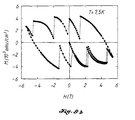
- FIG. 9 shows the magnetization hysteresis of a high transport critical current density YBa2Cu3O x sample a-b plane (H perpendicular to a-b plane) at (a) 5K, (b) 7.5 K, (c) 10 K, and (d) 20 K.
- the number of jumps was reduced from 9 to 7 at 5 K when the measuring time was doubled.
- the jumps were hardly observed for the applied field perpendicular to the sample c-axis.
- At 5 K one jump occurred at -1 T when the field sweeping back from 5.4 to -5 4 T, and no jump was observed by sweeping the field from -5.4 to 5.4 T.
- Flux jumps can be attributed to an avalanche process in the vortex line movement.
- the magnetic diffusivity is higher than the thermal diffusivity in the superconducting materials.
- the applied field was increased to some certain value or the Lorentz force was greater than the pinning force, flux lines suddenly moved and caused flux jumps. The jumps stop when the associated energy flow can be absorbed by the sample itself or its surroundings.
- Fig. 1 shows the zero-field-cooled (ZFC) magnetization data for a sample in accordance with the present invention without the steps 980 o C (48 h) and slow cooling from 980 o C to 900 o C (5 o C/h).
- Fig. 2 shows the zero-field-cooled (ZFC) magnetization data for a sample in accordance with the present invention without the steps 980 o C (48 h).
- Fig. 3 shows the zero-field-cooled (ZFC) magnetization data for a sample in accordance with all the processing steps of the present invention. It is shown that Fig. 3 has the best superconducting transition.
- Fig. 6 shows the magnetization hysteresis between -5.4 T and 5.4 T. From the Bean model, field dependent Jc was estimated up to 5 T at 77 K (as shown in Fig. 7). At zero field, Jc was found to be about 40,000 A/cm2.
- Fig. 8 shows the relationship between the voltage and the current for the silver plate used as a sample substrate.
- a preferentially-oriented bulk YBa2Cu3O x superconductor was prepared. A continuous dc current carrying capacity exceeding 120 A with critical current density, Jc, higher than 37,300 A/cm2 at 77K has been obtained.
Landscapes
- Engineering & Computer Science (AREA)
- Chemical & Material Sciences (AREA)
- Manufacturing & Machinery (AREA)
- Ceramic Engineering (AREA)
- Materials Engineering (AREA)
- Structural Engineering (AREA)
- Organic Chemistry (AREA)
- Inorganic Chemistry (AREA)
- Inorganic Compounds Of Heavy Metals (AREA)
- Superconductor Devices And Manufacturing Methods Thereof (AREA)
Abstract
Description
- The present invention relates to a preparation method of a YBa₂Cu₃Ox superconductor, wherein x = 7 - , having high transport critical current (Ic) and critical current density (Jc), obtained by a modified melt-textured growth method. In accordance with the present invention, the YBa₂Cu₃Ox superconductor formed possesses high transport Ic and Jc.
- The discovery of high critical temperature superconducting oxides, including a number of materials which superconduct above liquid-nitrogen temperature, has stimulated considerable interest and activity. A limit to applications of these materials is the low critical current density Jc measured in bulk polycrystalline samples. Several fabrication techniques to increase transport Jc have been reported in the conventional literature. Magnetic field alignment, melt-textured growth, and liquid phase methods can significantly enhance Jc values. Currently, further fabrication techniques for the preparation of YBa₂CU₃Ox superconductors and the products thereof have been proposed. However, if these superconductors are to be practically useful, the transport critical current density should be greater than 10,000 A/cm² at liquid nitrogen temperature (77K). These YBa₂Cu₃Ox superconductors obtained from general methods possess a transport critical current density from 150 to 600 A/cm² at 77 K. However, these values are far below the applicable range. The transport critical current density of a single crystal may be greater than 10⁴ A/cm², but the size of the product is small, which cannot be used in practice. The transport critical current density of epitaxially grown thin films may be greater than 10⁶ A/cm², but the film is thin, and the critical current (Ic) can only reach a maximum of about 3 to 5 amp (A). Besides, the thin film must be deposited onto an expensive single crystal substrate. Thus, the application of the product obtained in accordance with the prior process is not so convenient.
- Therefore, it is an object of the present invention to provide a method of bulk YBa₂Cu₃Ox superconductor preparation of which the superconductor can carry higher than 120 A continuous dc current, corresponding to a critical current density Jc above 37300 A/cm², at 77K. It is another object of the present invention to provide a method of bulk YBa₂Cu₃Ox superconductor preparation of which the superconductor presents a flux jump in the sample a-b plane and c-axis at low temperature.
- These and other objects, advantages and features of the present invention will be more fully understood and appreciated by reference to the written specification.
-
- Fig. 1 shows the zero-field-cooled magnetization curve of the superconductor without the steps of 980oC (48 h) and slow cooling from 980oC to 900oC (5oC/h);
- Fig. 2 shows the zero-field-cooled magnetization curve of the superconductor without the steps of annealing at 980 oC (48 h) but with furnace cooling from 980oC to 900oC in about 2 h;
- Fig. 3 shows the magnetisation curve of the superconductor obtained in accordance with the present invention;
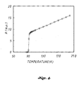
- Fig. 4 shows the relationship between the resistance and temperature of the superconductor obtained in accordance with the present method;
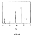
- Fig. 5 shows the X-ray diffraction pattern or the superconductor sample in accordance with the present invention;
- Fig. 6 shows the magnetization hysteresis loop of the superconductor at 77K;
- Fig. 7 shows the critical current density Jc, at 77K, calculated by Bean Model. The average grain size of the superconductor is approximately 1.5 mm;
- Fig. 8 shows the relationship between the voltage and the current of the silver plate used as a sample substrate; and
- Fig. 9 shows the magnetization hysteresis of a high transport critical current density YBa₂Cu₃Ox sample at (a) 5K, (b) 7.5 K, (c) 10 K, and (d) 20 K.
- The present invention relates to a YBa₂Cu₃Ox superconductor, wherein x = 7 - δ , having high transport current density, obtained by a modified melt-textured growth method.
- In accordance with the present invention, Y₂O₃ BaO₂, and CuO powders are uniformly mixed in a ratio of Y:Ba:Cu = 1:2:3 and pressed into a thick pellet of 2.54 cm in diameter and 0.5 to 0.8 cm thick. The thick pellet is sintered at 940oC for 24 h, reground and pressed and then annealed at 980oC for 48 h. The temperature of the sample is lowered from 980oC to 550oC in 8h and is maintained at this temperature from about 10 to 20 h. After that, the temperature is lowered to 400 oC in 8 h, maintained at 400 oC for 10 to 20 h, and finally lowered to room temperature in 6 h. At this stage, the volume of the sample is reduced by about 30% of the original volume. The sample is then introduced vertically into a furnace which is preheated to 1100oC and then annealed according to the following temperatures and time durations: 1100oC for 10 min; 1100oC to 1030oC in 20 min; 1030oC to 980oC in 50 h; 980oC for 8h; 980oC to 900oC in 16 to 30 h; 900oC to 550oC in 6 h; 500oC for 10 to 20 h; 550oC to 400 oC in 8 h; 400oC for 10 to 20 h and then to room temperature. The annealed sample in accordance with the present invention can be made into plate-shaped bulk of 8 to 10 mm in length, 5 to 6 mm in width and, 1 to 2 mm in thickness.
- Silver paint contacts are then painted on the top surface of the sample to form 4 contact points. The 4 contact points mentioned above are sintered at the following sintering temperatures and time durations. The resistivity of these contacts at 77K is 1 x 10⁻⁷ ohm cm².

- Four leads are attached to the four contact points. The resistivity of these contacts is as low as approximately 10⁻⁷ ohm cm. Then, measurements for critical current and critical current density are formed.
- The following Example further illustrates the method of preparation of the present invention. The Example is not intended to be limiting to the scope of the invention in any respect and should not be so construed.
- Bulk YBaCuOx materials and five test samples were made according to the process of this invention described above. a four terminal technique, using a dc power supply of 120A rating (H.P. 6031A) and a Keithley 181 nanometer, was employed to determine the transport Jc in the 1 uV/cm criterion.

- Table 1 lists the critical current (Ic), cross sectional area (Area), and critical current density (Jc) of the five tested samples. Samples 1 to 4 were glued onto a plastic plate by a double-sided sticker. It was observed that all the four samples burnt out. Samples 1, and 3 fractured into two parts, and
sample A. Sample 5 was attached to a silver plate (9.5 x 7.5 x 0.25 mm) by silver paint. This sample was able to sustain up to 120 A continuous dc current for 10 min without causing Voltage drop across the sample within 1 uV/cm criterion at 77K. The corresponding critical current density Jc was higher than 37300 A/cm². - The burning out and fracture of the samples may be due to the effect of contact heating. At high current, I > 70 A, the contact heating would raise the temperatures of the samples and sample substrates. In the plastic based samples, contact heating cannot be diffused into liquid nitrogen easily and continuously heated up the sample until the flux moved. The sample was then burnt out abruptly. Silver has much better thermal conductivity than plastic. Therefore, the sample attached to the silver plate could carry current up to 120 A without damaging the superconductivity. Flux jumps were observed in the magnetization hysteresis measurements for the above samples. These magnetisation jumps are similar to those found in a YBa₂Cu₃Ox single crystal prepared by conventional method. A plate type bulk YBa₂Cu₃Ox sample of dimension 4 x 3.2 x 0.5 mm with the mass of 40 mg was used in the experiment. The data was measured by a quantum designed SQUID magnetometer in the applied field (H) between -5.4 and 5.4 Tesla(T). The hysteresis loop was taken in 70 min., with one data measurement per 18 sec.. In accordance with the present invention, Fig. 9 shows the magnetization hysteresis of a high transport critical current density YBa₂Cu₃Ox sample a-b plane (H perpendicular to a-b plane) at (a) 5K, (b) 7.5 K, (c) 10 K, and (d) 20 K. At 5 K, flux jumps were observed all along the hysteresis loop (Fig. 9a). The spacing of the jumps becomes smaller when the applied field becomes bigger. At 7.5 K, the jumps are more spaced than at 5 K (Fig. 9b). There is only one jump appeared at 10 K (Fig. 9c), and no flux jump was observed at 20 K (Fig. 9d). The amplitude of magnetization seems not to change from 5 to 10 K, but significantly decreases by a factor of two at 20 K. By comparing the magnetization amplitude of the sample a-b plane at 5 and 77 K, it was estimated that the critical current density Jc is around 3 x 10⁶ A/cm² at 5 K. Flux jumps also depend on the field sweeping rate. The number of jumps was reduced from 9 to 7 at 5 K when the measuring time was doubled. The jumps were hardly observed for the applied field perpendicular to the sample c-axis. At 5 K one jump occurred at -1 T when the field sweeping back from 5.4 to -5 4 T, and no jump was observed by sweeping the field from -5.4 to 5.4 T.
- Flux jumps can be attributed to an avalanche process in the vortex line movement. At low temperatures, the magnetic diffusivity is higher than the thermal diffusivity in the superconducting materials. In other words, as the applied field was increased to some certain value or the Lorentz force was greater than the pinning force, flux lines suddenly moved and caused flux jumps. The jumps stop when the associated energy flow can be absorbed by the sample itself or its surroundings.
- The application of high Tc superconductors is strongly dependent on their critical current density Jc. To increase Jc, the spinning force in the sample must be increased. But due to the low thermal conductivity of these materials, pinning force is not the only factor which affects the current density. The magnetic and thermal properties of the sample and its surroundings need to be considered as well.
- The degree of sample orientation was determined from x-ray reflection spectra. The reflectivity is from the broad face of the sample, perpendicular to the c-axis in an oriented sample, so that in a perfectly oriented sample only (001)-reflections would contribute to X-ray reflection. Fig. 4 shows the relationship between the resistance and temperature of the superconductor obtained in accordance with the present method. Fig. 5 shows the X-ray reflection of a rectangle sample with dimensions of approximately 6x5x1 mm.
- The magnetization and hysteresis data were measured by a quantum designed SQUID magnetometer. The three annealing procedures studied resulted in different magnetization data. Fig. 1 shows the zero-field-cooled (ZFC) magnetization data for a sample in accordance with the present invention without the steps 980oC (48 h) and slow cooling from 980oC to 900oC (5oC/h). Fig. 2 shows the zero-field-cooled (ZFC) magnetization data for a sample in accordance with the present invention without the steps 980oC (48 h). Fig. 3 shows the zero-field-cooled (ZFC) magnetization data for a sample in accordance with all the processing steps of the present invention. It is shown that Fig. 3 has the best superconducting transition.
- The anisotropic properties of magnetization for an applied field parallel and perpendicular to the sample a-b plane were studied. Eliminating the geometric factor, the magnetization of a-b plane is isotropic for ZFC, and the FC had an anisotropic property, whose ratio was 4:3.
- Fig. 6 shows the magnetization hysteresis between -5.4 T and 5.4 T. From the Bean model, field dependent Jc was estimated up to 5 T at 77 K (as shown in Fig. 7). At zero field, Jc was found to be about 40,000 A/cm². Fig. 8 shows the relationship between the voltage and the current for the silver plate used as a sample substrate. In accordance with the present invention, a preferentially-oriented bulk YBa₂Cu₃Ox superconductor was prepared. A continuous dc current carrying capacity exceeding 120 A with critical current density, Jc, higher than 37,300 A/cm² at 77K has been obtained.
- The invention has been described in detail including the preferred embodiment thereof. However, it will be appreciated that those skilled in the art, upon consideration of this disclosure, may make modifications and improvements within the spirit and scope of this invention.
Claims (2)
- A preparation method of bulk YBa₂Cu₃Ox superconductors with high transport critical current and critical current density, wherein x is 7 - δ , comprising the steps of :(l) mixing Y₂O₃, BaO₂ and CuO in a ratio of Y:Ba:Cu = 1:2:3 and compressing the mixture into a pellet of diameter 2.54 cm and a thickness of 0.5 to 0.8 cm;(ll) annealing said pellet at a temperature of 940oC for 24 h and then lowering to room temperature;(lll) grinding said pellet to fine powder and then compressing to form a new pellet;(lV) annealing the pellet obtained from (lll) in a furnace at a temperature of 980oC for 48 h to 72 h;(V) lowering the temperature of said pellet to 550oC and maintaining at this temperature for 10 h to 20 h, and then lowering the temperature to 400oC in 8 h and maintaining at this temperature for 10 h to 20 h, and lowering to room temperature;(Vl) introducing said pellet into a furnace preheated to 1100oC and maintaining at this temperature for 10 mins, lowering the temperature from 1100oC to 1030oC in 20 min, 1030oC to 980 oC in 50 h; and(Vll) maintaining the temperature of said pellet at 980oC for 8 h, lowering the temperature from 980 to 900oC in 16 to 30 h, lowering the temperature to 550oC in 6 h, maintaining at 550oC for 10 to 20 h, lowering the temperature from 550oC to 400oC in 8 h. maintaining the temperature at 400oC for 10 to 20 h and lowering the temperature of said pellet to room temperature.
- A preparation method of bulk YBa₂Cu₃Ox superconductors with high transport critical current and critical current density as set forth in Claim 1, wherein the pellet in (lV) is annealed in a furnace for 48 h in flowing oxygen.
Priority Applications (3)
| Application Number | Priority Date | Filing Date | Title |
|---|---|---|---|
| DE90108127T DE69006351T2 (en) | 1990-04-27 | 1990-04-27 | Process for the production of the Y-Ba-Cu-O superconductor in bulk with high, critical current density. |
| EP90108127A EP0453615B1 (en) | 1990-04-27 | 1990-04-27 | A preparation method of bulk Y-Ba-Cu-O superconductors with high transport critical current density |
| US07/516,058 US5077272A (en) | 1990-04-27 | 1990-04-27 | Preparation method of bulk Y--Ba--Cu--O superconductors with high transport critical current density |
Applications Claiming Priority (1)
| Application Number | Priority Date | Filing Date | Title |
|---|---|---|---|
| EP90108127A EP0453615B1 (en) | 1990-04-27 | 1990-04-27 | A preparation method of bulk Y-Ba-Cu-O superconductors with high transport critical current density |
Publications (2)
| Publication Number | Publication Date |
|---|---|
| EP0453615A1 true EP0453615A1 (en) | 1991-10-30 |
| EP0453615B1 EP0453615B1 (en) | 1994-01-26 |
Family
ID=8203930
Family Applications (1)
| Application Number | Title | Priority Date | Filing Date |
|---|---|---|---|
| EP90108127A Expired - Lifetime EP0453615B1 (en) | 1990-04-27 | 1990-04-27 | A preparation method of bulk Y-Ba-Cu-O superconductors with high transport critical current density |
Country Status (3)
| Country | Link |
|---|---|
| US (1) | US5077272A (en) |
| EP (1) | EP0453615B1 (en) |
| DE (1) | DE69006351T2 (en) |
Families Citing this family (7)
| Publication number | Priority date | Publication date | Assignee | Title |
|---|---|---|---|---|
| US5278137A (en) * | 1988-06-06 | 1994-01-11 | Nippon Steel Corporation | YBa2 Cu3 O7-y type oxide superconductive material containing dispersed Y2 BaCuO5 phase and having high critical current density |
| US5306697A (en) * | 1989-02-10 | 1994-04-26 | University Of Houston - University Park | Oriented grained Y-Ba-Cu-O superconductors having high critical currents and method for producing same |
| US5340794A (en) * | 1989-08-02 | 1994-08-23 | Her Majesty The Queen In Right Of New Zealand | Flux pinning in superconducting cuprates |
| USRE37587E1 (en) * | 1990-12-28 | 2002-03-19 | Sumitomo Electric Industries Ltd. | Superconducting quantum interference device formed of oxide superconductor thin film |
| US5612545A (en) * | 1991-12-23 | 1997-03-18 | Sumitomo Electric Industries, Ltd. | Superconducting quantum interference device formed of oxide superconductor thin film |
| KR0166465B1 (en) * | 1995-11-03 | 1999-01-15 | 한승준 | Preparation of catalyst for cleaning exhaust gases |
| US20080146449A1 (en) * | 2006-12-14 | 2008-06-19 | Jerome Lesueur | Electrical device and method of manufacturing same |
Citations (3)
| Publication number | Priority date | Publication date | Assignee | Title |
|---|---|---|---|---|
| DE3913397A1 (en) * | 1989-04-24 | 1989-10-19 | Asea Brown Boveri | METHOD FOR PRODUCING A HIGH TEMPERATURE SUPER LADDER |
| EP0351844A2 (en) * | 1988-07-20 | 1990-01-24 | The Furukawa Electric Co., Ltd. | Method of manufacturing bismuth type oxide superconductor |
| EP0358530A2 (en) * | 1988-09-09 | 1990-03-14 | The Dow Chemical Company | Novel method for producing ceramic bodies |
Family Cites Families (2)
| Publication number | Priority date | Publication date | Assignee | Title |
|---|---|---|---|---|
| US4943557A (en) * | 1988-08-15 | 1990-07-24 | At&T Bell Laboratories | Method of making a high density YBa Cu3 Ox superconductor material |
| US4956336A (en) * | 1989-02-10 | 1990-09-11 | University Of Houston - University Park | Oriented grained Y-Ba-Cu-O superconductors having high critical currents and method for producing same |
-
1990
- 1990-04-27 EP EP90108127A patent/EP0453615B1/en not_active Expired - Lifetime
- 1990-04-27 DE DE90108127T patent/DE69006351T2/en not_active Expired - Fee Related
- 1990-04-27 US US07/516,058 patent/US5077272A/en not_active Expired - Fee Related
Patent Citations (3)
| Publication number | Priority date | Publication date | Assignee | Title |
|---|---|---|---|---|
| EP0351844A2 (en) * | 1988-07-20 | 1990-01-24 | The Furukawa Electric Co., Ltd. | Method of manufacturing bismuth type oxide superconductor |
| EP0358530A2 (en) * | 1988-09-09 | 1990-03-14 | The Dow Chemical Company | Novel method for producing ceramic bodies |
| DE3913397A1 (en) * | 1989-04-24 | 1989-10-19 | Asea Brown Boveri | METHOD FOR PRODUCING A HIGH TEMPERATURE SUPER LADDER |
Non-Patent Citations (1)
| Title |
|---|
| CHEMICAL ABSTRACTS, vol. 109, no. 10, 05 September 1988 Columbus, Ohio, USA Z.Pan et al.: "Refractories for induction-furnace bodies,and baking of the refractories" page 331; ref. no. 78605Q * |
Also Published As
| Publication number | Publication date |
|---|---|
| EP0453615B1 (en) | 1994-01-26 |
| US5077272A (en) | 1991-12-31 |
| DE69006351T2 (en) | 1994-05-11 |
| DE69006351D1 (en) | 1994-03-10 |
Similar Documents
| Publication | Publication Date | Title |
|---|---|---|
| Cava et al. | Bulk superconductivity at 36 K in La 1.8 Sr 0.2 CuO 4 | |
| Yang et al. | High temperature superconductivity in rare-earth (R)-barium copper oxides (RBa2) Cu3O9− σ | |
| Ekin et al. | Double-step behavior of critical current vs. magnetic field in Y-, Bi-and Tl-based bulk high-Tc superconductors | |
| Jung et al. | Flux motion, proximity effect, and critical current density in YBa 2 Cu 3 O 7− δ/silver composites | |
| Beille et al. | Superconductivity of La2CuxO4− y | |
| Junod et al. | Structure, resistivity, critical field, specific-Heat jump at Tc, meissner effect, ac and dc susceptibility of the high-Tc superconductor YBa2Cu3O7 | |
| Chen et al. | High transport critical currents and flux jumps in bulk YBa2Cu3O x superconductors | |
| EP0453615B1 (en) | A preparation method of bulk Y-Ba-Cu-O superconductors with high transport critical current density | |
| Fang et al. | Fabrication of Y123 disk by the seeded infiltration and growth method | |
| Polak et al. | Critical current density, magnetization and AC losses in the YBa2Cu3O6. 5+ x superconductor | |
| Chu et al. | Grain growth and the microstructural effects on the properties of YBa2Cu3O7− y superconductor | |
| Ou et al. | Superconducting thin films of (Cu, C) Ba2Ca2Cu3O9±δ with zero-resistance transition temperature close to 100 K | |
| Nariki et al. | Peak effect in field trapping properties of large grain Dy–Ba–Cu–O/Ag bulk superconductors | |
| Hsu et al. | Temperature and field-sweeping rate dependence of flux jumps in a melt-textured YBa2Cu3O7− x superconductor | |
| Leiderer et al. | Tunneling and point contact investigations of La 1.85 Sr 0.15 CuO 4 | |
| Peng et al. | The preparation of Tl-1223 superconductors and Ag-sheathed tapes | |
| US5053385A (en) | Preferential orientation of metal oxide superconducting materials | |
| Symko et al. | Dissipative flow of Josephson and Abrikosov fluxons in high Tc superconductors | |
| Gerber et al. | Granular Superconductivity in the Electron-Doped Compounds Ln2-xMxCuO4-y (Ln= Pr, Nd, Sm, Eu; M= Ce, Th) | |
| Bai et al. | Melt-textured YBa/sub 2/Cu/sub 3/O/sub 7/for low-field applications in microwave devices | |
| JPH0764629B2 (en) | Manufacturing method of bulk Y-Ba-Cu-O superconductor having high transport limiting current density | |
| Sekula et al. | Superconductivity, critical current density, and magnetic properties of Fe-substituted Y/sub 1/Ba/sub 2/(Cu/sub 1-x/Fe/sub x/)/sub 3/O/sub z/materials | |
| Hascicek et al. | Anomalous behavior in transport critical current density of YBa2Cu3O7− x and YBa2Cu3O7− x‐Ag bulk samples | |
| Paterno et al. | DC critical currents in superconducting ceramic samples of Y/sub 1/Ba/sub 2/Cu/sub 3/O/sub 7 | |
| Zannella et al. | Magnetic properties of BiSrCaCu2Ox high-temperature superconductor |
Legal Events
| Date | Code | Title | Description |
|---|---|---|---|
| PUAI | Public reference made under article 153(3) epc to a published international application that has entered the european phase |
Free format text: ORIGINAL CODE: 0009012 |
|
| AK | Designated contracting states |
Kind code of ref document: A1 Designated state(s): DE FR GB |
|
| 17P | Request for examination filed |
Effective date: 19920213 |
|
| 17Q | First examination report despatched |
Effective date: 19920515 |
|
| GRAA | (expected) grant |
Free format text: ORIGINAL CODE: 0009210 |
|
| AK | Designated contracting states |
Kind code of ref document: B1 Designated state(s): DE FR GB |
|
| REF | Corresponds to: |
Ref document number: 69006351 Country of ref document: DE Date of ref document: 19940310 |
|
| ET | Fr: translation filed | ||
| PLBE | No opposition filed within time limit |
Free format text: ORIGINAL CODE: 0009261 |
|
| STAA | Information on the status of an ep patent application or granted ep patent |
Free format text: STATUS: NO OPPOSITION FILED WITHIN TIME LIMIT |
|
| 26N | No opposition filed | ||
| REG | Reference to a national code |
Ref country code: GB Ref legal event code: IF02 |
|
| PGFP | Annual fee paid to national office [announced via postgrant information from national office to epo] |
Ref country code: GB Payment date: 20020415 Year of fee payment: 13 |
|
| PGFP | Annual fee paid to national office [announced via postgrant information from national office to epo] |
Ref country code: FR Payment date: 20020416 Year of fee payment: 13 |
|
| PGFP | Annual fee paid to national office [announced via postgrant information from national office to epo] |
Ref country code: DE Payment date: 20020529 Year of fee payment: 13 |
|
| PG25 | Lapsed in a contracting state [announced via postgrant information from national office to epo] |
Ref country code: GB Free format text: LAPSE BECAUSE OF NON-PAYMENT OF DUE FEES Effective date: 20030427 |
|
| PG25 | Lapsed in a contracting state [announced via postgrant information from national office to epo] |
Ref country code: DE Free format text: LAPSE BECAUSE OF NON-PAYMENT OF DUE FEES Effective date: 20031101 |
|
| GBPC | Gb: european patent ceased through non-payment of renewal fee | ||
| PG25 | Lapsed in a contracting state [announced via postgrant information from national office to epo] |
Ref country code: FR Free format text: LAPSE BECAUSE OF NON-PAYMENT OF DUE FEES Effective date: 20031231 |
|
| REG | Reference to a national code |
Ref country code: FR Ref legal event code: ST |