EP0452938B1 - Optical integrated circuit - Google Patents
Optical integrated circuit Download PDFInfo
- Publication number
- EP0452938B1 EP0452938B1 EP91106246A EP91106246A EP0452938B1 EP 0452938 B1 EP0452938 B1 EP 0452938B1 EP 91106246 A EP91106246 A EP 91106246A EP 91106246 A EP91106246 A EP 91106246A EP 0452938 B1 EP0452938 B1 EP 0452938B1
- Authority
- EP
- European Patent Office
- Prior art keywords
- optical
- optical waveguide
- integrated circuit
- waveguides
- waveguide
- Prior art date
- Legal status (The legal status is an assumption and is not a legal conclusion. Google has not performed a legal analysis and makes no representation as to the accuracy of the status listed.)
- Expired - Lifetime
Links
Images

Classifications
-
- G—PHYSICS
- G01—MEASURING; TESTING
- G01C—MEASURING DISTANCES, LEVELS OR BEARINGS; SURVEYING; NAVIGATION; GYROSCOPIC INSTRUMENTS; PHOTOGRAMMETRY OR VIDEOGRAMMETRY
- G01C19/00—Gyroscopes; Turn-sensitive devices using vibrating masses; Turn-sensitive devices without moving masses; Measuring angular rate using gyroscopic effects
- G01C19/58—Turn-sensitive devices without moving masses
- G01C19/64—Gyrometers using the Sagnac effect, i.e. rotation-induced shifts between counter-rotating electromagnetic beams
- G01C19/72—Gyrometers using the Sagnac effect, i.e. rotation-induced shifts between counter-rotating electromagnetic beams with counter-rotating light beams in a passive ring, e.g. fibre laser gyrometers
- G01C19/721—Details, e.g. optical or electronical details
- G01C19/722—Details, e.g. optical or electronical details of the mechanical construction
-
- G—PHYSICS
- G02—OPTICS
- G02B—OPTICAL ELEMENTS, SYSTEMS OR APPARATUS
- G02B6/00—Light guides; Structural details of arrangements comprising light guides and other optical elements, e.g. couplings
- G02B6/10—Light guides; Structural details of arrangements comprising light guides and other optical elements, e.g. couplings of the optical waveguide type
- G02B6/12—Light guides; Structural details of arrangements comprising light guides and other optical elements, e.g. couplings of the optical waveguide type of the integrated circuit kind
- G02B6/122—Basic optical elements, e.g. light-guiding paths
- G02B6/125—Bends, branchings or intersections
-
- G—PHYSICS
- G02—OPTICS
- G02B—OPTICAL ELEMENTS, SYSTEMS OR APPARATUS
- G02B6/00—Light guides; Structural details of arrangements comprising light guides and other optical elements, e.g. couplings
- G02B6/24—Coupling light guides
- G02B6/26—Optical coupling means
- G02B6/28—Optical coupling means having data bus means, i.e. plural waveguides interconnected and providing an inherently bidirectional system by mixing and splitting signals
- G02B6/2804—Optical coupling means having data bus means, i.e. plural waveguides interconnected and providing an inherently bidirectional system by mixing and splitting signals forming multipart couplers without wavelength selective elements, e.g. "T" couplers, star couplers
-
- G—PHYSICS
- G02—OPTICS
- G02B—OPTICAL ELEMENTS, SYSTEMS OR APPARATUS
- G02B6/00—Light guides; Structural details of arrangements comprising light guides and other optical elements, e.g. couplings
- G02B6/24—Coupling light guides
- G02B6/42—Coupling light guides with opto-electronic elements
-
- G—PHYSICS
- G02—OPTICS
- G02B—OPTICAL ELEMENTS, SYSTEMS OR APPARATUS
- G02B6/00—Light guides; Structural details of arrangements comprising light guides and other optical elements, e.g. couplings
- G02B6/24—Coupling light guides
- G02B6/42—Coupling light guides with opto-electronic elements
- G02B6/4201—Packages, e.g. shape, construction, internal or external details
- G02B6/4246—Bidirectionally operating package structures
Definitions
- the present invention relates to an optical integrated circuit which has branched optical waveguides, and more particularly to an optical integrated circuit which permits direct mounting thereon of a photodetector, a light emitting element, or similar optical active elements and can be miniaturized.
- Fig. 1 shows a conventional optical integrated circuit, indicated generally by 28.
- an electrooptic plate 11 as of lithium niobate (LiNbO3) there is formed an optical waveguide 12, which has its one end branched into optical waveguides 13 and 14 extending to optical waveguide terminals 15 and 16 at one side of the electrooptic plate 11 and has its other end branched into optical waveguides 17 and 18 extending to optical waveguide terminals 21 and 22 at the opposite side of the electrooptic plate 11.
- Electrodes 23 are formed on both sides of the parallel-extending portions of the optical waveguides 17 and 18 near the terminals 21 and 22 to provide an optical phase modulating function.
- Figs. 2A and 2B are a front view and a plan view of an optical fiber holder for holding two optical fibers.
- the optical fiber holder is composed of two holder halves 24 and 25, which are assembled together to fixedly hold two optical fibers 26 and 27 at one end disposed in parallel as shown and their end faces are ground or polished.
- the core spacing D2 of the optical fibers 26 and 27 is equal to the outer diameter of each optical fiber. Since the outer diameter of the optical fiber is 125 »m, for example, in the case of a single mode optical fiber commercially available in Japan, the spacing D2 is 125 »m, for instance. Accordingly, the distance D1 between optical waveguide terminals at one side of the optical integrated circuit 28 is also designed to be 125 »m.
- the angle of bend ⁇ at which the optical waveguide is branched is several degrees or less in many cases.
- the angle of bend ⁇ of the branched optical waveguide 17 to the optical waveguide 12 is, for example, 1° in Fig. 1.
- the spacing D1 may be 125 »m
- the lengths L2 of those portions of the branched optical waveguides 17 and 18 which are inclined to the optical waveguide 12 are about 3.6 mm.
- the length L3 of the optical waveguide 12 is 7 mm
- the length L5 of each of the parallel portions of the optical waveguides 17 and 18 where the optical phase modulating function is provided is 12 mm
- the length L1 of each of the parallel portions of the optical waveguides 13 and 14 is 3 mm
- the entire length L of the optical integrated circuit is 29.2 mm.
- FIG. 1 The optical integrated circuit shown in Fig. 1 is used in a fiber optic gyro, for instance.
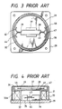
- Figs. 3 and 4 show an example of the fiber optic gyro, in which a bobbin 32 with an optical fiber coil 33 wound thereon is mounted on a chassis 29 covered with a cover 29, a light source module 34 and a photodetector module 35 are disposed inside the bobbin 32, a base plate 36 is disposed on an upper plate 32A of the bobbin 32 and the optical integrated circuit 28 is mounted on the base plate 36 through a mounting plate 37.
- Optical fiber holders 39 and 41 are fixedly bonded to the two optical waveguide terminals at the opposite sides of the optical integrated circuit 28.
- the one optical fiber 42 held by the holder 39 is connected by fusion to an optical fiber 43 extending from the light source module 34, whereas the other optical fiber 44 is connected by fusion to an optical fiber 45 extending from the photodetector module 35.
- Optical fibers 46 and 47 held by the holder 41 are each connected by fusion to one end of the optical fiber coil 33.
- the optical integrated circuit and other modules are thus connected using optical fibers.
- first and second optical waveguides formed on an electrooptic plate each extend at one end to one side of the electrooptic plate
- the other ends of the first and second optical waveguides are connected to each other and the connection point is connected to a third optical waveguide so that light beams from the first and second optical waveguides are supplied together to the third optical waveguide and light from the latter is branched to the former
- one of the first optical waveguide meets the corresponding side of the electrooptic plate at an angle which deviates from 90°
- the end face of the first optical waveguide forms a reflecting surface
- a fourth optical waveguide is provided by which light reflected by the reflecting surface is guided to another side of the electrooptic plate.
- the optical waveguide terminals are sufficiently spaced apart so that active elements such as a photodetector and a light emitting element can be mounted directly on the optical integrated circuit.
- Fig. 5 illustrates an embodiment of the present invention, in which the parts corresponding to those in Fig. 1 are identified by the same reference numerals.
- the terminal portion of the optical waveguide 14 meets one side 11a of the electrooptic plate 11 at an angle which deviates from 90°; namely, the optical waveguide terminal 16 of the optical waveguide 14 is inclined by an angle ⁇ 1 to a line 48 which is perpendicular to the one side 11a of the electrooptic plate 11.
- the end face of the optical waveguide 14 and consequently the end face of the optical waveguide terminal 16 forms a reflecting surface 49, which is coated with a reflecting film 54 to ensure the reflection by the reflecting surface 49.
- the reflecting film 54 can easily be coated by the evaporation of aluminum.
- an optical waveguide 51 by which light reflected by the reflecting surface 49 is guided to another side 11b of the electrooptic plate 11.
- a photodetector 53 which is a photoelectric transducer in this example.
- the angle between the side 11a of the electrooptic plate 11 and the optical waveguides 13 and 14 is deviated by ⁇ 2 from a right angle and the angle of the side 11c of the electrooptic plate 11 and the optical waveguides 17 and 18 is deviated by ⁇ 3 from a right angle so as to preclude the possibility of the occurrence of a Fresnel reflection on the end faces of the optical waveguides and hence prevent the occurrence of return light.
- the angles ⁇ 2 and ⁇ 3 each differ with the refractive index of the optical active element that is connected to the optical waveguide terminal.
- the optical integrated circuit 55 of this embodiment is of about the same size as that of the conventional integrated circuit shown in Fig. 1, if the optical fiber 125 »m in diameter is used, that is, if the distance D1 is 125 »m.
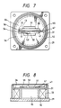
- Figs. 6 through 8 illustrates, by way of example, the case where the optical integrated circuit 55 depicted in Fig. 5 is built in a fiber optic gyro.
- a light emitting element 56 is fixed directly to the terminal 15 of the optical integrated circuit 55 as shown in Fig. 6.
- the light emitting element 56 is driven by a light source driver 57 and the resulting light reaches the optical waveguide 12 via the optical waveguide 13.
- the light having reached the optical waveguide 12 is split to light beams which are guided the optical waveguides 17 and 18, from which they propagated through the optical fiber coil 33 in opposite directions.
- the light beams having thus propagated through the optical fiber coil 33 are coupled together by the optical waveguide 12 to form interference light.
- the interference light is branched to the optical waveguides 13 and 14 and the light branched to the optical waveguide 14 is reflected by the reflecting film 54 to the photodetector 53 via the optical waveguide 51.
- a signal resulting from the photoelectric conversion by the photodetector 53 is amplified by an amplifier 58 and is then applied to a signal processor 59 formed by a synchronous detector.
- the input signal is processed by the signal processor 59 and is provided therefrom as the gyro output to a terminal 61.
- a phase modulator 62 formed on the optical waveguide 18 of the optical integrated circuit 55 is provided for accurately detecting input angular rate information which is provided to the optical fiber coil 33.
- a phase modulating voltage from a phase modulator driver 63 is applied across the electrodes of the phase modulator 62.
- the optical fibers 46 and 47 connected to the optical integrated circuit 55 by means of the holder 41 are each fused to one end of the optical fiber coil 33.
- the light emitting element 56 is connected to the optical waveguide terminal 15 of the optical waveguide 13. It is also possible, in this case, to form an optical waveguide type lens (such as a mode index lens, geodesic lens, or grating lens) near the optical waveguide terminal 15 of the optical waveguide 13 so as to improve the coupling between the light emitting element 56 and the optical waveguide 13.
- the photodetector 53 is bonded to the optical waveguide terminal 52 of the optical waveguide 51.
- the ceramic base plate 36 as of ceramics, on which there are mounted the optical integrated circuit 55 and a hybrid IC carrying the light source driver 57, the amplifier 58, the phase modulator driver 63, etc. shown in Fig. 6.
- a space 65 inside of the bobbin 32 there are disposed the photodetector module and the light source module in the prior art example depicted in Figs. 3 and 4, but in this embodiment the photodetector 53 and the light emitting element 56 are mounted on the optical integrated circuit 55, and consequently the signal processor 59 and others can be housed in the empty space.
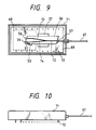
- Figs. 9 and 10 illustrates an example of another embodiment of the present invention as applied to a transmitter-receiver module.
- An optical integrated circuit 66 is formed by the optical waveguides 12, 13, 14 and 51 of the optical integrated circuit 55 shown in Fig. 5.
- Light from the light emitting element 56 passes through the optical waveguide 13 and enters into the optical waveguide 12, from which it is provided on an optical fiber 67 for transmission.
- light transmitted over the optical fiber 67 enters into the optical waveguide 12, from which it is branched to the optical waveguides 13 and 14.
- the light branched to the optical waveguide 14 is reflected by the reflecting film 54 to the photodetector 53 via the optical waveguide 51.
- a space 68 indicated by the broken line there are disposed on a base plate 69 as of ceramics, together with the optical integrated circuit 66, an electronic circuit for driving the light emitting element 56 and a circuit for amplifying the output signal from the photodetector 53, the both circuits being miniaturized through use of hybrid IC packaging techniques.
- the circuits mounted on the base plate 69 are hermetically sealed by a cover case 71 and each terminal 72 is a hermetic terminal.
- the optical waveguide 51 may also be formed so that its terminal 52 extends to the side 11c of the electrooptic plate 11. Also in such a case, the terminal 52 and those 21 and 22 can be spaced a large distance apart. The terminal 52 may also be extended to another side 11d of the electrooptic plate 11. In this instance, the optical waveguide 51 crosses other optical waveguides, but this can be implemented by sufficiently reducing its coupling with the crossed optical waveguides.
- the reflecting surface may also be formed on the end face of the optical waveguide 13 in place of the end face of the optical waveguide 14 and its terminal may be guided to another side of the electrooptic plate 11. Similarly, one terminal of each of the optical waveguides 17 and 18 may be positioned at another side of the plate 11.
- a photodetector, light emitting element or optical fiber can be connected directly to an optical integrated circuit with branched optical waveguides by employing a structure in which light in one of the branched optical waveguide is reflected by an end face of the optical integrated circuit to another end face thereof.
- the optical integrated circuit can be made small. This permits miniaturization of devices using the miniaturized optical integrated circuit, such as a fiber optic gyro and a transmitter-receiver module.
Landscapes
- Physics & Mathematics (AREA)
- Optics & Photonics (AREA)
- General Physics & Mathematics (AREA)
- Engineering & Computer Science (AREA)
- Electromagnetism (AREA)
- Power Engineering (AREA)
- Radar, Positioning & Navigation (AREA)
- Remote Sensing (AREA)
- Microelectronics & Electronic Packaging (AREA)
- Optical Integrated Circuits (AREA)
- Optical Couplings Of Light Guides (AREA)
- Gyroscopes (AREA)
Description
- The present invention relates to an optical integrated circuit which has branched optical waveguides, and more particularly to an optical integrated circuit which permits direct mounting thereon of a photodetector, a light emitting element, or similar optical active elements and can be miniaturized.
- Fig. 1 shows a conventional optical integrated circuit, indicated generally by 28. On an
electrooptic plate 11 as of lithium niobate (LiNbO₃) there is formed anoptical waveguide 12, which has its one end branched intooptical waveguides optical waveguide terminals electrooptic plate 11 and has its other end branched intooptical waveguides optical waveguide terminals electrooptic plate 11. Electrodes 23 are formed on both sides of the parallel-extending portions of theoptical waveguides terminals - For input and output of light with respect to such an optical integrated circuit, it is a common practice in the prior art to employ a method in which an optical fiber has its one end face fixedly bonded to each optical waveguide terminal, or a method in which optical fibers of the same number as that of the optical waveguide terminals at one side of the
electrooptic plate 11 are fixed to an optical fiber holder which is connected to the optical integrated circuit. - Figs. 2A and 2B are a front view and a plan view of an optical fiber holder for holding two optical fibers. The optical fiber holder is composed of two holder halves 24 and 25, which are assembled together to fixedly hold two optical fibers 26 and 27 at one end disposed in parallel as shown and their end faces are ground or polished. The core spacing D₂ of the optical fibers 26 and 27 is equal to the outer diameter of each optical fiber. Since the outer diameter of the optical fiber is 125 »m, for example, in the case of a single mode optical fiber commercially available in Japan, the spacing D₂ is 125 »m, for instance. Accordingly, the distance D₁ between optical waveguide terminals at one side of the optical integrated
circuit 28 is also designed to be 125 »m. - The angle of bend ϑ at which the optical waveguide is branched is several degrees or less in many cases. Now, consider that the angle of bend ϑ of the branched
optical waveguide 17 to theoptical waveguide 12 is, for example, 1° in Fig. 1. In order that the spacing D₁ may be 125 »m, the lengths L₂ of those portions of the branchedoptical waveguides optical waveguide 12 are about 3.6 mm. In the case where the length L₃ of theoptical waveguide 12 is 7 mm, the length L₅ of each of the parallel portions of theoptical waveguides optical waveguides - The optical integrated circuit shown in Fig. 1 is used in a fiber optic gyro, for instance. Figs. 3 and 4 show an example of the fiber optic gyro, in which a
bobbin 32 with anoptical fiber coil 33 wound thereon is mounted on achassis 29 covered with acover 29, alight source module 34 and aphotodetector module 35 are disposed inside thebobbin 32, abase plate 36 is disposed on anupper plate 32A of thebobbin 32 and the optical integratedcircuit 28 is mounted on thebase plate 36 through amounting plate 37. -
Optical fiber holders circuit 28. The oneoptical fiber 42 held by theholder 39 is connected by fusion to anoptical fiber 43 extending from thelight source module 34, whereas the otheroptical fiber 44 is connected by fusion to anoptical fiber 45 extending from thephotodetector module 35.Optical fibers holder 41 are each connected by fusion to one end of theoptical fiber coil 33. Conventionally, the optical integrated circuit and other modules are thus connected using optical fibers. - In the optical
integrated circuit 28 depicted in Fig. 1, since the distance D₁ between two optical waveguide terminals is only 125 »m or so, a photodetector and a light emitting element, or an optical fiber holder and a photodetector or light emitting element, each having a 1 mm or more chip size, cannot be mounted side by side on the optical integratedcircuit 28. To mount the photodetector and the light emitting element side by side on the optical integrated circuit, it is necessary to increase the distance D₁ between the optical waveguide terminals, and this calls for an increase in the length L₂ of each of the inclined portions of the branchedoptical waveguides - It is therefore an object of the present invention to provide a miniature optical integrated circuit in which optical waveguide terminals are sufficiently spaced apart to permit direct mounting thereon of a photodetector and a light emitting element.
- This object is achieved with an optical integrated circuit as claimed in claim 1.
- Specific embodiments of the invention are subject-matter of the dependent claims.
- According to the present invention, in the optical integrated circuit wherein first and second optical waveguides formed on an electrooptic plate each extend at one end to one side of the electrooptic plate, the other ends of the first and second optical waveguides are connected to each other and the connection point is connected to a third optical waveguide so that light beams from the first and second optical waveguides are supplied together to the third optical waveguide and light from the latter is branched to the former, one of the first optical waveguide meets the corresponding side of the electrooptic plate at an angle which deviates from 90°, the end face of the first optical waveguide forms a reflecting surface and a fourth optical waveguide is provided by which light reflected by the reflecting surface is guided to another side of the electrooptic plate.
- With such a structure as mentioned above, even if the branched optical waveguides are formed short, that is, even if the optical integrated circuit is formed small, the optical waveguide terminals are sufficiently spaced apart so that active elements such as a photodetector and a light emitting element can be mounted directly on the optical integrated circuit.
-
- Fig. 1 is a plan view showing a conventional optical integrated circuit;
- Fig. 2A is a front view of an optical fiber holder;
- Fig. 2B is a top plan view of the optical fiber holder;
- Fig. 3 is a plan view showing the construction of a conventional fiber optic gyro;
- Fig. 4 is its sectional view;
- Fig. 5 is a diagram schematically illustrating an embodiment of the present invention;
- Fig. 6 is a block diagram showing the functional configuration of the fiber optic gyro utilizing the optical integrated circuit depicted in Fig. 5;
- Fig. 7 is a plan view illustrating an example of the construction of the fiber optic gyro shown in Fig. 6;
- Fig. 8 is a side view of the fiber optic gyro shown in Fig. 7;
- Fig. 9 is a plan view illustrating a transmitting-receiving module utilizing the optical integrated circuit of the present invention; and
- Fig. 10 is a front view of the module shown in Fig. 9.
- Fig. 5 illustrates an embodiment of the present invention, in which the parts corresponding to those in Fig. 1 are identified by the same reference numerals. In this embodiment the terminal portion of the
optical waveguide 14 meets oneside 11a of theelectrooptic plate 11 at an angle which deviates from 90°; namely, theoptical waveguide terminal 16 of theoptical waveguide 14 is inclined by an angle ϑ₁ to aline 48 which is perpendicular to the oneside 11a of theelectrooptic plate 11. The end face of theoptical waveguide 14 and consequently the end face of theoptical waveguide terminal 16 forms a reflectingsurface 49, which is coated with a reflectingfilm 54 to ensure the reflection by thereflecting surface 49. The reflectingfilm 54 can easily be coated by the evaporation of aluminum. In this embodiment there is formed anoptical waveguide 51 by which light reflected by the reflectingsurface 49 is guided to anotherside 11b of theelectrooptic plate 11. To that end of theoptical waveguide 51 which meets theside 11b of theelectrooptic plate 11, that is, to an optical waveguide terminal, there is fixedly bonded aphotodetector 53 which is a photoelectric transducer in this example. - In the Fig. 5 embodiment the angle between the
side 11a of theelectrooptic plate 11 and theoptical waveguides side 11c of theelectrooptic plate 11 and theoptical waveguides optical waveguide 14 and theside 11a is deviated from a right angle through utilization of the angle ϑ₂, and hence
- The optical
integrated circuit 55 of this embodiment is of about the same size as that of the conventional integrated circuit shown in Fig. 1, if the optical fiber 125 »m in diameter is used, that is, if the distance D₁ is 125 »m. - Figs. 6 through 8 illustrates, by way of example, the case where the optical
integrated circuit 55 depicted in Fig. 5 is built in a fiber optic gyro. At first, alight emitting element 56 is fixed directly to theterminal 15 of the opticalintegrated circuit 55 as shown in Fig. 6. Thelight emitting element 56 is driven by alight source driver 57 and the resulting light reaches theoptical waveguide 12 via theoptical waveguide 13. The light having reached theoptical waveguide 12 is split to light beams which are guided theoptical waveguides optical fiber coil 33 in opposite directions. The light beams having thus propagated through theoptical fiber coil 33 are coupled together by theoptical waveguide 12 to form interference light. The interference light is branched to theoptical waveguides optical waveguide 14 is reflected by the reflectingfilm 54 to thephotodetector 53 via theoptical waveguide 51. A signal resulting from the photoelectric conversion by thephotodetector 53 is amplified by anamplifier 58 and is then applied to asignal processor 59 formed by a synchronous detector. The input signal is processed by thesignal processor 59 and is provided therefrom as the gyro output to aterminal 61. Aphase modulator 62 formed on theoptical waveguide 18 of the optical integratedcircuit 55 is provided for accurately detecting input angular rate information which is provided to theoptical fiber coil 33. A phase modulating voltage from aphase modulator driver 63 is applied across the electrodes of thephase modulator 62. - Now, a description will be given, with reference to Figs. 7 and 8, of the construction of the fiber optic gyro. The
optical fibers integrated circuit 55 by means of theholder 41 are each fused to one end of theoptical fiber coil 33. Thelight emitting element 56 is connected to theoptical waveguide terminal 15 of theoptical waveguide 13. It is also possible, in this case, to form an optical waveguide type lens (such as a mode index lens, geodesic lens, or grating lens) near theoptical waveguide terminal 15 of theoptical waveguide 13 so as to improve the coupling between the light emittingelement 56 and theoptical waveguide 13. Thephotodetector 53 is bonded to theoptical waveguide terminal 52 of theoptical waveguide 51. Within aspace 64 surrounded by the broken line there is disposed theceramic base plate 36 as of ceramics, on which there are mounted the opticalintegrated circuit 55 and a hybrid IC carrying thelight source driver 57, theamplifier 58, thephase modulator driver 63, etc. shown in Fig. 6. In aspace 65 inside of thebobbin 32 there are disposed the photodetector module and the light source module in the prior art example depicted in Figs. 3 and 4, but in this embodiment thephotodetector 53 and thelight emitting element 56 are mounted on the opticalintegrated circuit 55, and consequently thesignal processor 59 and others can be housed in the empty space. - Figs. 9 and 10 illustrates an example of another embodiment of the present invention as applied to a transmitter-receiver module. An optical
integrated circuit 66 is formed by theoptical waveguides integrated circuit 55 shown in Fig. 5. Light from thelight emitting element 56 passes through theoptical waveguide 13 and enters into theoptical waveguide 12, from which it is provided on anoptical fiber 67 for transmission. On the other hand, light transmitted over theoptical fiber 67 enters into theoptical waveguide 12, from which it is branched to theoptical waveguides optical waveguide 14 is reflected by the reflectingfilm 54 to thephotodetector 53 via theoptical waveguide 51. In aspace 68 indicated by the broken line there are disposed on abase plate 69 as of ceramics, together with the opticalintegrated circuit 66, an electronic circuit for driving thelight emitting element 56 and a circuit for amplifying the output signal from thephotodetector 53, the both circuits being miniaturized through use of hybrid IC packaging techniques. The circuits mounted on thebase plate 69 are hermetically sealed by acover case 71 and each terminal 72 is a hermetic terminal. - In Fig. 5 the
optical waveguide 51 may also be formed so that its terminal 52 extends to theside 11c of theelectrooptic plate 11. Also in such a case, the terminal 52 and those 21 and 22 can be spaced a large distance apart. The terminal 52 may also be extended to anotherside 11d of theelectrooptic plate 11. In this instance, theoptical waveguide 51 crosses other optical waveguides, but this can be implemented by sufficiently reducing its coupling with the crossed optical waveguides. The reflecting surface may also be formed on the end face of theoptical waveguide 13 in place of the end face of theoptical waveguide 14 and its terminal may be guided to another side of theelectrooptic plate 11. Similarly, one terminal of each of theoptical waveguides plate 11. - As described above, according to the present invention, a photodetector, light emitting element or optical fiber can be connected directly to an optical integrated circuit with branched optical waveguides by employing a structure in which light in one of the branched optical waveguide is reflected by an end face of the optical integrated circuit to another end face thereof. In addition, the optical integrated circuit can be made small. This permits miniaturization of devices using the miniaturized optical integrated circuit, such as a fiber optic gyro and a transmitter-receiver module.
- It will be apparent that many modifications and variations may be effected without departing from the scope of the novel concepts of the present invention.
Claims (7)
- An optical integrated circuit comprising: first and second optical waveguides (14, 13) formed on one face of an electrooptic substrate (11), one end of each waveguide extending to one edge (11a) of said electrooptic substrate and the other ends merging together; and a third optical waveguide (12) connected at one end to the merger point of said first and second optical waveguides, whereby light from said first and second optical waveguides is coupled to said third optical waveguide and light from said third optical waveguide is split between said first and second waveguides,
characterized in that the angle (ϑ₁) between the optical axis of said first optical waveguide and said one edge (11a) of said electrooptic substrate is not 90°, the end face of said first optical waveguide at said one edge thereby forming a reflecting surface (49); and
in that a fourth optical waveguide (51) is provided on said one face of said electrooptic substrate, for guiding light reflected by said reflecting surface to another edge (11b) of said electrooptic substrate. - The optical integrated circuit of claim 1, further comprising fifth and sixth optical waveguides (18, 17) formed on said one face of said electrooptic substrate, one end of each of said fifth and sixth waveguides extending to another edge (11c) of said electrooptic substrate (11), different from said one edge (11a), the other ends merging together with the merger point of said fifth and sixth optical waveguides being connected to the other end of said third optical waveguide (12), whereby light from said fifth and sixth optical waveguides is coupled to said third optical waveguide and light from said third optical waveguide is split between said fifth and sixth optical waveguides.
- The optical integrated circuit of claim 1 or 2, wherein said reflecting surface (49) is coated with a reflecting film (54).
- The optical integrated circuit of claim 1, 2 or 3, wherein an active optical element (53) is fixedly mounted on the end face of said fourth optical waveguide (51) remote from said reflecting surface (49), said active optical element thereby being optically coupled to said fourth optical waveguide.
- The optical integrated circuit of claim 1, 2, 3 or 4, wherein an active optical element (56) is fixedly mounted on the end face of said second optical waveguide (13) at said one edge (11a) of said electrooptic substrate (11), said active optical element being optically coupled to said second optical waveguide.
- The optical integrated circuit of claims 4 and 5, wherein one active optical element (53, 56) is a light emitting element and the other (56, 53) is a photodetector.
- The optical integrated circuit of any one of claims 2 to 6, wherein electrodes (62) for phase modulation are located on either side of said fifth optical waveguide (18).
Applications Claiming Priority (2)
| Application Number | Priority Date | Filing Date | Title |
|---|---|---|---|
| JP2104606A JP2631902B2 (en) | 1990-04-20 | 1990-04-20 | Optical integrated circuit |
| JP104606/90 | 1990-04-20 |
Publications (3)
| Publication Number | Publication Date |
|---|---|
| EP0452938A2 EP0452938A2 (en) | 1991-10-23 |
| EP0452938A3 EP0452938A3 (en) | 1992-04-15 |
| EP0452938B1 true EP0452938B1 (en) | 1995-07-05 |
Family
ID=14385082
Family Applications (1)
| Application Number | Title | Priority Date | Filing Date |
|---|---|---|---|
| EP91106246A Expired - Lifetime EP0452938B1 (en) | 1990-04-20 | 1991-04-18 | Optical integrated circuit |
Country Status (5)
| Country | Link |
|---|---|
| US (1) | US5111518A (en) |
| EP (1) | EP0452938B1 (en) |
| JP (1) | JP2631902B2 (en) |
| CA (1) | CA2040762C (en) |
| DE (1) | DE69110950T2 (en) |
Families Citing this family (15)
| Publication number | Priority date | Publication date | Assignee | Title |
|---|---|---|---|---|
| JPH0534650A (en) * | 1991-05-10 | 1993-02-12 | Fujitsu Ltd | Branch interferometric optical modulator with monitor |
| EP0645653A3 (en) * | 1993-08-27 | 1996-02-07 | Siemens Ag | Combined transmission and reception electro-optical device for optical fibers, in particular for use in a fiber-optic bus. |
| JP3490745B2 (en) * | 1993-10-01 | 2004-01-26 | 日本碍子株式会社 | Composite optical waveguide type optical device |
| DE4433605A1 (en) * | 1994-09-21 | 1996-03-28 | Sel Alcatel Ag | Optical transceiver |
| US5625726A (en) * | 1995-02-10 | 1997-04-29 | Ngk Insulators, Ltd. | Optical waveguide substrate, an article comprising the same and a substrate coupled thereto for holding optical fibers |
| CN1125358C (en) | 1995-08-03 | 2003-10-22 | 松下电器产业株式会社 | Optical Devices and Fiber Optic Components |
| US5708741A (en) * | 1995-12-28 | 1998-01-13 | Lucent Technologies Inc. | Method and apparatus for coupling optical fibers to an optical integrated circuit |
| JP2919329B2 (en) * | 1995-12-30 | 1999-07-12 | 日本電気株式会社 | Optical transceiver module |
| US6320664B1 (en) * | 1998-12-31 | 2001-11-20 | Honeywell Inc. | Ruggedized structure for fiber optic gyroscope |
| GB2348281A (en) | 1999-03-24 | 2000-09-27 | Bookham Technology Ltd | A sealed fibre optic gyroscope assembly |
| JP4639277B2 (en) * | 2001-06-21 | 2011-02-23 | 多摩川精機株式会社 | Optical fiber gyro drive circuit board shield method and shield structure |
| FR2830346B1 (en) | 2001-10-03 | 2004-04-30 | Photline Technologies | ELECTRO-OPTICAL MODULATOR, PRODUCTION METHOD AND BLOCK FOR IMPLEMENTATION |
| US7840262B2 (en) * | 2003-03-10 | 2010-11-23 | Impulse Dynamics Nv | Apparatus and method for delivering electrical signals to modify gene expression in cardiac tissue |
| US20080024786A1 (en) * | 2006-07-31 | 2008-01-31 | Honeywell International, Inc. | Fiber optic gyroscope having a silicon-based optical chip |
| US7783138B2 (en) * | 2007-11-16 | 2010-08-24 | Jds Uniphase Corporation | Free-space integrated photodetector with reduced phase tracking error |
Family Cites Families (8)
| Publication number | Priority date | Publication date | Assignee | Title |
|---|---|---|---|---|
| FR2409518A1 (en) * | 1977-11-22 | 1979-06-15 | Thomson Csf | LASER INTERFEROMETRIC GYROMETER |
| FR2492116A1 (en) * | 1980-10-10 | 1982-04-16 | Thomson Csf | HYBRID OPTICAL JUNCTION AND APPLICATION TO AN INTERFEROMETRIC RING DEVICE |
| GB8423024D0 (en) * | 1983-09-19 | 2013-09-18 | Martin Marietta Corp | Measuring angular rotation rates |
| DE3418288A1 (en) * | 1984-05-17 | 1985-11-28 | Standard Elektrik Lorenz Ag, 7000 Stuttgart | DEVICE FOR MEASURING THE SPEED |
| JPH0690336B2 (en) * | 1984-12-20 | 1994-11-14 | オムロン株式会社 | Three-dimensional optical circuit |
| JP2531634B2 (en) * | 1986-08-20 | 1996-09-04 | 株式会社日立製作所 | Optical multiplexer / demultiplexer |
| FR2613826B1 (en) * | 1987-04-07 | 1990-10-26 | Commissariat Energie Atomique | MOTION SENSOR IN INTEGRATED OPTICS |
| US4938594A (en) * | 1988-10-14 | 1990-07-03 | Litton Systems, Inc. | Asymmetric |
-
1990
- 1990-04-20 JP JP2104606A patent/JP2631902B2/en not_active Expired - Lifetime
-
1991
- 1991-04-17 US US07/686,597 patent/US5111518A/en not_active Expired - Fee Related
- 1991-04-18 DE DE69110950T patent/DE69110950T2/en not_active Expired - Fee Related
- 1991-04-18 CA CA002040762A patent/CA2040762C/en not_active Expired - Fee Related
- 1991-04-18 EP EP91106246A patent/EP0452938B1/en not_active Expired - Lifetime
Also Published As
| Publication number | Publication date |
|---|---|
| DE69110950D1 (en) | 1995-08-10 |
| EP0452938A3 (en) | 1992-04-15 |
| DE69110950T2 (en) | 1995-12-21 |
| US5111518A (en) | 1992-05-05 |
| CA2040762C (en) | 1995-08-29 |
| CA2040762A1 (en) | 1991-10-21 |
| JPH043002A (en) | 1992-01-08 |
| JP2631902B2 (en) | 1997-07-16 |
| EP0452938A2 (en) | 1991-10-23 |
Similar Documents
| Publication | Publication Date | Title |
|---|---|---|
| US5111518A (en) | Optical integrated circuit | |
| US5390271A (en) | Optical interface for hybrid circuit | |
| US4625333A (en) | Duplex optical communication device | |
| CN109579818A (en) | A kind of preparation method of hybrid integrated optical fibre gyro optical chip | |
| US20010004413A1 (en) | Optical device module | |
| US5497438A (en) | Optical transmission and reception module having coupled optical waveguide chips | |
| EP0668508A1 (en) | Electric field sensor | |
| JPH07104146A (en) | Production of optical parts | |
| JP3490745B2 (en) | Composite optical waveguide type optical device | |
| US4953936A (en) | Optical waveguide module with fiber coupling | |
| EP1065551A3 (en) | Reflective non-reciprocal optical device | |
| US4398794A (en) | Dual directional tap coupler | |
| US4741595A (en) | Optical transmission device | |
| CN214375657U (en) | Hybrid integrated photoelectric chip, optical modulator and fiber-optic gyroscope | |
| EP1306703A1 (en) | Optical devices for communication | |
| JP2021189227A (en) | Optical modulator | |
| JP2865789B2 (en) | Optical transmission module | |
| CN112859391A (en) | Hybrid integrated photoelectric chip, optical modulator and fiber-optic gyroscope | |
| JPH04204403A (en) | Optical multiplexing/demultiplexing module | |
| JPH05303025A (en) | Connecting structure for optical waveguide and optical fiber | |
| JPH09297247A (en) | Optical module | |
| JPH05196823A (en) | Waveguide chip | |
| JP3590226B2 (en) | Optical module | |
| JPS6039794Y2 (en) | Temperature sensor using optical fiber | |
| JPH0821930A (en) | Light beam interface device for hybrid circuit |
Legal Events
| Date | Code | Title | Description |
|---|---|---|---|
| PUAI | Public reference made under article 153(3) epc to a published international application that has entered the european phase |
Free format text: ORIGINAL CODE: 0009012 |
|
| 17P | Request for examination filed |
Effective date: 19910418 |
|
| AK | Designated contracting states |
Kind code of ref document: A2 Designated state(s): DE FR GB |
|
| PUAL | Search report despatched |
Free format text: ORIGINAL CODE: 0009013 |
|
| AK | Designated contracting states |
Kind code of ref document: A3 Designated state(s): DE FR GB |
|
| 17Q | First examination report despatched |
Effective date: 19940510 |
|
| GRAA | (expected) grant |
Free format text: ORIGINAL CODE: 0009210 |
|
| AK | Designated contracting states |
Kind code of ref document: B1 Designated state(s): DE FR GB |
|
| REF | Corresponds to: |
Ref document number: 69110950 Country of ref document: DE Date of ref document: 19950810 |
|
| ET | Fr: translation filed | ||
| PLBE | No opposition filed within time limit |
Free format text: ORIGINAL CODE: 0009261 |
|
| STAA | Information on the status of an ep patent application or granted ep patent |
Free format text: STATUS: NO OPPOSITION FILED WITHIN TIME LIMIT |
|
| 26N | No opposition filed | ||
| PGFP | Annual fee paid to national office [announced via postgrant information from national office to epo] |
Ref country code: FR Payment date: 20000329 Year of fee payment: 10 |
|
| PGFP | Annual fee paid to national office [announced via postgrant information from national office to epo] |
Ref country code: GB Payment date: 20000412 Year of fee payment: 10 |
|
| PGFP | Annual fee paid to national office [announced via postgrant information from national office to epo] |
Ref country code: DE Payment date: 20000427 Year of fee payment: 10 |
|
| PG25 | Lapsed in a contracting state [announced via postgrant information from national office to epo] |
Ref country code: GB Free format text: LAPSE BECAUSE OF NON-PAYMENT OF DUE FEES Effective date: 20010418 |
|
| PG25 | Lapsed in a contracting state [announced via postgrant information from national office to epo] |
Ref country code: FR Free format text: THE PATENT HAS BEEN ANNULLED BY A DECISION OF A NATIONAL AUTHORITY Effective date: 20010430 |
|
| GBPC | Gb: european patent ceased through non-payment of renewal fee |
Effective date: 20010418 |
|
| PG25 | Lapsed in a contracting state [announced via postgrant information from national office to epo] |
Ref country code: DE Free format text: LAPSE BECAUSE OF NON-PAYMENT OF DUE FEES Effective date: 20020201 |
|
| REG | Reference to a national code |
Ref country code: FR Ref legal event code: ST |