EP0452747A2 - Ground bounce isolation network - Google Patents
Ground bounce isolation network Download PDFInfo
- Publication number
- EP0452747A2 EP0452747A2 EP91105408A EP91105408A EP0452747A2 EP 0452747 A2 EP0452747 A2 EP 0452747A2 EP 91105408 A EP91105408 A EP 91105408A EP 91105408 A EP91105408 A EP 91105408A EP 0452747 A2 EP0452747 A2 EP 0452747A2
- Authority
- EP
- European Patent Office
- Prior art keywords
- lead
- output
- supply voltage
- ground
- circuit
- Prior art date
- Legal status (The legal status is an assumption and is not a legal conclusion. Google has not performed a legal analysis and makes no representation as to the accuracy of the status listed.)
- Withdrawn
Links
- 238000002955 isolation Methods 0.000 title 1
- 230000007704 transition Effects 0.000 claims abstract description 14
- 230000001965 increasing effect Effects 0.000 claims description 7
- 238000000034 method Methods 0.000 claims description 5
- 230000008878 coupling Effects 0.000 claims 5
- 238000010168 coupling process Methods 0.000 claims 5
- 238000005859 coupling reaction Methods 0.000 claims 5
- 239000004065 semiconductor Substances 0.000 claims 3
- 239000000872 buffer Substances 0.000 abstract description 26
- 230000003247 decreasing effect Effects 0.000 abstract description 3
- 238000010586 diagram Methods 0.000 description 13
- 239000003990 capacitor Substances 0.000 description 3
- 230000000694 effects Effects 0.000 description 3
- 230000001052 transient effect Effects 0.000 description 3
- 230000008901 benefit Effects 0.000 description 2
- 230000008859 change Effects 0.000 description 2
- 230000006872 improvement Effects 0.000 description 2
- 239000000969 carrier Substances 0.000 description 1
- 230000002708 enhancing effect Effects 0.000 description 1
- 230000007246 mechanism Effects 0.000 description 1
- 230000004048 modification Effects 0.000 description 1
- 238000012986 modification Methods 0.000 description 1
- 230000003071 parasitic effect Effects 0.000 description 1
- 230000002441 reversible effect Effects 0.000 description 1
Images


Classifications
-
- H—ELECTRICITY
- H03—ELECTRONIC CIRCUITRY
- H03K—PULSE TECHNIQUE
- H03K19/00—Logic circuits, i.e. having at least two inputs acting on one output; Inverting circuits
- H03K19/003—Modifications for increasing the reliability for protection
- H03K19/00346—Modifications for eliminating interference or parasitic voltages or currents
- H03K19/00353—Modifications for eliminating interference or parasitic voltages or currents in bipolar transistor circuits
-
- H—ELECTRICITY
- H03—ELECTRONIC CIRCUITRY
- H03K—PULSE TECHNIQUE
- H03K21/00—Details of pulse counters or frequency dividers
- H03K21/08—Output circuits
Definitions
- This invention relates to integrated circuits and more particularly to output buffer stages and the fall time of such output stages when the output voltage switches from a high to a low voltage.
- Figure 1 is a diagram depicting a typical integrated circuit package 100 including an integrated circuit which has a plurality of output buffers 103-1 through 103-N.
- the ground lead of output buffers 103-1 through 103-N are connected to external ground 12 via a lead of package 100 which has associated therewith inductance 101.
- Each output buffer 103-1 through 103-N is connected to an associated load 112-1 through 112-N, respectively.
- inductance 101 causes ground bounce, i.e., an increase in the effective ground voltage above ground 102, when there is a change in the amount of current flowing through inductor 101. If for example output buffer 103-1 is sinking current from load 112-1 in a steady state condition, load 112-1 is held to a voltage substantially equal to the voltage of ground 102. If then one or more of the other output buffers switches in order to sink additional current through inductor 101, the "ground" voltage applied to load 112-1 will rise in voltage during the transient increase in current through inductor 101.
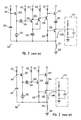
- FIG. 2 is a schematic diagram of a typical prior art medium speed output buffer.
- An input signal is applied to node N21 in order to control output pull up transistor 233 and output pull down transistor 235 which in turn source and sink, respectively, current to load 212.
- transistor 222 With a logical one input signal applied to node N21, transistor 222 turns on, causing diode 224 to reverse bias, causing pull up transistor 225 to supply base drive to transistor 226.
- Transistor 226 thus turns on, thereby turning off transistor 229, and in turn turning on phase splitter transistor 232.
- phase splitter transistor 232 With phase splitter transistor 232 turned on, pull up transistor 233 is turned off and pull down transistor is turned on, sinking current I load from load 212 through inductor 201 to ground 202.
- medium speed circuit 200 includes node N21 having a relatively large time constant, since capacitor 220 and pull up resistor 221 are relatively large. Circuit 200 also includes node N22 at the base of phase splitter transistor 232, which has a relatively small time constant, due to the rather small parasitic capacitance on node N22.
- FIG 3 is a circuit diagram of a typical prior art high speed output buffer.
- High speed output buffer 300 is similar to the medium speed output buffer 200 of Figure 2 except that the inversions provided by transistors 226 and 229 of Figure 2 are eliminated. This results in node N32 having a relatively large effective time constant, since node N32 follows node N31 through transistor 332 and diode 324. This has the effect of slowing the high to low transition of the output signal applied to load 312, while providing a low propagation delay.
- inductor 301 acts as a feedback impedance to the common emitter amplifier formed by transistors 332 and 335. Since node N32 has a large RC time constant, the voltage on node N32 acts as a small signal to the common emitter amplifier. The effect of the feedback impedance provided by inductor 301 reduces circuit gain and thus the output edge rate.
- Figure 5 is a diagram depicting the waveforms associates with high speed output buffer circuit 300 of Figure 3, showing a smaller propagation delay than that of Figure 4, but with an increased percentage of the total delay due to inductance effects.
- Figure 6 depicts a prior art integrated circuit lead frame 60 including two separate ground leads 61 and 62 for separate connections of grounds on an integrated circuit placed within cavity 64 of lead frame 60, for ultimate connection at pin 63 to a circuit ground.
- Such package has been used in the past in order to minimize ground noise problems.
- Figure 7 is a schematic diagram depicting a model of a typical prior art output circuit.
- a novel output buffer circuit which advantageously uses a simple integrated circuit package including two separate ground leads for connection to an externally supplied ground voltage.
- the relatively large pull down current which passes through the pull down transistor of one of more output buffers is fed through a first ground lead of the lead frame to the external ground and the remaining circuitry is connected to the external ground through the second ground lead of the lead frame. In this manner, the transients in the pull down current will cause ground bounce which affects the pull down transistor only, and not the remaining components of the output buffer.
- the amount of ground bounce is controlled to provide a desired characteristic of the output transition.
- FIG. 8 is a schematic diagram of one embodiment of an output buffer constructed in accordance with the teachings of this invention.
- Output buffer 800 includes ground inductance 803-1, corresponding to lead 61 of the integrated circuit package shown in Figure 6, for connecting external ground 802 to the driver circuitry of output buffer 800.
- Output buffer 800 also includes a second inductor 803-2 corresponding to lead 62 of the integrated circuit package shown in Figure 6 for connecting output pull down transistor 835 to external ground 802.
- Reference supply 882 provides a bias voltage V ref to the base of transistor 880 which is connected in a common emitter configuration with transistor 822 to current source 823. With a high signal applied to input node N81, transistor 822 turns on, causing transistor 880 to turn off, raising node N82 high.
- phase splitter transistor 832 This causes phase splitter transistor 832 to turn on, turning off output pull up transistor 833, and turning on output pulldown transistor 835.
- This causes pull down current I load to be sunk from load 812 through pull down transistor 835, through inductor 803-2, to ground 802.
- the ground bounce caused by inductor 803-2 is applied only to the emitter of output pull down transistor 835, and does not affect the components which are connected to ground through inductor 803-1 since there is no significant transient current through inductor 803-1 at this time.
- a small time constant and therefore a fast input edge rate is provided at node N82 due to its low capacitance, thereby allowing the high to low transition of the output voltage to be very rapid, thereby enhancing switching speed. Furthermore, this small time constant is provided at node N82 without the need for additional inversions between nodes N81 and N82, as is the case with the prior art medium speed output buffer circuit of Figure 2. Thus, without additional inversions between nodes N81 and N82, the propagation delay is reduced as compared with medium speed circuit 200 Figure 2.
- Figure 7 shows a portion of an output pull down transistor circuit 700 when pull down current I load is being conducted through pull down transistor 704 through package inductance 706 to ground 706.
- L dI/dt is small, limiting the range of charge removal from the output load, and therefore limiting the output edge rate.
- voltage V1 limits di/dt and therefore the speed of the high to low transition of the output voltage applied to load 707.
- V out is the output voltage applied to load 707, in order to provide maximum output switching speed.
- ground bounce should be maximized and the input edge rate should be maximized.
- the amount of ground bounce that a user of such a circuit can tolerate.
- ground bounce is desirably increased, in contrast to the thinking of the prior art. In order to achieve a distinct advantage, i.e., a very rapid high to low transition of the output voltage applied to the load.
- means is provided to control the voltage excursion on nodes N82 or N83, or means to control the rate at which the voltage are nodes N82 or N83.
- Such means include, for example, clamping the desired node to quiet ground 899, for example through one or more diodes or transistors.
- output edge rate/ground bounce is controlled by adding a capacitance in parallel with ground inductance 803-2, preferably in an amount equal to the sum of the load capacitances connected to the plurality of output buffers contained on an integrated circuit.
- a capacitance in parallel with ground inductance 803-2 preferably in an amount equal to the sum of the load capacitances connected to the plurality of output buffers contained on an integrated circuit.
- a smaller value of capacitance is connected to the base of transistors 832 or 835 and reflected through transistor 832 to inductor 803-2, thereby providing an effective capacitance equal to the value of the capacitance multiplied by the beta of transistor 835.
- FIG. 9 is a schematic diagram of another embodiment of an output pull down circuit constructed in accordance with the teachings of this invention.
- Output pull down circuit 900 of Figure 9 is similar to that of Figure 8, but includes transistor 990 and capacitor 991 in order to provide a transient current between the base of transistor 932 and inductor 903-2.
- Circuit elements 990 and 991 serve to prevent phase splitter transistor 932 from turning on during a brief period of time during which the emitter voltage of output pull down transistor 935 falls below ground 902. This occurs due to changes in ground current through other output circuits contained on the same integrated circuit. Such below-ground emitter voltage would ordinarily cause phase splitter transistor 932 to turn on even with relatively low voltage applied to its base.
- capacitor 991 supplies base drive to transistor 990 which turns on briefly in order to ensure that phase splitter transistor 932 remains turned off. Conversely, with the output voltage low, transistor 990 will not turn on even when noisy ground 998 changes voltage due to other output circuits switching current through package inductance 903-2.
- a means is provided to control the voltage excursion on node N92. By preventing the voltage on node N92 from exceeding a predetermined level, the edge rate of the output signal is controlled inversely to the amount of ground bounce permitted on the output signal.
- output edge rate/ground bounce is controlled by adding a capacitance in parallel with ground inductance 903-2, preferably in an amount equal to the sum of the load capacitances connected to the plurality of output buffers contained on an integrated circuit.
- a smaller value of capacitance is connected to the base of transistors 932 or 935 and beta multiplied.
- Figure 10 is a schematic diagram of an alternative embodiment of this invention, which is similar to that shown in Figure 9 and includes similar numbering.
- the embodiment of Figure 10 includes transistors 1001 and 1003, resistor 1002, and diode 1004 in order to prevent transistor 932 from inadvertently turning on when output terminal 917 is high. This may occur when noisy ground voltage present on node 998 glitches low with respect to quiet ground voltage present on node 999, for example when current I load in this or other output stages on the same integrated circuit begin to conduct an increased amount of current. During this time, the noisy ground voltage on node 998 goes lower with respect to the quiet ground voltage on node 999, thereby increasing the voltage across the base-emitter junction of transistor 932.
- transistor 1003 turns on due to its decreased emitter voltage, pulling down the base of transistor 932, preventing it from inadvertently turning on.
- Transistor 1001 and resistor 1002 provide base drive to transistor 1003, and diode 1004 clamps the base voltage of transistor 1003 to approximately 0.6 volts above the quiet ground voltage present on node 999.
Abstract
Description
- This invention relates to integrated circuits and more particularly to output buffer stages and the fall time of such output stages when the output voltage switches from a high to a low voltage.
- Figure 1 is a diagram depicting a typical
integrated circuit package 100 including an integrated circuit which has a plurality of output buffers 103-1 through 103-N. The ground lead of output buffers 103-1 through 103-N are connected to external ground 12 via a lead ofpackage 100 which has associated therewithinductance 101. Each output buffer 103-1 through 103-N is connected to an associated load 112-1 through 112-N, respectively. When current is sunk from one or more loads 112-1 through 112-N, that current flows toground 102 throughinductance 101. If all output buffers 103-1 through 103-N are sinking a load current Iload from loads 112-1 through 112-N,inductance 101 carriers a current N(Iload). - As is well known,
inductance 101 causes ground bounce, i.e., an increase in the effective ground voltage aboveground 102, when there is a change in the amount of current flowing throughinductor 101. If for example output buffer 103-1 is sinking current from load 112-1 in a steady state condition, load 112-1 is held to a voltage substantially equal to the voltage ofground 102. If then one or more of the other output buffers switches in order to sink additional current throughinductor 101, the "ground" voltage applied to load 112-1 will rise in voltage during the transient increase in current throughinductor 101. - Figure 2 is a schematic diagram of a typical prior art medium speed output buffer. An input signal is applied to node N21 in order to control output pull up
transistor 233 and output pull downtransistor 235 which in turn source and sink, respectively, current to load 212. With a logical one input signal applied to node N21,transistor 222 turns on, causingdiode 224 to reverse bias, causing pull up transistor 225 to supply base drive totransistor 226.Transistor 226 thus turns on, thereby turning offtransistor 229, and in turn turning onphase splitter transistor 232. Withphase splitter transistor 232 turned on, pull uptransistor 233 is turned off and pull down transistor is turned on, sinking current Iload fromload 212 through inductor 201 toground 202. This causes the voltage applied to load 212 to switch from a high to a low voltage, as shown in Figure 4. The delay between the time a high signal is applied to node N21 and the output voltage applied toload 212 goes low is caused by two mechanisms, the propagation delay through the circuitry between node N21 andoutput transistors - Of importance,
medium speed circuit 200 includes node N21 having a relatively large time constant, sincecapacitor 220 and pull upresistor 221 are relatively large.Circuit 200 also includes node N22 at the base ofphase splitter transistor 232, which has a relatively small time constant, due to the rather small parasitic capacitance on node N22. - Figure 3 is a circuit diagram of a typical prior art high speed output buffer. High
speed output buffer 300 is similar to the mediumspeed output buffer 200 of Figure 2 except that the inversions provided bytransistors transistor 332 anddiode 324. This has the effect of slowing the high to low transition of the output signal applied to load 312, while providing a low propagation delay. - Unfortunately, as current through
inductor 301 changes,inductor 301 acts as a feedback impedance to the common emitter amplifier formed bytransistors inductor 301 reduces circuit gain and thus the output edge rate. - Figure 5 is a diagram depicting the waveforms associates with high speed
output buffer circuit 300 of Figure 3, showing a smaller propagation delay than that of Figure 4, but with an increased percentage of the total delay due to inductance effects. - Figure 6 depicts a prior art integrated
circuit lead frame 60 including two separate ground leads 61 and 62 for separate connections of grounds on an integrated circuit placed withincavity 64 oflead frame 60, for ultimate connection atpin 63 to a circuit ground. Such package has been used in the past in order to minimize ground noise problems. - Figure 7 is a schematic diagram depicting a model of a typical prior art output circuit.
- In accordance with the teachings of this invention as defined in the independent claims, a novel output buffer circuit is taught which advantageously uses a simple integrated circuit package including two separate ground leads for connection to an externally supplied ground voltage. In accordance with the teachings of this invention, the relatively large pull down current which passes through the pull down transistor of one of more output buffers is fed through a first ground lead of the lead frame to the external ground and the remaining circuitry is connected to the external ground through the second ground lead of the lead frame. In this manner, the transients in the pull down current will cause ground bounce which affects the pull down transistor only, and not the remaining components of the output buffer. In this manner, base drive to the output pull down transistor is not decreased due to ground bounce, and the high to low transition of the output voltage is not degraded by the presence of ground bounce. In a specific embodiment, the amount of ground bounce is controlled to provide a desired characteristic of the output transition.
- Figure 1 is a diagram depicting a typical prior art output pull down structure;
- Figure 2 is a medium speed output buffer circuit at the prior art;
- Figure 3 is a high speed output circuit of the prior art;
- Figure 4 is a waveform depicting the switching of the circuit of Figure 3;
- Figure 5 is a wavefrom depicting the switching of the prior art circuit of Figure 3 and the improvement in switching speed contained in accordance with the teaching of this invention;
- Figure 6 depicts a prior art integrated circuit package including two separate ground leads connected to a single external ground pin;
- Figure 7 is a schematic diagram depicting a model of a typical prior art output circuit;
- Figure 8 is a schematic diagram depicting one embodiment of an output stage constructed in accordance with the teachings of this invention;
- Figure 9 is a schematic diagram of an alternative embodiment of an output circuit constructed in accordance with the teachings of this invention; and
- Figure 10 is a schematic diagram of an alternative embodiment of an output circuit constructed in accordance with the teachings of this invention.
- Figure 8 is a schematic diagram of one embodiment of an output buffer constructed in accordance with the teachings of this invention.
Output buffer 800 includes ground inductance 803-1, corresponding tolead 61 of the integrated circuit package shown in Figure 6, for connectingexternal ground 802 to the driver circuitry ofoutput buffer 800.Output buffer 800 also includes a second inductor 803-2 corresponding tolead 62 of the integrated circuit package shown in Figure 6 for connecting output pull downtransistor 835 toexternal ground 802.Reference supply 882 provides a bias voltage Vref to the base oftransistor 880 which is connected in a common emitter configuration withtransistor 822 tocurrent source 823. With a high signal applied to input node N81,transistor 822 turns on, causingtransistor 880 to turn off, raising node N82 high. This causesphase splitter transistor 832 to turn on, turning off output pull uptransistor 833, and turning onoutput pulldown transistor 835. This causes pull down current Iload to be sunk fromload 812 through pull downtransistor 835, through inductor 803-2, toground 802. The ground bounce caused by inductor 803-2 is applied only to the emitter of output pull downtransistor 835, and does not affect the components which are connected to ground through inductor 803-1 since there is no significant transient current through inductor 803-1 at this time. - In accordance with the teachings of this invention, a small time constant and therefore a fast input edge rate is provided at node N82 due to its low capacitance, thereby allowing the high to low transition of the output voltage to be very rapid, thereby enhancing switching speed. Furthermore, this small time constant is provided at node N82 without the need for additional inversions between nodes N81 and N82, as is the case with the prior art medium speed output buffer circuit of Figure 2. Thus, without additional inversions between nodes N81 and N82, the propagation delay is reduced as compared with
medium speed circuit 200 Figure 2. - The voltage relationships affecting the pull down output transistor are described now with reference to Figure 7. Figure 7 shows a portion of an output pull down
transistor circuit 700 when pull down current Iload is being conducted through pull downtransistor 704 throughpackage inductance 706 toground 706.
- Since V₂ cannot exceed V₁-Vbe when output pull down
transistor 704 is turned on, small values of V₁ (or slow rise times) limit the magnitude of V₂, and therefore the magnitude of the change in current throughpackage inductance 705, so

- For small V₁, L dI/dt is small, limiting the range of charge removal from the output load, and therefore limiting the output edge rate. Thus, for small swings of V₁ or slow low to high transitions of the input signal applied to
node 701, voltage V₁ limits di/dt and therefore the speed of the high to low transition of the output voltage applied toload 707. - It is desirable to maximize dVout/dt, where Vout is the output voltage applied to load 707, in order to provide maximum output switching speed. For a capacitive load

- Therefore, in order to achieve large output edge rates (high dVout/dt), the value of the noisy ground voltage V₂ must be high. from equation (6),
Combining equations (6) and (2)
thus
Therefore, in order to increase the output transition speed, the input transition speed (dV₁/dt) must be increased. - Therefore, in order to maximize the high to low transition speed of the output signal, ground bounce should be maximized and the input edge rate should be maximized. Naturally, there are limits to the amount of ground bounce that a user of such a circuit can tolerate. However, in accordance with the teachings of this invention, ground bounce is desirably increased, in contrast to the thinking of the prior art. In order to achieve a distinct advantage, i.e., a very rapid high to low transition of the output voltage applied to the load.
- In an alternative embodiment of this invention, means is provided to control the voltage excursion on nodes N82 or N83, or means to control the rate at which the voltage are nodes N82 or N83. Such means include, for example, clamping the desired node to
quiet ground 899, for example through one or more diodes or transistors. By preventing the voltage on node N82 from exceeding a predetermined level, the edge rate of the output signal is controlled inversely to the amount of ground bounce permitted on the output signal. - In another embodiment of this invention, output edge rate/ground bounce is controlled by adding a capacitance in parallel with ground inductance 803-2, preferably in an amount equal to the sum of the load capacitances connected to the plurality of output buffers contained on an integrated circuit. Naturally, such a technique is of most advantage when it is known what load capacitance is to be connected to each of the output terminals of the integrated circuit. However, even when this is not the case, for example when an integrated circuit is a relatively generic device that can be used in a number of systems having various load capacitances, an improvement can still be made by including a capacitance in parallel with ground inductance 803-2. In an alternative embodiment of this invention, a smaller value of capacitance is connected to the base of
transistors transistor 832 to inductor 803-2, thereby providing an effective capacitance equal to the value of the capacitance multiplied by the beta oftransistor 835. - Figure 9 is a schematic diagram of another embodiment of an output pull down circuit constructed in accordance with the teachings of this invention. Output pull down
circuit 900 of Figure 9 is similar to that of Figure 8, but includestransistor 990 andcapacitor 991 in order to provide a transient current between the base oftransistor 932 and inductor 903-2.Circuit elements phase splitter transistor 932 from turning on during a brief period of time during which the emitter voltage of output pull downtransistor 935 falls belowground 902. This occurs due to changes in ground current through other output circuits contained on the same integrated circuit. Such below-ground emitter voltage would ordinarily causephase splitter transistor 932 to turn on even with relatively low voltage applied to its base. With the inclusion ofcircuit elements time period capacitor 991 supplies base drive totransistor 990 which turns on briefly in order to ensure thatphase splitter transistor 932 remains turned off. Conversely, with the output voltage low,transistor 990 will not turn on even whennoisy ground 998 changes voltage due to other output circuits switching current through package inductance 903-2. - While the embodiments of this invention depicted in Figures 8 and 9 include both output pull up and pull down transistors, it is readily understood by those of ordinary skill in the art in light of the teachings of this invention that this invention applies equally well to open collector output stages as well.
- In an alternative embodiment of this invention, a means is provided to control the voltage excursion on node N92. By preventing the voltage on node N92 from exceeding a predetermined level, the edge rate of the output signal is controlled inversely to the amount of ground bounce permitted on the output signal.
- In another embodiment of this invention, output edge rate/ground bounce is controlled by adding a capacitance in parallel with ground inductance 903-2, preferably in an amount equal to the sum of the load capacitances connected to the plurality of output buffers contained on an integrated circuit. In an alternative embodiment of this invention, a smaller value of capacitance is connected to the base of
transistors - Figure 10 is a schematic diagram of an alternative embodiment of this invention, which is similar to that shown in Figure 9 and includes similar numbering. The embodiment of Figure 10, however, includes
transistors resistor 1002, anddiode 1004 in order to preventtransistor 932 from inadvertently turning on whenoutput terminal 917 is high. This may occur when noisy ground voltage present onnode 998 glitches low with respect to quiet ground voltage present onnode 999, for example when current Iload in this or other output stages on the same integrated circuit begin to conduct an increased amount of current. During this time, the noisy ground voltage onnode 998 goes lower with respect to the quiet ground voltage onnode 999, thereby increasing the voltage across the base-emitter junction oftransistor 932. At this time, in accordance with the teachings of the embodiment of Figure 10,transistor 1003 turns on due to its decreased emitter voltage, pulling down the base oftransistor 932, preventing it from inadvertently turning on.Transistor 1001 andresistor 1002 provide base drive totransistor 1003, anddiode 1004 clamps the base voltage oftransistor 1003 to approximately 0.6 volts above the quiet ground voltage present onnode 999. - Although the foregoing invention has been described in some detail by way of illustration and example for purposes of clarity of understanding, it will be readily apparent to those of ordinary skill in the art in light of the teachings of this invention that certain changes and modifications may be made thereto without departing from the spirit or scope of the appended claims.
Claims (17)
- An output circuit comprising:
a first supply voltage lead for receiving an externally supplied first supply voltage;
a second supply voltage lead for receiving an externally supplied second supply voltage;
a third supply voltage lead for receiving said externally supplied second supply voltage;
an input terminal for receiving an input signal;
an output terminal for providing an output signal in response to said input signal;
an output pull down transistor having a first current lead coupled to said output terminal, a second current lead for coupling to said externally supplied second supply voltage via said second supply voltage lead, and a control lead; and
means for providing a control signal to said control lead of said output pull down transistor in response to said input signal, said means for providing being coupled to said first supply voltage and also being coupled to said externally supplied second supply voltage via said third supply voltage lead. - A circuit as a in claim 1 which further comprises a first inductance coupled between said second supply voltage lead and said externally supplied second supply voltage, and a second inductance coupled between said third supply voltage lead and said externally supplied second supply voltage.
- A circuit as in claim 2 wherein said first and second inductances are provided by a first and a second package lead of a leadframe for housing a semiconductor device.
- A circuit as in claim 1 wherein said means for providing a control signal comprises a control transistor having a first current terminal coupled to said first supply voltage, a second current terminal coupled to said control lead of said output pull down transistor, and a control lead coupled to said input lead.
- A circuit as in claim 4 which further comprises means for limiting the voltage on said control lead of said control transistor.
- A circuit as in claim 1 which further comprises an output pull up transistor having a first current lead coupled to said output terminal, a second current lead coupled to said externally supplied first supply voltage via said first supply voltage lead, and a control lead, wherein said means for providing a control signal also provides a control signal to said control lead of said output pull up transistor in response to said input signal.
- A circuit as in claim 6 which further comprises a first inductance coupled between said second supply voltage lead and said externally supplied second supply voltage, and a second inductance coupled between said third supply voltage lead and said externally supplied second supply voltage.
- A circuit as in claim 7 wherein said first and second inductances are provided by a first and a second package lead of a leadframe for housing a semiconductor device.
- A circuit as in claim 6 wherein said means for providing a control signal comprises a control transistor having a first current terminal coupled to said first supply voltage, a second current terminal coupled to said control lead of said output pull down transistor, and a control lead coupled to said input lead.
- A circuit as in claim 9 which further comprises means for limiting the voltage on said control lead of said control transistor.
- A circuit as in claim 2 which further comprises a capacitance coupled in parallel with said first inductance.
- A circuit as in claim 11 wherein said capacitance is approximately equal to a load capacitance applied to said output terminal.
- A circuit as in claim 11 wherein said capacitance comprises a beta multipled capacitance.
- A method for controlling the output signal transition of an output circuit including an output pull down transistor, comprising the steps of:
providing a first ground voltage for selectively coupling to said output terminal via said output pull down transistor; and
providing a second ground voltage for coupling to circuitry driving said output pull down transistor, said second ground voltage being substantially constant regardless of changes in said first ground voltage. - A method as in claim 14 wherein said steps of providing comprise the steps of:
coupling an external ground voltage through a first inductance to provide said first ground voltage; and
coupling said external ground voltage through a second inductance to provide said second ground voltage. - A method as in claim 15 wherein said first and second inductances are provided by a leadframe for housing a semiconductor device.
- A method for increasing the transition speed of an output signal provided by an output pull down transistor comprising the step of increasing the ground bounce of a ground voltage applied to said pull down transistor.
Applications Claiming Priority (2)
| Application Number | Priority Date | Filing Date | Title |
|---|---|---|---|
| US07/512,786 US5089721A (en) | 1990-04-20 | 1990-04-20 | Ground bounce isolation and high speed output circuit |
| US512786 | 1990-04-20 |
Publications (2)
| Publication Number | Publication Date |
|---|---|
| EP0452747A2 true EP0452747A2 (en) | 1991-10-23 |
| EP0452747A3 EP0452747A3 (en) | 1991-12-04 |
Family
ID=24040559
Family Applications (1)
| Application Number | Title | Priority Date | Filing Date |
|---|---|---|---|
| EP19910105408 Withdrawn EP0452747A3 (en) | 1990-04-20 | 1991-04-05 | Ground bounce isolation network |
Country Status (4)
| Country | Link |
|---|---|
| US (1) | US5089721A (en) |
| EP (1) | EP0452747A3 (en) |
| JP (1) | JPH04229717A (en) |
| KR (1) | KR0182286B1 (en) |
Cited By (1)
| Publication number | Priority date | Publication date | Assignee | Title |
|---|---|---|---|---|
| CN108270423A (en) * | 2018-01-26 | 2018-07-10 | 广东美的制冷设备有限公司 | The Drive Protecting Circuit and air conditioner of IGBT module |
Families Citing this family (8)
| Publication number | Priority date | Publication date | Assignee | Title |
|---|---|---|---|---|
| US5168176A (en) * | 1991-07-23 | 1992-12-01 | Standard Microsystems Corporation | Apparatus and method to prevent the unsettling of a quiescent, low output channel caused by ground bounce induced by neighboring output channels |
| US5321320A (en) * | 1992-08-03 | 1994-06-14 | Unisys Corporation | ECL driver with adjustable rise and fall times, and method therefor |
| US5506521A (en) * | 1992-08-03 | 1996-04-09 | Unisys Corporation | ECL driver with adjustable rise and fall times, and method therefor |
| US5428303A (en) * | 1994-05-20 | 1995-06-27 | National Semiconductor Corporation | Bias generator for low ground bounce output driver |
| US6127876A (en) * | 1996-10-16 | 2000-10-03 | Texas Instruments Incorporated | Positive ground bounce compensation circuit for bipolar integrated devices |
| US6084439A (en) * | 1997-07-02 | 2000-07-04 | Cypress Semiconductor Corp. | Peak detector circuit with extended input voltage range |
| US6054874A (en) * | 1997-07-02 | 2000-04-25 | Cypress Semiconductor Corp. | Output driver circuit with switched current source |
| KR20230086406A (en) | 2021-12-08 | 2023-06-15 | 조하원 | Reduction composition for permanent and preparation method thereof |
Citations (7)
| Publication number | Priority date | Publication date | Assignee | Title |
|---|---|---|---|---|
| JPS60119692A (en) * | 1983-12-02 | 1985-06-27 | Hitachi Ltd | Semiconductor integrated circuit device |
| JPS61290820A (en) * | 1985-06-19 | 1986-12-20 | Hitachi Micro Comput Eng Ltd | Logic circuit |
| EP0214307A1 (en) * | 1985-02-28 | 1987-03-18 | Sony Corporation | Semiconducteur circuit device |
| EP0251880A2 (en) * | 1986-06-30 | 1988-01-07 | Fairchild Semiconductor Corporation | Reduction in power rail perturbation and in the effect thereof on integrated circuit performance |
| EP0284357A2 (en) * | 1987-03-23 | 1988-09-28 | Kabushiki Kaisha Toshiba | Semiconductor integrated circuit having a data output buffer circuit |
| JPH01161920A (en) * | 1987-12-18 | 1989-06-26 | Fujitsu Ltd | Ttl circuit |
| JPH02123823A (en) * | 1988-11-01 | 1990-05-11 | Nec Corp | Output circuit |
Family Cites Families (7)
| Publication number | Priority date | Publication date | Assignee | Title |
|---|---|---|---|---|
| US4613771A (en) * | 1984-04-18 | 1986-09-23 | Burroughs Corporation | Integrated circuit having three power bases and proportioned parasitic resistive and capacitive coupling to reduce output noise |
| US4609834A (en) * | 1984-12-24 | 1986-09-02 | Burroughs Corporation | Integrated logic circuit incorporating a module which generates a control signal that cancels switching noise |
| US4975603A (en) * | 1986-07-02 | 1990-12-04 | Texas Instruments Incorporated | Method and circuitry for compensating for negative internal ground voltage glitches |
| JPH01113993A (en) * | 1987-10-28 | 1989-05-02 | Toshiba Corp | Semiconductor integrated circuit |
| DE3739872A1 (en) * | 1987-11-25 | 1989-06-08 | Texas Instruments Deutschland | INTEGRATED CIRCUIT |
| US4862018A (en) * | 1987-11-30 | 1989-08-29 | Texas Instruments Incorporated | Noise reduction for output drivers |
| JP2511399Y2 (en) * | 1988-02-29 | 1996-09-25 | シャープ株式会社 | Comparator circuit |
-
1990
- 1990-04-20 US US07/512,786 patent/US5089721A/en not_active Expired - Lifetime
-
1991
- 1991-04-05 EP EP19910105408 patent/EP0452747A3/en not_active Withdrawn
- 1991-04-19 JP JP3179066A patent/JPH04229717A/en active Pending
- 1991-04-19 KR KR1019910006271A patent/KR0182286B1/en not_active IP Right Cessation
Patent Citations (7)
| Publication number | Priority date | Publication date | Assignee | Title |
|---|---|---|---|---|
| JPS60119692A (en) * | 1983-12-02 | 1985-06-27 | Hitachi Ltd | Semiconductor integrated circuit device |
| EP0214307A1 (en) * | 1985-02-28 | 1987-03-18 | Sony Corporation | Semiconducteur circuit device |
| JPS61290820A (en) * | 1985-06-19 | 1986-12-20 | Hitachi Micro Comput Eng Ltd | Logic circuit |
| EP0251880A2 (en) * | 1986-06-30 | 1988-01-07 | Fairchild Semiconductor Corporation | Reduction in power rail perturbation and in the effect thereof on integrated circuit performance |
| EP0284357A2 (en) * | 1987-03-23 | 1988-09-28 | Kabushiki Kaisha Toshiba | Semiconductor integrated circuit having a data output buffer circuit |
| JPH01161920A (en) * | 1987-12-18 | 1989-06-26 | Fujitsu Ltd | Ttl circuit |
| JPH02123823A (en) * | 1988-11-01 | 1990-05-11 | Nec Corp | Output circuit |
Non-Patent Citations (4)
| Title |
|---|
| PATENT ABSTRACTS OF JAPAN, vol. 11, no. 154 (E-508)[2601] 19 May 1987; & JP-A-61 290 820 (HITACHI MICRO COMPUT ENG LTD) 20.12.1986 * |
| PATENT ABSTRACTS OF JAPAN, vol. 13, no. 433 (E-824)[3781] 27 September 1989; & JP-A-01 161 920 (FUJITSU LTD) 26.06.1989 * |
| PATENT ABSTRACTS OF JAPAN, vol. 14, no. 354 (E-958)[4297] 31 July 1990; & JP-A-02 123 823 (NEC CORP.) 11.05.1990 * |
| PATENT ABSTRACTS OF JAPAN, vol. 9, no. 276 (P-402)[1999] 02 November 1985; & JP-A-60 119 692 (HITACHI SEISAKUSHO K.K.) 27.06.1985 * |
Cited By (1)
| Publication number | Priority date | Publication date | Assignee | Title |
|---|---|---|---|---|
| CN108270423A (en) * | 2018-01-26 | 2018-07-10 | 广东美的制冷设备有限公司 | The Drive Protecting Circuit and air conditioner of IGBT module |
Also Published As
| Publication number | Publication date |
|---|---|
| KR0182286B1 (en) | 1999-04-15 |
| US5089721A (en) | 1992-02-18 |
| KR910019344A (en) | 1991-11-30 |
| EP0452747A3 (en) | 1991-12-04 |
| JPH04229717A (en) | 1992-08-19 |
Similar Documents
| Publication | Publication Date | Title |
|---|---|---|
| US5321319A (en) | High speed CMOS bus driver circuit that provides minimum output signal oscillation | |
| US4791326A (en) | Current controlled solid state switch | |
| US4567378A (en) | Driver circuit for controlling signal rise and fall in field effect transistor processors | |
| US5319260A (en) | Apparatus and method to prevent the disturbance of a quiescent output buffer caused by ground bounce or by power bounce induced by neighboring active output buffers | |
| US5355029A (en) | Staged CMOS output buffer | |
| US5296765A (en) | Driver circuit for sinking current to two supply voltages | |
| JPH04345317A (en) | Driver circuit, low noise driver circuit and low noise low vibration driver-receiver circuit | |
| KR20010049227A (en) | Level adjustment circuit and data output circuit thereof | |
| JP2567153B2 (en) | CMOS output buffer circuit | |
| US5168176A (en) | Apparatus and method to prevent the unsettling of a quiescent, low output channel caused by ground bounce induced by neighboring output channels | |
| US5089721A (en) | Ground bounce isolation and high speed output circuit | |
| US5089724A (en) | High-speed low-power ECL/NTL circuits with AC-coupled complementary push-pull output stage | |
| JP2941579B2 (en) | Square law clamp circuit | |
| US5010256A (en) | Gate output driver using slew-rate control | |
| US6111453A (en) | Power switching device | |
| US5148048A (en) | CMOS output circuit having controlled slope | |
| EP0621693A2 (en) | BiCMOS output driver circuit | |
| US5517130A (en) | Method and structure for reducing noise in output buffer circuits | |
| US4877975A (en) | Logic circuit having an output signal with a gentle leading edge | |
| US5521539A (en) | Delay line providing an adjustable delay | |
| US5120998A (en) | Source terminated transmission line driver | |
| JPH03117915A (en) | Output stage control circuit | |
| US4975600A (en) | Bicmos TTL output driver circuit | |
| JPH03147422A (en) | Ecl circuit | |
| KR100265834B1 (en) | Input/output buffer in semiconductoe device |
Legal Events
| Date | Code | Title | Description |
|---|---|---|---|
| PUAI | Public reference made under article 153(3) epc to a published international application that has entered the european phase |
Free format text: ORIGINAL CODE: 0009012 |
|
| PUAL | Search report despatched |
Free format text: ORIGINAL CODE: 0009013 |
|
| AK | Designated contracting states |
Kind code of ref document: A2 Designated state(s): DE FR GB IT |
|
| AK | Designated contracting states |
Kind code of ref document: A3 Designated state(s): DE FR GB IT |
|
| 17P | Request for examination filed |
Effective date: 19920408 |
|
| 17Q | First examination report despatched |
Effective date: 19940715 |
|
| STAA | Information on the status of an ep patent application or granted ep patent |
Free format text: STATUS: THE APPLICATION IS DEEMED TO BE WITHDRAWN |
|
| 18D | Application deemed to be withdrawn |
Effective date: 19950126 |