EP0452043B1 - X-ray mask structure - Google Patents
X-ray mask structure Download PDFInfo
- Publication number
- EP0452043B1 EP0452043B1 EP91302999A EP91302999A EP0452043B1 EP 0452043 B1 EP0452043 B1 EP 0452043B1 EP 91302999 A EP91302999 A EP 91302999A EP 91302999 A EP91302999 A EP 91302999A EP 0452043 B1 EP0452043 B1 EP 0452043B1
- Authority
- EP
- European Patent Office
- Prior art keywords
- supporting frame
- ring
- mask substrate
- stress
- mask
- Prior art date
- Legal status (The legal status is an assumption and is not a legal conclusion. Google has not performed a legal analysis and makes no representation as to the accuracy of the status listed.)
- Expired - Lifetime
Links
- 239000000853 adhesive Substances 0.000 claims description 39
- 239000000758 substrate Substances 0.000 claims description 28
- 230000001070 adhesive effect Effects 0.000 claims description 17
- 239000000463 material Substances 0.000 claims description 13
- 230000008602 contraction Effects 0.000 claims description 7
- 230000035882 stress Effects 0.000 description 14
- 230000008646 thermal stress Effects 0.000 description 3
- 229910010272 inorganic material Inorganic materials 0.000 description 2
- 239000011147 inorganic material Substances 0.000 description 2
- 239000010409 thin film Substances 0.000 description 2
- 238000004026 adhesive bonding Methods 0.000 description 1
- 238000007599 discharging Methods 0.000 description 1
- 230000000694 effects Effects 0.000 description 1
- 238000005530 etching Methods 0.000 description 1
- 239000000395 magnesium oxide Substances 0.000 description 1
- 238000004519 manufacturing process Methods 0.000 description 1
- 238000000034 method Methods 0.000 description 1
- 238000012986 modification Methods 0.000 description 1
- 230000004048 modification Effects 0.000 description 1
- 230000002093 peripheral effect Effects 0.000 description 1
- 239000004065 semiconductor Substances 0.000 description 1
Images

Classifications
-
- G—PHYSICS
- G03—PHOTOGRAPHY; CINEMATOGRAPHY; ANALOGOUS TECHNIQUES USING WAVES OTHER THAN OPTICAL WAVES; ELECTROGRAPHY; HOLOGRAPHY
- G03F—PHOTOMECHANICAL PRODUCTION OF TEXTURED OR PATTERNED SURFACES, e.g. FOR PRINTING, FOR PROCESSING OF SEMICONDUCTOR DEVICES; MATERIALS THEREFOR; ORIGINALS THEREFOR; APPARATUS SPECIALLY ADAPTED THEREFOR
- G03F1/00—Originals for photomechanical production of textured or patterned surfaces, e.g., masks, photo-masks, reticles; Mask blanks or pellicles therefor; Containers specially adapted therefor; Preparation thereof
- G03F1/22—Masks or mask blanks for imaging by radiation of 100nm or shorter wavelength, e.g. X-ray masks, extreme ultraviolet [EUV] masks; Preparation thereof
-
- G—PHYSICS
- G03—PHOTOGRAPHY; CINEMATOGRAPHY; ANALOGOUS TECHNIQUES USING WAVES OTHER THAN OPTICAL WAVES; ELECTROGRAPHY; HOLOGRAPHY
- G03F—PHOTOMECHANICAL PRODUCTION OF TEXTURED OR PATTERNED SURFACES, e.g. FOR PRINTING, FOR PROCESSING OF SEMICONDUCTOR DEVICES; MATERIALS THEREFOR; ORIGINALS THEREFOR; APPARATUS SPECIALLY ADAPTED THEREFOR
- G03F7/00—Photomechanical, e.g. photolithographic, production of textured or patterned surfaces, e.g. printing surfaces; Materials therefor, e.g. comprising photoresists; Apparatus specially adapted therefor
- G03F7/70—Microphotolithographic exposure; Apparatus therefor
- G03F7/708—Construction of apparatus, e.g. environment aspects, hygiene aspects or materials
- G03F7/70858—Environment aspects, e.g. pressure of beam-path gas, temperature
- G03F7/70866—Environment aspects, e.g. pressure of beam-path gas, temperature of mask or workpiece
-
- Y—GENERAL TAGGING OF NEW TECHNOLOGICAL DEVELOPMENTS; GENERAL TAGGING OF CROSS-SECTIONAL TECHNOLOGIES SPANNING OVER SEVERAL SECTIONS OF THE IPC; TECHNICAL SUBJECTS COVERED BY FORMER USPC CROSS-REFERENCE ART COLLECTIONS [XRACs] AND DIGESTS
- Y10—TECHNICAL SUBJECTS COVERED BY FORMER USPC
- Y10T—TECHNICAL SUBJECTS COVERED BY FORMER US CLASSIFICATION
- Y10T428/00—Stock material or miscellaneous articles
- Y10T428/21—Circular sheet or circular blank
-
- Y—GENERAL TAGGING OF NEW TECHNOLOGICAL DEVELOPMENTS; GENERAL TAGGING OF CROSS-SECTIONAL TECHNOLOGIES SPANNING OVER SEVERAL SECTIONS OF THE IPC; TECHNICAL SUBJECTS COVERED BY FORMER USPC CROSS-REFERENCE ART COLLECTIONS [XRACs] AND DIGESTS
- Y10—TECHNICAL SUBJECTS COVERED BY FORMER USPC
- Y10T—TECHNICAL SUBJECTS COVERED BY FORMER US CLASSIFICATION
- Y10T428/00—Stock material or miscellaneous articles
- Y10T428/24—Structurally defined web or sheet [e.g., overall dimension, etc.]
- Y10T428/24479—Structurally defined web or sheet [e.g., overall dimension, etc.] including variation in thickness
- Y10T428/24612—Composite web or sheet
-
- Y—GENERAL TAGGING OF NEW TECHNOLOGICAL DEVELOPMENTS; GENERAL TAGGING OF CROSS-SECTIONAL TECHNOLOGIES SPANNING OVER SEVERAL SECTIONS OF THE IPC; TECHNICAL SUBJECTS COVERED BY FORMER USPC CROSS-REFERENCE ART COLLECTIONS [XRACs] AND DIGESTS
- Y10—TECHNICAL SUBJECTS COVERED BY FORMER USPC
- Y10T—TECHNICAL SUBJECTS COVERED BY FORMER US CLASSIFICATION
- Y10T428/00—Stock material or miscellaneous articles
- Y10T428/24—Structurally defined web or sheet [e.g., overall dimension, etc.]
- Y10T428/24802—Discontinuous or differential coating, impregnation or bond [e.g., artwork, printing, retouched photograph, etc.]
- Y10T428/24851—Intermediate layer is discontinuous or differential
Definitions
- This invention relates to an X-ray mask structure usable in an X-ray exposure apparatus for manufacture of semiconductor devices.
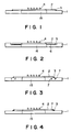
- Figure 1 shows an X-ray mask structure of known type.
- Denoted at 1 is a supporting frame
- denoted at 2 is a mask substrate
- denoted at 3 is an adhesive agent and denoted at 4 is a mask pattern.
- the mask substrate 2 is placed on the supporting frame 1, and the adhesive agent 3 is applied to the whole periphery of the mask substrate, whereby it is held fixed.
- the supporting frame 1 has a ring-like shape having an opening 15 formed at its center.
- the mask pattern 4 is formed of an X-ray absorptive material such as Au, for example, and it is formed on a thin film of a few micron thickness, made of an inorganic material such as SiN or SiC, for example.
- the mask substrate is formed of an inorganic material such as SiN or SiC, for example.
- the thin film can be formed by back-etching the mask substrate.
- the supporting frame 1 is provided by a Ti plate of a thickness of about 0.5 - 3 mm.
- Figure 2 shows another X-ray mask structure of known type.
- a recess 5 is formed in a supporting frame 1 and, in this recess 5, a mask substrate 2 is held fixed by using an adhesive agent layer 6.
- DE-A-3524196 is concerned with the problem of the reduction of the flatness of an X-ray mask when adhesive is allowed to flow over the mask and the support and describes arrangements in which an X-ray mask is secured by adhesive to a support formed with grooves provided at the adhesive bonding position to control the flow of adhesive so that the adhesive flows into the grooves rather than over the part of the surface carrying the mask pattern.
- an X-ray mask structure comprising a mask substrate having a pattern; a supporting frame for carrying and supporting said mask substrate; an adhesive material for fixing said mask substrate to said supporting frame; and stress releasing groove means provided in at least one of said mask substrate and said supporting frame; characterized in that said groove means delimit a plurality of adhesive material applying portions to which said adhesive material is applied and which are deformable to release stress due to differential thermal expansion between said mask substrate and said supporting frame and stress caused by contraction of said adhesive material whilst setting.
- Figure 1 is a sectional view of an X-ray mask structure of known type.
- Figure 2 is a sectional view of another X-ray mask structure of known type.
- Figure 3 is a sectional view of an X-ray mask structure according to a first embodiment of the present invention.
- Figure 4 is a sectional view of an X-ray mask structure according to a second embodiment of the present invention.
- Figure 5 is a top plan view of a supporting frame of the Figure 3 embodiment.
- Figure 6 is a top plan view of a supporting frame, in a modified form of the Figure 3 embodiment.
- Figure 7 is a sectional view of an X-ray mask structure according to a third embodiment of the present invention.
- Figure 8 is a sectional view of an X-ray mask structure according to a fourth embodiment of the present invention.
- Figure 3 shows a first embodiment of the present invention. Like numerals as those of Figure 1 are assigned to similar or corresponding elements, and explanation therefor is omitted here.
- Mask substrate 2 and supporting frame 1 are fixed to each other by means of an adhesive agent 3.
- a slit-like stress releasing groove 7 is formed in a portion of the supporting frame 1 adjacent the adhesive agent material 3.
- Such a stress releasing groove may be formed by using electric discharging technique, for example.
- Figure 5 is a top plan view of the supporting frame 1.
- Figure 3 corresponds to the section taken on a line A-A in Figure 5.
- the stress releasing groove 7 has a ring-like shape and, at eight points along the ring, adhesive agent applying portions 14 are defined.
- the surface of each adhesive agent applying portion 14 is divided from the surface of the surrounding portion of the supporting frame 1 by the provision of the stress releasing groove 7. Therefore, each adhesive agent applying portion 14 can be deformed relatively easily.
- Figure 6 is a top plan view showing another example of stress releasing groove 7.
- two ring-like grooves 7 are formed in continuous form, wherein at four sites the two ring-like grooves 7 are connected with each other by means of connection grooves 7a.
- an adhesive agent is applied to the peripheral portion of the mask substrate at adhesive agent applying portions 14 as illustrated.
- Figure 4 shows a second embodiment of the present invention.
- a stress releasing groove 7 is formed in a mask substrate 2.
- the remaining portion of this embodiment is essentially the same as the Figure 3 embodiment, in respect to structure and operation.
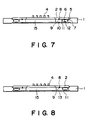
- Figure 7 shows a third embodiment of the present invention.
- a recess 5 is formed in a supporting frame 1 and, in this recess 5, a mask substrate 2 is fixed by using an adhesive agent layer 6.
- Stress releasing grooves 7 are formed in the supporting frame 1, at the opposite sides of the adhesive agent layer 6, as illustrated.
- the mask substrate 2 has alignment marks 8 formed thereon which are to be aligned with alignment marks 9, provided on the supporting frame 1, for the mutual positioning of the mask substrate 2 and the supporting frame 1.
- a viewangle controlling plate 11 is fixed by means of an adhesive agent layer 12.
- the viewangle controlling plate 11 also has alignment marks 10 formed thereon which are to be aligned with the marks 9 of the supporting frame 1, for the mutual positioning of the supporting frame 1 and the viewangle controlling plate 11.
- throughbores 13 may be formed in the plate as shown in Figure 8.
- a slit-like groove or grooves are formed adjacent to an adhesive agent material for adhering a mask substrate and a supporting frame to each other. Therefore, undesirable distortion or strain of the mask substrate and/or the supporting frame due to a thermal stress or a stress resulting from contraction of the adhesive agent when it is set, can be absorbed or released. It is therefore possible to attain high-precision and high-reliability pattern exposure transfer.
Description
- This invention relates to an X-ray mask structure usable in an X-ray exposure apparatus for manufacture of semiconductor devices.
- Figure 1 shows an X-ray mask structure of known type. Denoted at 1 is a supporting frame, denoted at 2 is a mask substrate, denoted at 3 is an adhesive agent and denoted at 4 is a mask pattern. The
mask substrate 2 is placed on the supporting frame 1, and theadhesive agent 3 is applied to the whole periphery of the mask substrate, whereby it is held fixed. The supporting frame 1 has a ring-like shape having an opening 15 formed at its center. Themask pattern 4 is formed of an X-ray absorptive material such as Au, for example, and it is formed on a thin film of a few micron thickness, made of an inorganic material such as SiN or SiC, for example. Also, the mask substrate is formed of an inorganic material such as SiN or SiC, for example. The thin film can be formed by back-etching the mask substrate. The supporting frame 1 is provided by a Ti plate of a thickness of about 0.5 - 3 mm. - Figure 2 shows another X-ray mask structure of known type. In this example, a
recess 5 is formed in a supporting frame 1 and, in thisrecess 5, amask substrate 2 is held fixed by using anadhesive agent layer 6. - In the X-ray mask structures as described above, there is a difference in coefficient of thermal expansion between the mask substrate and the supporting frame due to a difference in material. Thus, a temperature change causes a thermal stress in the X-ray mask structure, resulting in strain or distortion of the mask pattern. Further, possible contraction of the adhesive agent when the same is set causes a stress in the X-ray mask structure, also resulting in strain or distortion of the mask pattern.
- Particularly in a case where an adhesive agent is applied to the whole periphery of a mask substrate, such as in the example of Figure 1, non-uniformity in the thickness of the adhesive agent causes variation in quantity of contraction of the adhesive agent when it is set. Thus, by the contraction, an additional stress is applied which results in enlarged pattern distortion. In a case where an adhesive agent layer is provided as in the example of Figure 2, there is a disadvantage that, when the adhesive agent contracts, the flatness of the mask pattern bearing surface is degraded considerably.
- The English language abstract from Patents Abstracts of Japan
Volume 11 No. 244 (E-530) for Japanese Patent Application Publication No. 62-054919 describes an arrangement wherein an X-ray mask is secured to a support by adhesive which is received in adhesive retaining grooves of the support. The adhesive retaining grooves communicate with through holes of the support to allow release of excess adhesive. - DE-A-3524196 is concerned with the problem of the reduction of the flatness of an X-ray mask when adhesive is allowed to flow over the mask and the support and describes arrangements in which an X-ray mask is secured by adhesive to a support formed with grooves provided at the adhesive bonding position to control the flow of adhesive so that the adhesive flows into the grooves rather than over the part of the surface carrying the mask pattern.
- It is accordingly a primary object of the present invention to provide an improved X-ray mask structure by which the effect of a thermal stress or a stress due to contraction of an adhesive agent, can be reduced.
- According to the present invention, there is provided an X-ray mask structure, comprising a mask substrate having a pattern; a supporting frame for carrying and supporting said mask substrate; an adhesive material for fixing said mask substrate to said supporting frame; and stress releasing groove means provided in at least one of said mask substrate and said supporting frame; characterized in that said groove means delimit a plurality of adhesive material applying portions to which said adhesive material is applied and which are deformable to release stress due to differential thermal expansion between said mask substrate and said supporting frame and stress caused by contraction of said adhesive material whilst setting.
- Embodiments of the present invention will now be described with reference to the accompanying drawings in which:-
- Figure 1 is a sectional view of an X-ray mask structure of known type.
- Figure 2 is a sectional view of another X-ray mask structure of known type.
- Figure 3 is a sectional view of an X-ray mask structure according to a first embodiment of the present invention.
- Figure 4 is a sectional view of an X-ray mask structure according to a second embodiment of the present invention.
- Figure 5 is a top plan view of a supporting frame of the Figure 3 embodiment.
- Figure 6 is a top plan view of a supporting frame, in a modified form of the Figure 3 embodiment.
- Figure 7 is a sectional view of an X-ray mask structure according to a third embodiment of the present invention.
- Figure 8 is a sectional view of an X-ray mask structure according to a fourth embodiment of the present invention.
- Figure 3 shows a first embodiment of the present invention. Like numerals as those of Figure 1 are assigned to similar or corresponding elements, and explanation therefor is omitted here.
Mask substrate 2 and supporting frame 1 are fixed to each other by means of anadhesive agent 3. In a portion of the supporting frame 1 adjacent theadhesive agent material 3, a slit-likestress releasing groove 7 is formed. Such a stress releasing groove may be formed by using electric discharging technique, for example. Figure 5 is a top plan view of the supporting frame 1. Figure 3 corresponds to the section taken on a line A-A in Figure 5. As illustrated, thestress releasing groove 7 has a ring-like shape and, at eight points along the ring, adhesiveagent applying portions 14 are defined. As seen in Figure 5, the surface of each adhesiveagent applying portion 14 is divided from the surface of the surrounding portion of the supporting frame 1 by the provision of thestress releasing groove 7. Therefore, each adhesiveagent applying portion 14 can be deformed relatively easily. - Figure 6 is a top plan view showing another example of
stress releasing groove 7. In this example, two ring-like grooves 7 are formed in continuous form, wherein at four sites the two ring-like grooves 7 are connected with each other by means ofconnection grooves 7a. In this example, an adhesive agent is applied to the peripheral portion of the mask substrate at adhesiveagent applying portions 14 as illustrated. - Figure 4 shows a second embodiment of the present invention. In this embodiment, a
stress releasing groove 7 is formed in amask substrate 2. The remaining portion of this embodiment is essentially the same as the Figure 3 embodiment, in respect to structure and operation. - Figure 7 shows a third embodiment of the present invention. In this embodiment, a
recess 5 is formed in a supporting frame 1 and, in thisrecess 5, amask substrate 2 is fixed by using anadhesive agent layer 6.Stress releasing grooves 7 are formed in the supporting frame 1, at the opposite sides of theadhesive agent layer 6, as illustrated. Themask substrate 2 hasalignment marks 8 formed thereon which are to be aligned withalignment marks 9, provided on the supporting frame 1, for the mutual positioning of themask substrate 2 and the supporting frame 1. Also, to the bottom face of the supporting frame 1, aviewangle controlling plate 11 is fixed by means of anadhesive agent layer 12. Theviewangle controlling plate 11 also hasalignment marks 10 formed thereon which are to be aligned with themarks 9 of the supporting frame 1, for the mutual positioning of the supporting frame 1 and theviewangle controlling plate 11. In place of providing thealignment marks 10 of theviewangle controlling plate 11,throughbores 13 may be formed in the plate as shown in Figure 8. - In accordance with the present invention, as described hereinbefore, a slit-like groove or grooves are formed adjacent to an adhesive agent material for adhering a mask substrate and a supporting frame to each other. Therefore, undesirable distortion or strain of the mask substrate and/or the supporting frame due to a thermal stress or a stress resulting from contraction of the adhesive agent when it is set, can be absorbed or released. It is therefore possible to attain high-precision and high-reliability pattern exposure transfer.
- While the invention has been described with reference to the structures disclosed herein, it is not confined to the details set forth and this application is intended to cover such modifications or changes as come within the scope of the following claims.
Claims (5)
- An X-ray mask structure, comprising a mask substrate (2) having a pattern (4); a supporting frame (1) for carrying and supporting said mask substrate (2); an adhesive material (3) for fixing said mask substrate to said supporting frame; and stress releasing groove means (7) provided in at least one of said mask substrate (2) and said supporting frame (1); characterized in that said groove means (7) delimit a plurality of adhesive material applying portions (14) to which said adhesive material (3) is applied and which are deformable to release stress due to differential thermal expansion between said mask substrate (2) and said supporting frame (1) and stress caused by contraction of said adhesive material (3) whilst setting.
- An X-ray mask structure according to claim 1, wherein said supporting frame (1) has a ring-like shape and wherein said stress releasing groove means (7) is formed in a ring-like shape, concentric with the ring-like shape of said supporting frame (1).
- An X-ray mask structure according to claim 1, wherein said supporting frame (1) has a ring-like shape and the stress relieving groove means (7) comprises a ring-like groove concentric with the supporting frame (1), a number of subsidiary ring-like grooves communicating with the ring-like groove being disposed about the ring-like groove so as each to bound an adhesive material receiving portion (14) of the at least one of said mask substrate (2) and said supporting frame (1).
- An X-ray mask structure according to claim 1, wherein said stress relieving groove means (7) comprises two ring-like grooves connected to each other by means of connection grooves (7a).
- An X-ray mask structure according to any one of the preceding claims, wherein the supporting frame (1) is formed with a recess (5) for receiving the mask substrate (2).
Applications Claiming Priority (2)
| Application Number | Priority Date | Filing Date | Title |
|---|---|---|---|
| JP9201790A JP2911954B2 (en) | 1990-04-09 | 1990-04-09 | X-ray mask structure |
| JP92017/90 | 1990-04-09 |
Publications (2)
| Publication Number | Publication Date |
|---|---|
| EP0452043A1 EP0452043A1 (en) | 1991-10-16 |
| EP0452043B1 true EP0452043B1 (en) | 1997-07-23 |
Family
ID=14042765
Family Applications (1)
| Application Number | Title | Priority Date | Filing Date |
|---|---|---|---|
| EP91302999A Expired - Lifetime EP0452043B1 (en) | 1990-04-09 | 1991-04-05 | X-ray mask structure |
Country Status (4)
| Country | Link |
|---|---|
| US (1) | US5356686A (en) |
| EP (1) | EP0452043B1 (en) |
| JP (1) | JP2911954B2 (en) |
| DE (1) | DE69126907T2 (en) |
Families Citing this family (18)
| Publication number | Priority date | Publication date | Assignee | Title |
|---|---|---|---|---|
| JPH0567561A (en) * | 1991-09-10 | 1993-03-19 | Canon Inc | X-ray mask substrate, its manufacture and x-ray mask |
| EP0677787B1 (en) * | 1994-03-15 | 1998-10-21 | Canon Kabushiki Kaisha | Mask and mask supporting mechanism |
| JP3291408B2 (en) * | 1994-04-04 | 2002-06-10 | キヤノン株式会社 | Exposure apparatus and integrated circuit manufacturing method |
| JP2681619B2 (en) * | 1995-02-20 | 1997-11-26 | 東京エレクトロン株式会社 | Probe device |
| JP3261948B2 (en) * | 1995-03-28 | 2002-03-04 | キヤノン株式会社 | X-ray exposure mask and method for manufacturing semiconductor device using the same |
| US5854819A (en) * | 1996-02-07 | 1998-12-29 | Canon Kabushiki Kaisha | Mask supporting device and correction method therefor, and exposure apparatus and device producing method utilizing the same |
| US6317479B1 (en) | 1996-05-17 | 2001-11-13 | Canon Kabushiki Kaisha | X-ray mask, and exposure method and apparatus using the same |
| KR0170594B1 (en) * | 1996-05-25 | 1999-03-20 | 양승택 | Structure of glass ring for mask |
| US6101237A (en) * | 1996-08-28 | 2000-08-08 | Canon Kabushiki Kaisha | X-ray mask and X-ray exposure method using the same |
| JP3450648B2 (en) | 1997-05-09 | 2003-09-29 | キヤノン株式会社 | Magnification correction apparatus, X-ray exposure apparatus equipped with magnification correction apparatus, and device manufacturing method |
| JP3348783B2 (en) | 1999-07-28 | 2002-11-20 | 日本電気株式会社 | Mark for overlay and semiconductor device |
| JP2001100395A (en) | 1999-09-30 | 2001-04-13 | Toshiba Corp | Mask for exposure and method for manufacturing the same |
| JP2003007597A (en) * | 2001-06-25 | 2003-01-10 | Canon Inc | Method and device for multiplying mask pattern partially and mask structure |
| JP4463492B2 (en) * | 2003-04-10 | 2010-05-19 | 株式会社半導体エネルギー研究所 | Manufacturing equipment |
| JP4752491B2 (en) * | 2005-12-22 | 2011-08-17 | 株式会社ニコン | Device manufacturing method, mask, device |
| CN102436133A (en) * | 2011-08-17 | 2012-05-02 | 上海华力微电子有限公司 | Method for preventing movement of main graphics caused by stress transferred by photomask version |
| CN102436134A (en) * | 2011-08-29 | 2012-05-02 | 上海华力微电子有限公司 | Method for preventing photomask from being damaged by stress in non-light-transmitting cutting channel |
| JP6185498B2 (en) * | 2015-02-12 | 2017-08-23 | 株式会社半導体エネルギー研究所 | Evaporation mask |
Family Cites Families (4)
| Publication number | Priority date | Publication date | Assignee | Title |
|---|---|---|---|---|
| DE3524196C3 (en) * | 1984-07-06 | 1994-08-04 | Canon Kk | Lithography mask |
| US5012500A (en) * | 1987-12-29 | 1991-04-30 | Canon Kabushiki Kaisha | X-ray mask support member, X-ray mask, and X-ray exposure process using the X-ray mask |
| EP0323264B1 (en) * | 1987-12-29 | 1997-05-14 | Canon Kabushiki Kaisha | X-ray exposure process using an electrically conductive x-ray mask |
| EP0338749A3 (en) * | 1988-04-18 | 1990-05-02 | Canon Kabushiki Kaisha | Structure of x-ray mask |
-
1990
- 1990-04-09 JP JP9201790A patent/JP2911954B2/en not_active Expired - Fee Related
-
1991
- 1991-04-05 EP EP91302999A patent/EP0452043B1/en not_active Expired - Lifetime
- 1991-04-05 DE DE69126907T patent/DE69126907T2/en not_active Expired - Fee Related
-
1994
- 1994-01-14 US US08/182,513 patent/US5356686A/en not_active Expired - Fee Related
Also Published As
| Publication number | Publication date |
|---|---|
| EP0452043A1 (en) | 1991-10-16 |
| DE69126907T2 (en) | 1997-12-04 |
| JPH03290918A (en) | 1991-12-20 |
| US5356686A (en) | 1994-10-18 |
| DE69126907D1 (en) | 1997-08-28 |
| JP2911954B2 (en) | 1999-06-28 |
Similar Documents
| Publication | Publication Date | Title |
|---|---|---|
| EP0452043B1 (en) | X-ray mask structure | |
| US5374829A (en) | Vacuum chuck | |
| US6867848B2 (en) | Supporting structure of optical element, exposure apparatus having the same, and manufacturing method of semiconductor device | |
| JP5255565B2 (en) | Adjustable lens manufacturing method | |
| EP0769817B1 (en) | Method of manufacturing a photoelectric conversion apparatus | |
| US5721446A (en) | Semiconductor pressure sensor with spacing member disposed between sensor and substrate | |
| US4268563A (en) | Radiation mask for producing structural configurations in photo-sensitive resists by X-ray exposure | |
| US6030851A (en) | Method for overpressure protected pressure sensor | |
| KR20010062591A (en) | Stamp device for printing a pattern on a surface of a substrate | |
| US6303196B1 (en) | Pellicle | |
| JPH01292343A (en) | Pellicle | |
| KR0174299B1 (en) | Mask and mask supporting mechanism | |
| EP0453133B1 (en) | Method and apparatus for manufacture of X-ray mask | |
| JP2536434B2 (en) | Semiconductor substrate polishing equipment | |
| JPH0351287B2 (en) | ||
| US5305021A (en) | Thermal head | |
| KR19980015311A (en) | X-ray mask | |
| JPH0123137Y2 (en) | ||
| JP3431039B2 (en) | Optical encoder | |
| JPH08211214A (en) | Production of curved face grating | |
| WO1997014077A9 (en) | Magnification control and thermal substrate chuck for photolithography | |
| WO1997014077A1 (en) | Magnification control and thermal substrate chuck for photolithography | |
| JPH05619Y2 (en) | ||
| JPH02168614A (en) | Mask for x-ray exposure and exposing method using same | |
| KR100198812B1 (en) | X-ray mask |
Legal Events
| Date | Code | Title | Description |
|---|---|---|---|
| PUAI | Public reference made under article 153(3) epc to a published international application that has entered the european phase |
Free format text: ORIGINAL CODE: 0009012 |
|
| AK | Designated contracting states |
Kind code of ref document: A1 Designated state(s): DE FR GB IT NL |
|
| 17P | Request for examination filed |
Effective date: 19920309 |
|
| 17Q | First examination report despatched |
Effective date: 19940902 |
|
| GRAG | Despatch of communication of intention to grant |
Free format text: ORIGINAL CODE: EPIDOS AGRA |
|
| GRAH | Despatch of communication of intention to grant a patent |
Free format text: ORIGINAL CODE: EPIDOS IGRA |
|
| GRAH | Despatch of communication of intention to grant a patent |
Free format text: ORIGINAL CODE: EPIDOS IGRA |
|
| GRAA | (expected) grant |
Free format text: ORIGINAL CODE: 0009210 |
|
| AK | Designated contracting states |
Kind code of ref document: B1 Designated state(s): DE FR GB IT NL |
|
| PG25 | Lapsed in a contracting state [announced via postgrant information from national office to epo] |
Ref country code: IT Free format text: LAPSE BECAUSE OF FAILURE TO SUBMIT A TRANSLATION OF THE DESCRIPTION OR TO PAY THE FEE WITHIN THE PRESCRIBED TIME-LIMIT;WARNING: LAPSES OF ITALIAN PATENTS WITH EFFECTIVE DATE BEFORE 2007 MAY HAVE OCCURRED AT ANY TIME BEFORE 2007. THE CORRECT EFFECTIVE DATE MAY BE DIFFERENT FROM THE ONE RECORDED. Effective date: 19970723 Ref country code: FR Effective date: 19970723 |
|
| REF | Corresponds to: |
Ref document number: 69126907 Country of ref document: DE Date of ref document: 19970828 |
|
| EN | Fr: translation not filed | ||
| PLBE | No opposition filed within time limit |
Free format text: ORIGINAL CODE: 0009261 |
|
| STAA | Information on the status of an ep patent application or granted ep patent |
Free format text: STATUS: NO OPPOSITION FILED WITHIN TIME LIMIT |
|
| 26N | No opposition filed | ||
| REG | Reference to a national code |
Ref country code: GB Ref legal event code: IF02 |
|
| PGFP | Annual fee paid to national office [announced via postgrant information from national office to epo] |
Ref country code: GB Payment date: 20030324 Year of fee payment: 13 |
|
| PGFP | Annual fee paid to national office [announced via postgrant information from national office to epo] |
Ref country code: DE Payment date: 20030424 Year of fee payment: 13 |
|
| PGFP | Annual fee paid to national office [announced via postgrant information from national office to epo] |
Ref country code: NL Payment date: 20030430 Year of fee payment: 13 |
|
| PG25 | Lapsed in a contracting state [announced via postgrant information from national office to epo] |
Ref country code: GB Free format text: LAPSE BECAUSE OF NON-PAYMENT OF DUE FEES Effective date: 20040405 |
|
| PG25 | Lapsed in a contracting state [announced via postgrant information from national office to epo] |
Ref country code: NL Free format text: LAPSE BECAUSE OF NON-PAYMENT OF DUE FEES Effective date: 20041101 |
|
| PG25 | Lapsed in a contracting state [announced via postgrant information from national office to epo] |
Ref country code: DE Free format text: LAPSE BECAUSE OF NON-PAYMENT OF DUE FEES Effective date: 20041103 |
|
| GBPC | Gb: european patent ceased through non-payment of renewal fee | ||
| NLV4 | Nl: lapsed or anulled due to non-payment of the annual fee |
Effective date: 20041101 |