EP0450901A2 - Optical scanning system - Google Patents
Optical scanning system Download PDFInfo
- Publication number
- EP0450901A2 EP0450901A2 EP91302859A EP91302859A EP0450901A2 EP 0450901 A2 EP0450901 A2 EP 0450901A2 EP 91302859 A EP91302859 A EP 91302859A EP 91302859 A EP91302859 A EP 91302859A EP 0450901 A2 EP0450901 A2 EP 0450901A2
- Authority
- EP
- European Patent Office
- Prior art keywords
- optical
- deflecting member
- scanning system
- light deflecting
- motor
- Prior art date
- Legal status (The legal status is an assumption and is not a legal conclusion. Google has not performed a legal analysis and makes no representation as to the accuracy of the status listed.)
- Granted
Links
Images


Classifications
-
- G—PHYSICS
- G02—OPTICS
- G02B—OPTICAL ELEMENTS, SYSTEMS OR APPARATUS
- G02B7/00—Mountings, adjusting means, or light-tight connections, for optical elements
- G02B7/18—Mountings, adjusting means, or light-tight connections, for optical elements for prisms; for mirrors
- G02B7/182—Mountings, adjusting means, or light-tight connections, for optical elements for prisms; for mirrors for mirrors
- G02B7/1821—Mountings, adjusting means, or light-tight connections, for optical elements for prisms; for mirrors for mirrors for rotating or oscillating mirrors
-
- G—PHYSICS
- G02—OPTICS
- G02B—OPTICAL ELEMENTS, SYSTEMS OR APPARATUS
- G02B26/00—Optical devices or arrangements for the control of light using movable or deformable optical elements
- G02B26/08—Optical devices or arrangements for the control of light using movable or deformable optical elements for controlling the direction of light
- G02B26/10—Scanning systems
- G02B26/108—Scanning systems having one or more prisms as scanning elements
-
- G—PHYSICS
- G06—COMPUTING; CALCULATING OR COUNTING
- G06K—GRAPHICAL DATA READING; PRESENTATION OF DATA; RECORD CARRIERS; HANDLING RECORD CARRIERS
- G06K7/00—Methods or arrangements for sensing record carriers, e.g. for reading patterns
- G06K7/10—Methods or arrangements for sensing record carriers, e.g. for reading patterns by electromagnetic radiation, e.g. optical sensing; by corpuscular radiation
- G06K7/10544—Methods or arrangements for sensing record carriers, e.g. for reading patterns by electromagnetic radiation, e.g. optical sensing; by corpuscular radiation by scanning of the records by radiation in the optical part of the electromagnetic spectrum
- G06K7/10554—Moving beam scanning
- G06K7/10594—Beam path
- G06K7/10603—Basic scanning using moving elements
- G06K7/10633—Basic scanning using moving elements by oscillation
- G06K7/10643—Activating means
Definitions
- the present invention relates to an optical scanning system to be incorporated into an electrophotographic apparatus or a bar-code scanner.
- Electrophotography capable of printing in a high print quality has recently been developed. Electrophotography employs an optical scanning system to form an image.
- the optical scanning system has a light deflecting member mounted on the output shaft of a motor and disposed on the passage of a light beam emitted by a light source, such as a semiconductor laser.
- the light reflecting member reflects the light beam on an image plane, such as a photoconductive surface or a surface marked with a bar code.
- a polygonal rotating mirror when used as the light deflecting member is capable of reflecting light beams by its plurality of reflecting surfaces at a high frequency. However, it is difficult to correct the inevitable difference in characteristics between the plurality of reflecting surfaces.
- it is difficult to construct the optical scanning system employing a polygonal rotating mirror in a compact construction because optical parts including a semiconductor laser and a collimator lens must be arranged near the motor for rotating the polygonal rotating mirror.
- Figs. 10 and 11 show an optical scanning system incorporating improvements to solve those problems disclosed in Japanese Patent Laid-open No. 62-257119.
- this known optical scanning system 1 has a transparent member 2, i.e., a light deflecting member, attached to the output shaft of a motor, not shown.
- One end of the transparent member 2 is cut diagonally to form a reflecting surface 3 inclined at an angle of 45° to the axis of the transparent member 2.
- a portion of the circumference of the transparent member 2 extending at an acute angle, i.e., 45°, to the reflecting surface 3 is formed in a cylindroid surface 4.
- the center of rotation of the transparent member 2 is dislocated from the optical axis of a laser light source, not shown, for the layout of other parts and optical paths.
- a scanning light beam traveling along the axis of the transparent member 2 falls on the reflecting surface 3 of the rotating transparent member 2, and the scanning light beam is reflected by the reflecting surface 3 for scanning.
- the scanning light beam reflected by the reflecting surface 3 is refracted at the cylindroid surface 4.
- Optical scanning systems employing a polygonal rotating mirror as a light deflecting member are classified into those of a postobjective type and those of a preobjective type.
- An optical scanning system employing a light deflecting member having a reflecting surface wich receives a light beam along an optical path inclined to the center of rotation of the reflecting surface needs a correcting optical system because such an optical scanning system causes aberration, such as the curvature of image field.
- the optical scanning system 1 corrects the aberration of the scanning light beam reflected by the reflecting surface 3 by the refractive power of the cylindroid surface 4.
- Figs. 12 and 13 show another known optical scanning system disclosed in Japanese Patent Laid-open No. 1-283512.
- this known optical scanning system 5 employs a reflecting mirror 7, i.e., a light deflecting member, having a reflecting surface 6 inclined at an angle of 45° to its axis.
- the reflecting mirror 7 is attached to the output shaft of a motor 8.
- a tubular member 9 provided with a slit 10 in its circumference at a position corresponding to the reflecting surface 6 is attached to the upper surface of the motor 8 so as to enclose the reflecting mirror 7.
- a laser light source is disposed on the axis of the motor 8 opposite to the upper open end of the tubular member 9.
- a scanning light beam that falls on the reflecting mirror 7 along the axis of the reflecting mirror 7 is reflected by the reflecting surface 6 and travels through the slit 10 of the tubular member 9.
- the shape of the scanning light beam is shaped by the slit 10.
- the optical scanning system 5 needs means for correcting the f ⁇ error and the aberration.
- Fig. 14 shows an optical scanning system incorporating improvements for correcting f ⁇ error and aberration disclosed in Japanese Patent Laid-open No. 62-138823.
- this known optical scanning system 41 has a polygonal rotating mirror 42 attached to the output shaft of a motor, not shown, and disposed so that its reflecting surfaces move across a narrow light beam, and an aspherical lens 44, i.e., a correcting optical element, disposed on the optical path of the reflected light beam between the polygonal rotating mirror 42 and a target surface 43.
- the aspherical lens 44 has a substantially W-shaped light receiving surface and a convex light emitting surface.
- the aspherical lens 44 corrects the f ⁇ error and curvature of image field of the scanning light beam reflected by the reflecting surface of the polygonal rotating mirror 42 and focuses the scanning light beam on the target surface 43.
- It is a first object of the present invention to provide an optical scanning system of a simple, compact construction comprising: a motor having a space for containing parts; and a light deflecting member attached to the output shaft of the motor; characterized in that an optical path extends through the output shaft of the motor between a semiconductor laser and the light deflecting member, and at least a collimator lens is provided in the space for containing parts of the motor.
- a second object of the present invention is to dispose the light deflecting member with its center of rotation in alignment with the optical axis of the semiconductor laser.
- a third object of the present invention is to provide an optical scanning system employing a light deflecting member, and capable of preventing the change of the direction of travel of a reflected light beam even if the angular position of the light deflecting member varies due to errors introduced into the parts during manufacture and of preventing the deviation of the scanning light beam in the direction of feed due to the misalignment of the light deflecting member.
- a fourth object of the present invention is to provide a compact, lightweight optical scanning system comprising: a light deflecting member; and a meniscus lens having a concave surface having a large curvature disposed close to the light deflecting member to limit the curvature of image field of the scanning light beam to a very small degree.
- a fifth object of the present invention is to provide an optical scanning system of a simple construction employing a meniscus lens having a convex surface and a concave surface of a curvature substantially equal to that of the convex surface to limit the curvature of image field of the scanning light beam to a very small degree.
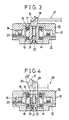
- An optical scanning system in a first embodiment according to the present invention will be described hereinafter with reference to Figs. 1 to 3.
- An optical scanning system 11 is provided with a motor 12 comprising a stator 13 having a boss 14, a rotor 16 supported for rotation by bearings 15 on the boss 14 of the stator 13.
- the rotor 16 has a hollow output shaft 17 internally defining a space for containing parts.
- a reflecting mirror 19, i.e., a light deflecting member, having a reflecting surface 18 inclined at an angle of 45° to the center of rotation is attached to the upper end of the output shaft 17.
- a lens barrel 20 is set upright on the bottom of the stator 13 so as to extend in the bore of the output shaft 17.
- a collimator lens 21 is attached to the upper end of the lens barrel 20, and a semiconductor laser 22 is attached to the lower end of the lens barrel 20.
- Coils 23 are provided on the flange of the stator 13, and magnets 24 are attached to the inner surface of the rotor 16 opposite to the coils 23.
- the rotor 16 holding the reflecting mirror 19 is rotated by magnetic motive force generated by the interaction between the coils 23 and the magnets 24.
- Laser light rays emitted by the semiconductor laser 22 are collimated by the collimator lens 21 to produce a scanning laser light beam.
- the scanning laser light beam falls on the rotating reflecting surface 18 of the reflecting mirror 19 and is deflected to sweep a target surface for scanning. Since the center of rotation of the reflecting mirror 19 and the optical axis of the semiconductor laser 22 are aligned, the scanning laser light beam is not deflected in the feed direction. Since the optical path between the semiconductor laser 22 and the reflecting mirror 19 extends within the output shaft 17 of the motor 12, the optical scanning system 11 can be constructed in a very compact construction.
- the reflecting mirror 19 of the optical scanning system may be substituted by a prism 26 (Fig. 2) having a reflecting surface 25 inclined at an angle of 45° to the optical path.
- the collimator lens 21 of the optical scanning system 11 in this embodiment is disposed between the semiconductor laser 22 and the reflecting mirror 19 and is fixed to the lens barrel 20 set upright on the stator 13 so as to extend within the output shaft 17 of the motor 12, the present invention is not limited to such a construction.
- An optical scanning system 27 in a modification of the optical scanning system 11 may be provided with the collimator lens 21 provided within the bore of the output shaft 17 of the rotor 16 of the motor 12 and attached directly to the output shaft 17.
- the optical scanning system 27 need not be provided with the lens barrel 20 and is simpler in construction, more compact and lighter than the optical scanning system 11.
- the optical scanning system 28 comprises a motor 12 having a stator 13 and a rotor 16, a pentaprism 31 having two reflecting surfaces 29 and 30 including an angle of 45° and attached to the upper surface of the rotor 16 of the motor 12, a semiconductor laser 22 provided on the bottom of the stator 13, a lens barrel 20 set upright on the stator 13, and a collimator lens 21 fitted in a lens barrel 20.
- Laser light rays emitted by the semiconductor laser 22 are collimated in a scanning laser beam by the collimator lens 21, the scanning laser beam falls on the pentaprism 31 rotating together with the rotor 16. Then, the scanning laser beam is reflected sequentially by the reflecting surfaces 29 and 30 of the pentaprism 31 so as to sweep a target surface for scanning.
- the direction of travel of the scanning laser beam reflected by the reflecting mirror 19 of the optical scanning system 11 in the first embodiment varies as shown in Fig. 5 when the inclination of the reflecting mirror 19 with respect to the optical path varies due to the runout of the rotor 16
- the direction of travel of the scanning laser beam reflected by the two reflecting surfaces 29 and 30 of the pentaprism 31 of the optical scanning system 28 in the second embodiment remains constant as shown in Figs. 6(a), 6(b) and 6(c) even if the angular position of the pentaprism 31 varies.
- the direction of travel of the scanning laser beam reflected through an angle of 90° by the two reflecting surfaces 29 and 30 of the pentaprism 31 is not deviated in the feed direction by the tilt of the pentaprism 31. Accordingly, the optical scanning system 28 executes scanning operation by using a scanning laser beam having satisfactory optical characteristics without requiring any correcting optical system, and the scanning laser beam remains stable regardless of the runout of the rotor 16.
- the pentaprism 31 having the two reflecting surfaces 29 and 30 including an angle of 45° employed in the optical scanning system 28 may be substituted by two reflecting mirrors disposed so as to include an angle of 45°.
- the optical scanning system 52 comprises a motor 53 having a rotor 54 provided with a bore, a prism 55 having a reflecting surface 56 inclined at an angle of 45° to the center of rotation of the rotor 54 and attached to the upper surface of the rotor 54, a collimator lens 57 fitted in the bore of the rotor 54, a semiconductor laser 58 disposed opposite to the collimator lens 57, an aperture 61, and a meniscus lens 62, i.e., a correcting optical means.
- the aperture 61 and the meniscus lens 62 are arranged in that order on a scanning optical path between the reflecting surface 56 of the prism 55 and a circumference 60, i.e., a target surface, of a photoconductive drum 59.
- the meniscus lens 62 has a concave surface 63 of a radius R in of curvature on which the laser light beam falls and a convex surface 64 of a radius R out of curvature from which the laser light beam emerges.
- the radii R in and R out meet the following relation: 0.9 ⁇ R in /R out ⁇ 1.1
- the meniscus lens 62 has a focal length ⁇ of 780 mm and is formed of BK-7 having a refractive index n of 1.51143. As shown in Fig. 7, the distance between the optical center of the concave surface 63 of a radius R in of curvature in the range of 8 to 20 mm and a reflection point 65 on the reflecting surface 56 of the prism 55 is in the range of 5 to 10 mm.
- the collimator lens 57 collimates rays of laser light emitted by the semiconductor laser 58 in a laser light beam
- the reflecting surface 56 of the prism 55 rotating together with the rotor 54 of the motor 53 reflects the laser light beam for scanning
- the aperture 61 limits the sweep angle ⁇ of the scanning laser light beam and shapes the scanning laser light beam.
- the meniscus lens 62 corrects the curvature of image field before the scanning laser light beam sweeps the target surface 60 of the photoconductive drum 59 for scanning.
- the disposition of the meniscus lens 62 having the concave surface 63 and the convex surface 64, which are substantially the same in radius of curvature and have comparatively large curvatures, close to the prism 55 enables the optical scanning system 52 comprising the motor 53 and the meniscus lens 62 to be constructed in a very compact construction, limits the curvature of image field to a very small degree and provides the optical scanning system with satisfactory optical characteristics.
- optical characteristics of the optical scanning system 52 were evaluated in terms of curvature of image field with respect to a scanning direction and curvature of image field with respect to a feed direction as evaluation functions, and values of the parameters that make the curvatures of image field with respect to a scanning direction and with respect to a feed direction approach infinitesimals were determined through simulation.
- t (mm) is the thickness of the meniscus lens 62 along the optical axis
- ⁇ (degree) is scanning angle
- R in (mm) is the radius of curvature of the concave surface 63 of the meniscus lens 62
- R out (mm) is the radius of curvature of the convex surface 64 of the meniscus lens 62
- a (mm) is the distance between the reflecting point 65 and the optical center of the concave surface 63 of the meniscus lens 62
- L is the distance between the reflecting point 65 and the target surface 60.
- the optical scanning system 52 scans the target surface 60 of the photoconductive drum 59 by the scanning laser light beam having satisfactory optical characteristics and a minute curvature of image field and, consequently, an image can be printed in a very good print quality.
- the f ⁇ error in the operation of the optical scanning system 52 can readily be corrected by controlling the timing of driving the semiconductor laser 58 without requiring optical correction.
- the optical scanning system 52 comprising the motor 53 and the meniscus lens 62 can be constructed in a compact, lightweight construction, and the parts can easily be assembled in a unit, which improves the productivity of a production line for producing an equipment incorporating the radical scanning system 52.
- the laser light beam emitted by the semiconductor laser 58 having a vertical divergence ratio and a horizontal divergence ratio which is different from the vertical divergence ratio is shaped by the aperture 61.
- a cylindrical lens may be employed to shape the laser light beam by the refractive function of the cylindrical lens to improve the light intensity distribution of the laser light beam.
- an aperture having a large NA (numerical aperture) to screen stray light so that the stray light may not interfere with the scanning light beam.
Abstract
Description
- The present invention relates to an optical scanning system to be incorporated into an electrophotographic apparatus or a bar-code scanner.
- Electrophotography capable of printing in a high print quality has recently been developed. Electrophotography employs an optical scanning system to form an image. The optical scanning system has a light deflecting member mounted on the output shaft of a motor and disposed on the passage of a light beam emitted by a light source, such as a semiconductor laser. The light reflecting member reflects the light beam on an image plane, such as a photoconductive surface or a surface marked with a bar code. A polygonal rotating mirror when used as the light deflecting member is capable of reflecting light beams by its plurality of reflecting surfaces at a high frequency. However, it is difficult to correct the inevitable difference in characteristics between the plurality of reflecting surfaces. Furthermore, it is difficult to construct the optical scanning system employing a polygonal rotating mirror in a compact construction because optical parts including a semiconductor laser and a collimator lens must be arranged near the motor for rotating the polygonal rotating mirror.
- Figs. 10 and 11 show an optical scanning system incorporating improvements to solve those problems disclosed in Japanese Patent Laid-open No. 62-257119. Referring to Figs. 10 and 11, this known optical scanning system 1 has a
transparent member 2, i.e., a light deflecting member, attached to the output shaft of a motor, not shown. One end of thetransparent member 2 is cut diagonally to form a reflectingsurface 3 inclined at an angle of 45° to the axis of thetransparent member 2. A portion of the circumference of thetransparent member 2 extending at an acute angle, i.e., 45°, to the reflectingsurface 3 is formed in a cylindroid surface 4. As shown in Figs. 10 and 11, the center of rotation of thetransparent member 2 is dislocated from the optical axis of a laser light source, not shown, for the layout of other parts and optical paths. - A scanning light beam traveling along the axis of the
transparent member 2 falls on the reflectingsurface 3 of the rotatingtransparent member 2, and the scanning light beam is reflected by the reflectingsurface 3 for scanning. The scanning light beam reflected by the reflectingsurface 3 is refracted at the cylindroid surface 4. Optical scanning systems employing a polygonal rotating mirror as a light deflecting member are classified into those of a postobjective type and those of a preobjective type. An optical scanning system employing a light deflecting member having a reflecting surface wich receives a light beam along an optical path inclined to the center of rotation of the reflecting surface needs a correcting optical system because such an optical scanning system causes aberration, such as the curvature of image field. The optical scanning system 1 corrects the aberration of the scanning light beam reflected by the reflectingsurface 3 by the refractive power of the cylindroid surface 4. - Figs. 12 and 13 show another known optical scanning system disclosed in Japanese Patent Laid-open No. 1-283512. Referring to Figs. 12 and 13, this known
optical scanning system 5 employs a reflectingmirror 7, i.e., a light deflecting member, having a reflectingsurface 6 inclined at an angle of 45° to its axis. The reflectingmirror 7 is attached to the output shaft of amotor 8. A tubular member 9 provided with aslit 10 in its circumference at a position corresponding to the reflectingsurface 6 is attached to the upper surface of themotor 8 so as to enclose the reflectingmirror 7. A laser light source, not shown, is disposed on the axis of themotor 8 opposite to the upper open end of the tubular member 9. - A scanning light beam that falls on the reflecting
mirror 7 along the axis of the reflectingmirror 7 is reflected by thereflecting surface 6 and travels through theslit 10 of the tubular member 9. The shape of the scanning light beam is shaped by theslit 10. - If the reflecting
surface 6 is flat, fϑ error and aberration, such as the curvature of image field, occur inevitably in the scanning light beam. Therefore, theoptical scanning system 5 needs means for correcting the fϑ error and the aberration. - Fig. 14 shows an optical scanning system incorporating improvements for correcting fϑ error and aberration disclosed in Japanese Patent Laid-open No. 62-138823. Referring to Fig. 14, this known
optical scanning system 41 has a polygonal rotatingmirror 42 attached to the output shaft of a motor, not shown, and disposed so that its reflecting surfaces move across a narrow light beam, and anaspherical lens 44, i.e., a correcting optical element, disposed on the optical path of the reflected light beam between the polygonalrotating mirror 42 and atarget surface 43. As shown in Fig. 14, theaspherical lens 44 has a substantially W-shaped light receiving surface and a convex light emitting surface. - The
aspherical lens 44 corrects the fϑ error and curvature of image field of the scanning light beam reflected by the reflecting surface of the polygonal rotatingmirror 42 and focuses the scanning light beam on thetarget surface 43. - It is a first object of the present invention to provide an optical scanning system of a simple, compact construction comprising: a motor having a space for containing parts; and a light deflecting member attached to the output shaft of the motor; characterized in that an optical path extends through the output shaft of the motor between a semiconductor laser and the light deflecting member, and at least a collimator lens is provided in the space for containing parts of the motor.
- A second object of the present invention is to dispose the light deflecting member with its center of rotation in alignment with the optical axis of the semiconductor laser.
- A third object of the present invention is to provide an optical scanning system employing a light deflecting member, and capable of preventing the change of the direction of travel of a reflected light beam even if the angular position of the light deflecting member varies due to errors introduced into the parts during manufacture and of preventing the deviation of the scanning light beam in the direction of feed due to the misalignment of the light deflecting member.
- A fourth object of the present invention is to provide a compact, lightweight optical scanning system comprising: a light deflecting member; and a meniscus lens having a concave surface having a large curvature disposed close to the light deflecting member to limit the curvature of image field of the scanning light beam to a very small degree.
- A fifth object of the present invention is to provide an optical scanning system of a simple construction employing a meniscus lens having a convex surface and a concave surface of a curvature substantially equal to that of the convex surface to limit the curvature of image field of the scanning light beam to a very small degree.
-
- Figure 1 is a longitudinal sectional view of an optical scanning system in a first embodiment according to the present invention;
- Figure 2 is a side view of an essential portion of a modification of the optical scanning system of Fig. 1;
- Figure 3 is a longitudinal sectional view of another modification of the optical scanning system of Fig. 1;
- Figure 4 is a longitudinal sectional view of an optical scanning system in a second embodiment according to the present invention;
- Figures 5, 6(a), 6(b) and 6(c) are diagrams of assistance in explaining optical characteristics;
- Figure 7 is a plan view of an optical scanning system in a third embodiment according to the present invention;
- Figure 8 is a longitudinal sectional view of the optical scanning system of Fig. 7;
- Figure 9 is a plan view of an essential portion of the optical scanning system of Fig. 7;
- Figure 10 is a side view of a first conventional optical system;
- Figure 11 is a plan view of the conventional optical system of Fig. 10;
- Figure 12 is a perspective view of a second conventional optical system;
- Figure 13 is a longitudinal sectional view of the conventional optical scanning system of Fig. 12; and
- Figure 14 is a side view of a third conventional optical scanning system.
- An optical scanning system in a first embodiment according to the present invention will be described hereinafter with reference to Figs. 1 to 3. An
optical scanning system 11 is provided with amotor 12 comprising astator 13 having aboss 14, arotor 16 supported for rotation bybearings 15 on theboss 14 of thestator 13. Therotor 16 has ahollow output shaft 17 internally defining a space for containing parts. A reflectingmirror 19, i.e., a light deflecting member, having a reflectingsurface 18 inclined at an angle of 45° to the center of rotation is attached to the upper end of theoutput shaft 17. Alens barrel 20 is set upright on the bottom of thestator 13 so as to extend in the bore of theoutput shaft 17. Acollimator lens 21 is attached to the upper end of thelens barrel 20, and asemiconductor laser 22 is attached to the lower end of thelens barrel 20.Coils 23 are provided on the flange of thestator 13, andmagnets 24 are attached to the inner surface of therotor 16 opposite to thecoils 23. - The
rotor 16 holding the reflectingmirror 19 is rotated by magnetic motive force generated by the interaction between thecoils 23 and themagnets 24. Laser light rays emitted by thesemiconductor laser 22 are collimated by thecollimator lens 21 to produce a scanning laser light beam. The scanning laser light beam falls on the rotating reflectingsurface 18 of the reflectingmirror 19 and is deflected to sweep a target surface for scanning. Since the center of rotation of the reflectingmirror 19 and the optical axis of thesemiconductor laser 22 are aligned, the scanning laser light beam is not deflected in the feed direction. Since the optical path between thesemiconductor laser 22 and the reflectingmirror 19 extends within theoutput shaft 17 of themotor 12, theoptical scanning system 11 can be constructed in a very compact construction. - In a modification, the reflecting
mirror 19 of the optical scanning system may be substituted by a prism 26 (Fig. 2) having a reflectingsurface 25 inclined at an angle of 45° to the optical path. - Although the
collimator lens 21 of theoptical scanning system 11 in this embodiment is disposed between thesemiconductor laser 22 and the reflectingmirror 19 and is fixed to thelens barrel 20 set upright on thestator 13 so as to extend within theoutput shaft 17 of themotor 12, the present invention is not limited to such a construction. Anoptical scanning system 27 in a modification of theoptical scanning system 11 may be provided with thecollimator lens 21 provided within the bore of theoutput shaft 17 of therotor 16 of themotor 12 and attached directly to theoutput shaft 17. Theoptical scanning system 27 need not be provided with thelens barrel 20 and is simpler in construction, more compact and lighter than theoptical scanning system 11. - An
optical scanning system 28 in a second embodiment according to the present invention will be described hereinafter with reference to Figs. 4, 5, 6(a), 6(b) and 6(c). Theoptical scanning system 28 comprises amotor 12 having astator 13 and arotor 16, apentaprism 31 having two reflectingsurfaces rotor 16 of themotor 12, asemiconductor laser 22 provided on the bottom of thestator 13, alens barrel 20 set upright on thestator 13, and acollimator lens 21 fitted in alens barrel 20. Laser light rays emitted by thesemiconductor laser 22 are collimated in a scanning laser beam by thecollimator lens 21, the scanning laser beam falls on thepentaprism 31 rotating together with therotor 16. Then, the scanning laser beam is reflected sequentially by the reflectingsurfaces pentaprism 31 so as to sweep a target surface for scanning. - Although the direction of travel of the scanning laser beam reflected by the reflecting
mirror 19 of theoptical scanning system 11 in the first embodiment varies as shown in Fig. 5 when the inclination of the reflectingmirror 19 with respect to the optical path varies due to the runout of therotor 16, the direction of travel of the scanning laser beam reflected by the two reflectingsurfaces pentaprism 31 of theoptical scanning system 28 in the second embodiment remains constant as shown in Figs. 6(a), 6(b) and 6(c) even if the angular position of thepentaprism 31 varies. Furthermore, the direction of travel of the scanning laser beam reflected through an angle of 90° by the two reflectingsurfaces pentaprism 31 is not deviated in the feed direction by the tilt of thepentaprism 31. Accordingly, theoptical scanning system 28 executes scanning operation by using a scanning laser beam having satisfactory optical characteristics without requiring any correcting optical system, and the scanning laser beam remains stable regardless of the runout of therotor 16. - The
pentaprism 31 having the two reflectingsurfaces optical scanning system 28 may be substituted by two reflecting mirrors disposed so as to include an angle of 45°. - An
optical scanning system 52 in a third embodiment according to the present invention will be described hereinafter with reference to Figs. 7 to 9. As shown in Fig. 8, theoptical scanning system 52 comprises amotor 53 having arotor 54 provided with a bore, aprism 55 having a reflectingsurface 56 inclined at an angle of 45° to the center of rotation of therotor 54 and attached to the upper surface of therotor 54, acollimator lens 57 fitted in the bore of therotor 54, asemiconductor laser 58 disposed opposite to thecollimator lens 57, anaperture 61, and ameniscus lens 62, i.e., a correcting optical means. Theaperture 61 and themeniscus lens 62 are arranged in that order on a scanning optical path between the reflectingsurface 56 of theprism 55 and acircumference 60, i.e., a target surface, of aphotoconductive drum 59. As shown in Fig. 9, themeniscus lens 62 has aconcave surface 63 of a radius Rin of curvature on which the laser light beam falls and aconvex surface 64 of a radius Rout of curvature from which the laser light beam emerges. The radii Rin and Rout meet the following relation:
- The
meniscus lens 62 has a focal length λ of 780 mm and is formed of BK-7 having a refractive index n of 1.51143. As shown in Fig. 7, the distance between the optical center of theconcave surface 63 of a radius Rin of curvature in the range of 8 to 20 mm and areflection point 65 on the reflectingsurface 56 of theprism 55 is in the range of 5 to 10 mm. - The
collimator lens 57 collimates rays of laser light emitted by thesemiconductor laser 58 in a laser light beam, the reflectingsurface 56 of theprism 55 rotating together with therotor 54 of themotor 53 reflects the laser light beam for scanning, and theaperture 61 limits the sweep angle ϑ of the scanning laser light beam and shapes the scanning laser light beam. Then, themeniscus lens 62 corrects the curvature of image field before the scanning laser light beam sweeps thetarget surface 60 of thephotoconductive drum 59 for scanning. - The disposition of the
meniscus lens 62 having theconcave surface 63 and theconvex surface 64, which are substantially the same in radius of curvature and have comparatively large curvatures, close to theprism 55 enables theoptical scanning system 52 comprising themotor 53 and themeniscus lens 62 to be constructed in a very compact construction, limits the curvature of image field to a very small degree and provides the optical scanning system with satisfactory optical characteristics. - The optical characteristics of the
optical scanning system 52 were evaluated in terms of curvature of image field with respect to a scanning direction and curvature of image field with respect to a feed direction as evaluation functions, and values of the parameters that make the curvatures of image field with respect to a scanning direction and with respect to a feed direction approach infinitesimals were determined through simulation. The results of simulation are shown in Tables 1 and 2, in which t (mm) is the thickness of themeniscus lens 62 along the optical axis, ϑ (degree) is scanning angle, Rin (mm) is the radius of curvature of theconcave surface 63 of themeniscus lens 62, Rout (mm) is the radius of curvature of theconvex surface 64 of themeniscus lens 62, a (mm) is the distance between the reflectingpoint 65 and the optical center of theconcave surface 63 of themeniscus lens 62, and L is the distance between the reflectingpoint 65 and thetarget surface 60. - Results of simulation using the
meniscus lens 62 having theconcave surface 63 and theconvex surface 64 having the same radius R of curvature are shown in Table 2. - As is obvious from Tables 1 and 2, the use of the
meniscus lens 62 having theconcave surface 63 having a large radius of curvature in the range of 8 to 20 mm, meeting the relation between the radius Rin of curvature of theconcave surface 63 and the radius Rout of curvature of theconvex surface 64, the same expressed by: 0.9 ≦ Rin/Rout < 1.1, and disposed close to theprism 55 so that the distance between the reflectingpoint 65 on the reflectingsurface 56 of theprism 55 and the optical center of theconcave surface 63 is in the range of 5 to 10 mm, limits curvatures of image field with respect to the scanning direction and with respect to the feed direction to a very small degree. - Thus, the
optical scanning system 52 scans thetarget surface 60 of thephotoconductive drum 59 by the scanning laser light beam having satisfactory optical characteristics and a minute curvature of image field and, consequently, an image can be printed in a very good print quality. The fϑ error in the operation of theoptical scanning system 52 can readily be corrected by controlling the timing of driving thesemiconductor laser 58 without requiring optical correction. - Since the comparatively
small meniscus lens 62 having a large radius of curvature is disposed close to theprism 55, theoptical scanning system 52 comprising themotor 53 and themeniscus lens 62 can be constructed in a compact, lightweight construction, and the parts can easily be assembled in a unit, which improves the productivity of a production line for producing an equipment incorporating theradical scanning system 52. - In this embodiment, the laser light beam emitted by the
semiconductor laser 58, having a vertical divergence ratio and a horizontal divergence ratio which is different from the vertical divergence ratio is shaped by theaperture 61. In a modification, a cylindrical lens may be employed to shape the laser light beam by the refractive function of the cylindrical lens to improve the light intensity distribution of the laser light beam. When a cylindrical lens is employed for beam shaping, an aperture having a large NA (numerical aperture) to screen stray light so that the stray light may not interfere with the scanning light beam. Furthermore, it is possible to provide theoptical scanning system 52 with, for example, a polygonal rotating mirror of dimensions corresponding to the foregoing dimensions instead of theprism 55.
Claims (5)
- An optical scanning system comprising: a motor having an output shaft; a light deflecting member attached to the output shaft of said motor; a semiconductor laser; and a collimator lens disposed between said light deflecting member and said semiconductor laser with its optical axis in alignment with the optical axis of said semiconductor laser; characterized in that a space for containing parts is formed in the output shaft of said motor, said light deflecting member is attached to one end of the output shaft of said motor, an optical path extends through the space formed in the output shaft of said motor between said semiconductor laser and said light deflecting member, and said collimator lens is disposed in the space formed in the output shaft of said motor.
- An optical scanning system according to Claim 1, wherein the output shaft of said motor is a hollow shaft forming the space for containing parts.
- An optical scanning system according to Claim 1, wherein said light deflecting member has two reflecting surfaces formed so as to include an angle of 45°.
- An optical scanning system according to Claim 1, wherein said light deflecting member attached to the output shaft of said motor is disposed on the optical axis of said semiconductor laser after said collimator lens with respect to the direction of travel of a laser light beam emitted by said semiconductor laser, said light deflecting member has at least one flat reflecting surface, a correcting optical system is provided on an optical path between the flat reflecting surface of said light deflecting member and a target surface to be scanned, and the correcting optical system comprises a meniscus lens having a concave surface of a radius of curvature in the range of 8 to 20 mm and disposed with the concave surface facing the light deflecting member so that the distance between the reflecting point of said light deflecting member and the optical center of the concave surface is in the range of 5 to 10 mm.
- An optical scanning system according to Claim 4, wherein the meniscus lens meets a relation represented by:

Applications Claiming Priority (4)
| Application Number | Priority Date | Filing Date | Title |
|---|---|---|---|
| JP88448/90 | 1990-04-03 | ||
| JP2088448A JP2690591B2 (en) | 1990-04-03 | 1990-04-03 | Optical scanning device |
| JP73192/90U | 1990-07-10 | ||
| JP1990073192U JPH0431114U (en) | 1990-07-10 | 1990-07-10 |
Publications (3)
| Publication Number | Publication Date |
|---|---|
| EP0450901A2 true EP0450901A2 (en) | 1991-10-09 |
| EP0450901A3 EP0450901A3 (en) | 1992-04-29 |
| EP0450901B1 EP0450901B1 (en) | 1994-10-26 |
Family
ID=26414341
Family Applications (1)
| Application Number | Title | Priority Date | Filing Date |
|---|---|---|---|
| EP91302859A Expired - Lifetime EP0450901B1 (en) | 1990-04-03 | 1991-04-02 | Optical scanning system |
Country Status (4)
| Country | Link |
|---|---|
| US (1) | US5184245A (en) |
| EP (1) | EP0450901B1 (en) |
| KR (1) | KR940002358B1 (en) |
| DE (1) | DE69104762T2 (en) |
Cited By (6)
| Publication number | Priority date | Publication date | Assignee | Title |
|---|---|---|---|---|
| EP0566155A1 (en) * | 1992-04-17 | 1993-10-20 | Kabushiki Kaisha TEC | Optical scanning device for scanning laser beam focused on image-forming surfaces |
| WO1996035211A1 (en) * | 1995-04-29 | 1996-11-07 | Linotype-Hell Ag | Light beam deflecting device |
| US5768001A (en) * | 1996-06-10 | 1998-06-16 | Agfa Division, Bayer Corp. | Rotating beam deflector having an integral wave front correction element |
| WO1998047036A1 (en) * | 1997-04-11 | 1998-10-22 | Geoffrey Owen | Beam expander, optical deflector, beam splitter and scanner |
| CN108988565A (en) * | 2017-05-30 | 2018-12-11 | 日本电产株式会社 | Rotation drive device |
| EP4109142A1 (en) | 2021-06-25 | 2022-12-28 | Friedrich-Alexander-Universität Erlangen-Nürnberg | Light sheet imaging device, scanner for a light sheet imaging device and method of operating a light sheet imaging device |
Families Citing this family (19)
| Publication number | Priority date | Publication date | Assignee | Title |
|---|---|---|---|---|
| US5325116A (en) * | 1992-09-18 | 1994-06-28 | Texas Instruments Incorporated | Device for writing to and reading from optical storage media |
| JPH0743672A (en) * | 1993-08-02 | 1995-02-14 | Sony Corp | Optical element turning device, solenoid and liquid crystal projector |
| US5583684A (en) * | 1995-06-06 | 1996-12-10 | Spot Technology Inc. | Lens assembly fixing device of scanner |
| JPH10238535A (en) * | 1997-02-27 | 1998-09-08 | Nippon Seiko Kk | Spindle motor for disc |
| US7518804B2 (en) * | 2003-04-24 | 2009-04-14 | Bae Systems Information And Electronic Systems Integration Inc. | Singlet telescopes with controllable ghosts for laser beam forming |
| KR100803591B1 (en) * | 2004-10-14 | 2008-02-19 | 삼성전자주식회사 | Mirror positioning structure of laser scanning unit and laser scanning unit employing the mirror positioning structure |
| JP5099020B2 (en) * | 2009-01-21 | 2012-12-12 | セイコーエプソン株式会社 | Optical scanning apparatus and image forming apparatus |
| CN103212795B (en) * | 2013-02-04 | 2015-08-19 | 张立国 | A kind of laser beam whirligig based on hollow electric spindle |
| US9310609B2 (en) | 2014-07-25 | 2016-04-12 | Hand Held Products, Inc. | Axially reinforced flexible scan element |
| KR102399590B1 (en) * | 2015-02-04 | 2022-05-19 | 삼성전자주식회사 | Driving module for lens |
| CN105785383B (en) * | 2016-05-19 | 2019-01-08 | 上海思岚科技有限公司 | A kind of laser scanning range-finding device |
| CN106514673A (en) * | 2016-12-30 | 2017-03-22 | 上海木爷机器人技术有限公司 | Obstacle detecting device, robot and obstacle detecting method |
| JP2018120159A (en) * | 2017-01-27 | 2018-08-02 | 日本電産株式会社 | Rotary driving device and method of manufacturing rotary driving device |
| JP2018207575A (en) * | 2017-05-30 | 2018-12-27 | 日本電産株式会社 | Rotary drive device |
| JP2019012104A (en) * | 2017-06-29 | 2019-01-24 | 日本電産株式会社 | Housing and housing unit |
| US20190094527A1 (en) * | 2017-09-28 | 2019-03-28 | Nidec Corporation | Rotary drive apparatus |
| US10852534B2 (en) * | 2018-04-26 | 2020-12-01 | Faro Technologies, Inc. | Mirror assemblies for imaging devices |
| CN109375192A (en) * | 2018-12-12 | 2019-02-22 | 广州维思车用部件有限公司 | Automated driving system, laser radar and its Laser emission structure |
| WO2021128023A1 (en) * | 2019-12-24 | 2021-07-01 | 深圳市大疆创新科技有限公司 | Driving electric motor, scanning module, and laser radar |
Citations (4)
| Publication number | Priority date | Publication date | Assignee | Title |
|---|---|---|---|---|
| US3093736A (en) * | 1959-12-21 | 1963-06-11 | Perkin Elmer Corp | Multiple prism optical scanner |
| US3961838A (en) * | 1975-01-10 | 1976-06-08 | Zygo Corporation | Apparatus for producing a scanning laser beam of constant linear velocity |
| DE2449259B2 (en) * | 1973-10-16 | 1976-09-16 | AGA AB, Lidingö (Schweden) | OPTICAL ORIENTATION DEVICE |
| US4010361A (en) * | 1975-03-03 | 1977-03-01 | Latterman Robert C | Light deflection apparatus |
Family Cites Families (12)
| Publication number | Priority date | Publication date | Assignee | Title |
|---|---|---|---|---|
| FR1475008A (en) * | 1966-02-18 | 1967-03-31 | Philips Massiot Mat Medic | Camera scanning device |
| US3588249A (en) * | 1968-06-17 | 1971-06-28 | Robert H Studebaker | Laser beam survey apparatus |
| JPS60159417A (en) * | 1984-01-31 | 1985-08-20 | Matsushita Electric Ind Co Ltd | Fluid bearing device |
| JPH0226215Y2 (en) * | 1984-12-07 | 1990-07-17 | ||
| JPS61239211A (en) * | 1985-04-16 | 1986-10-24 | Dainippon Screen Mfg Co Ltd | Optical beam scanner incorporating light source |
| DE3687932T2 (en) * | 1985-07-23 | 1993-09-30 | Kanegafuchi Chemical Ind | Laser scanning motor and its manufacture. |
| JPS6294814A (en) * | 1985-10-20 | 1987-05-01 | Ricoh Co Ltd | Ball bearing type optical deflector |
| JPS62138823A (en) * | 1985-12-12 | 1987-06-22 | Seiko Epson Corp | Photoscanning device |
| US4699447A (en) * | 1986-02-27 | 1987-10-13 | Spectra-Physics, Inc. | Optical beam scanner with rotating mirror |
| JPS62257119A (en) * | 1986-04-30 | 1987-11-09 | Ricoh Co Ltd | Optical scanning device |
| JP2869064B2 (en) * | 1987-03-11 | 1999-03-10 | ソニー株式会社 | Disk drive |
| JPH01283512A (en) * | 1988-05-11 | 1989-11-15 | Ricoh Co Ltd | Image forming device |
-
1991
- 1991-03-29 KR KR1019910005018A patent/KR940002358B1/en not_active IP Right Cessation
- 1991-04-02 EP EP91302859A patent/EP0450901B1/en not_active Expired - Lifetime
- 1991-04-02 DE DE69104762T patent/DE69104762T2/en not_active Expired - Fee Related
- 1991-04-03 US US07/680,132 patent/US5184245A/en not_active Expired - Fee Related
Patent Citations (4)
| Publication number | Priority date | Publication date | Assignee | Title |
|---|---|---|---|---|
| US3093736A (en) * | 1959-12-21 | 1963-06-11 | Perkin Elmer Corp | Multiple prism optical scanner |
| DE2449259B2 (en) * | 1973-10-16 | 1976-09-16 | AGA AB, Lidingö (Schweden) | OPTICAL ORIENTATION DEVICE |
| US3961838A (en) * | 1975-01-10 | 1976-06-08 | Zygo Corporation | Apparatus for producing a scanning laser beam of constant linear velocity |
| US4010361A (en) * | 1975-03-03 | 1977-03-01 | Latterman Robert C | Light deflection apparatus |
Cited By (8)
| Publication number | Priority date | Publication date | Assignee | Title |
|---|---|---|---|---|
| EP0566155A1 (en) * | 1992-04-17 | 1993-10-20 | Kabushiki Kaisha TEC | Optical scanning device for scanning laser beam focused on image-forming surfaces |
| US5402258A (en) * | 1992-04-17 | 1995-03-28 | Tokyo Electric Co., Ltd. | Optical scanning device for scanning laser beam focused on image-forming surface |
| WO1996035211A1 (en) * | 1995-04-29 | 1996-11-07 | Linotype-Hell Ag | Light beam deflecting device |
| US5877887A (en) * | 1995-04-29 | 1999-03-02 | Linotype-Hell Ag | Light beam deflection means |
| US5768001A (en) * | 1996-06-10 | 1998-06-16 | Agfa Division, Bayer Corp. | Rotating beam deflector having an integral wave front correction element |
| WO1998047036A1 (en) * | 1997-04-11 | 1998-10-22 | Geoffrey Owen | Beam expander, optical deflector, beam splitter and scanner |
| CN108988565A (en) * | 2017-05-30 | 2018-12-11 | 日本电产株式会社 | Rotation drive device |
| EP4109142A1 (en) | 2021-06-25 | 2022-12-28 | Friedrich-Alexander-Universität Erlangen-Nürnberg | Light sheet imaging device, scanner for a light sheet imaging device and method of operating a light sheet imaging device |
Also Published As
| Publication number | Publication date |
|---|---|
| EP0450901B1 (en) | 1994-10-26 |
| US5184245A (en) | 1993-02-02 |
| KR940002358B1 (en) | 1994-03-23 |
| DE69104762T2 (en) | 1995-05-24 |
| EP0450901A3 (en) | 1992-04-29 |
| DE69104762D1 (en) | 1994-12-01 |
| KR910018863A (en) | 1991-11-30 |
Similar Documents
| Publication | Publication Date | Title |
|---|---|---|
| EP0450901B1 (en) | Optical scanning system | |
| US4962983A (en) | Laser optical apparatus | |
| US20010053014A1 (en) | Scanning image forming lens and optical scanning apparatus | |
| US20220075181A1 (en) | Optical scanner and electrophotographic image forming apparatus | |
| US4804981A (en) | Aspheric lens for polygon mirror tilt error correction and scan bow correction in an electrophotographic printer | |
| US5801746A (en) | Image forming apparatus having a plurality of mirror members each capable of moving in a parallel or rotary direction | |
| US4984858A (en) | Light beam scanning optical system | |
| KR100335624B1 (en) | Laser beam scanning apparatus | |
| US6888655B2 (en) | Optical beam scanning device | |
| JPH09211352A (en) | Scanning optical device | |
| US6933961B2 (en) | Optical scanning system | |
| US7023597B2 (en) | Optical scanning device, image reading device provided with this, image forming device, and photographing device | |
| US5966232A (en) | Scanning optical system | |
| EP0523320A1 (en) | Optical unit for use in laser beam printer apparatus | |
| US6956686B2 (en) | Scanning optical system | |
| US6670980B1 (en) | Light-scanning optical system | |
| US20020122234A1 (en) | Scanning optical system | |
| JPH08248345A (en) | Optical scanner | |
| KR100601648B1 (en) | Optical scanning unit | |
| JPH03287220A (en) | Optical scanning device | |
| JP2773593B2 (en) | Light beam scanning optical system | |
| US20030066888A1 (en) | Optical scanner and image forming apparatus | |
| KR100335625B1 (en) | Laser beam scanning device | |
| JP3110816B2 (en) | Optical scanning device | |
| JP2907292B2 (en) | Achromatic laser scanning optics |
Legal Events
| Date | Code | Title | Description |
|---|---|---|---|
| PUAI | Public reference made under article 153(3) epc to a published international application that has entered the european phase |
Free format text: ORIGINAL CODE: 0009012 |
|
| 17P | Request for examination filed |
Effective date: 19910410 |
|
| AK | Designated contracting states |
Kind code of ref document: A2 Designated state(s): DE FR GB |
|
| PUAL | Search report despatched |
Free format text: ORIGINAL CODE: 0009013 |
|
| AK | Designated contracting states |
Kind code of ref document: A3 Designated state(s): DE FR GB |
|
| 17Q | First examination report despatched |
Effective date: 19940111 |
|
| GRAA | (expected) grant |
Free format text: ORIGINAL CODE: 0009210 |
|
| AK | Designated contracting states |
Kind code of ref document: B1 Designated state(s): DE FR GB |
|
| REF | Corresponds to: |
Ref document number: 69104762 Country of ref document: DE Date of ref document: 19941201 |
|
| ET | Fr: translation filed | ||
| PLBE | No opposition filed within time limit |
Free format text: ORIGINAL CODE: 0009261 |
|
| STAA | Information on the status of an ep patent application or granted ep patent |
Free format text: STATUS: NO OPPOSITION FILED WITHIN TIME LIMIT |
|
| 26N | No opposition filed | ||
| PGFP | Annual fee paid to national office [announced via postgrant information from national office to epo] |
Ref country code: DE Payment date: 20010326 Year of fee payment: 11 |
|
| PGFP | Annual fee paid to national office [announced via postgrant information from national office to epo] |
Ref country code: GB Payment date: 20010328 Year of fee payment: 11 |
|
| PGFP | Annual fee paid to national office [announced via postgrant information from national office to epo] |
Ref country code: FR Payment date: 20010409 Year of fee payment: 11 |
|
| REG | Reference to a national code |
Ref country code: GB Ref legal event code: IF02 |
|
| PG25 | Lapsed in a contracting state [announced via postgrant information from national office to epo] |
Ref country code: GB Free format text: LAPSE BECAUSE OF NON-PAYMENT OF DUE FEES Effective date: 20020402 |
|
| PG25 | Lapsed in a contracting state [announced via postgrant information from national office to epo] |
Ref country code: DE Free format text: LAPSE BECAUSE OF NON-PAYMENT OF DUE FEES Effective date: 20021101 |
|
| GBPC | Gb: european patent ceased through non-payment of renewal fee |
Effective date: 20020402 |
|
| PG25 | Lapsed in a contracting state [announced via postgrant information from national office to epo] |
Ref country code: FR Free format text: LAPSE BECAUSE OF NON-PAYMENT OF DUE FEES Effective date: 20021231 |
|
| REG | Reference to a national code |
Ref country code: FR Ref legal event code: ST |