EP0448135B1 - An output buffer circuit - Google Patents
An output buffer circuit Download PDFInfo
- Publication number
- EP0448135B1 EP0448135B1 EP91108783A EP91108783A EP0448135B1 EP 0448135 B1 EP0448135 B1 EP 0448135B1 EP 91108783 A EP91108783 A EP 91108783A EP 91108783 A EP91108783 A EP 91108783A EP 0448135 B1 EP0448135 B1 EP 0448135B1
- Authority
- EP
- European Patent Office
- Prior art keywords
- transistor
- output
- base
- circuit
- diode
- Prior art date
- Legal status (The legal status is an assumption and is not a legal conclusion. Google has not performed a legal analysis and makes no representation as to the accuracy of the status listed.)
- Expired - Lifetime
Links
Images


Classifications
-
- H—ELECTRICITY
- H03—ELECTRONIC CIRCUITRY
- H03K—PULSE TECHNIQUE
- H03K19/00—Logic circuits, i.e. having at least two inputs acting on one output; Inverting circuits
- H03K19/003—Modifications for increasing the reliability for protection
- H03K19/00346—Modifications for eliminating interference or parasitic voltages or currents
- H03K19/00353—Modifications for eliminating interference or parasitic voltages or currents in bipolar transistor circuits
-
- H—ELECTRICITY
- H03—ELECTRONIC CIRCUITRY
- H03K—PULSE TECHNIQUE
- H03K19/00—Logic circuits, i.e. having at least two inputs acting on one output; Inverting circuits
- H03K19/0175—Coupling arrangements; Interface arrangements
- H03K19/018—Coupling arrangements; Interface arrangements using bipolar transistors only
- H03K19/01806—Interface arrangements
-
- H—ELECTRICITY
- H10—SEMICONDUCTOR DEVICES; ELECTRIC SOLID-STATE DEVICES NOT OTHERWISE PROVIDED FOR
- H10W—GENERIC PACKAGES, INTERCONNECTIONS, CONNECTORS OR OTHER CONSTRUCTIONAL DETAILS OF DEVICES COVERED BY CLASS H10
- H10W44/00—Electrical arrangements for controlling or matching impedance
- H10W44/501—Inductive arrangements
-
- H—ELECTRICITY
- H10—SEMICONDUCTOR DEVICES; ELECTRIC SOLID-STATE DEVICES NOT OTHERWISE PROVIDED FOR
- H10W—GENERIC PACKAGES, INTERCONNECTIONS, CONNECTORS OR OTHER CONSTRUCTIONAL DETAILS OF DEVICES COVERED BY CLASS H10
- H10W70/00—Package substrates; Interposers; Redistribution layers [RDL]
- H10W70/40—Leadframes
- H10W70/421—Shapes or dispositions
-
- H—ELECTRICITY
- H10—SEMICONDUCTOR DEVICES; ELECTRIC SOLID-STATE DEVICES NOT OTHERWISE PROVIDED FOR
- H10W—GENERIC PACKAGES, INTERCONNECTIONS, CONNECTORS OR OTHER CONSTRUCTIONAL DETAILS OF DEVICES COVERED BY CLASS H10
- H10W72/00—Interconnections or connectors in packages
-
- H—ELECTRICITY
- H10—SEMICONDUCTOR DEVICES; ELECTRIC SOLID-STATE DEVICES NOT OTHERWISE PROVIDED FOR
- H10W—GENERIC PACKAGES, INTERCONNECTIONS, CONNECTORS OR OTHER CONSTRUCTIONAL DETAILS OF DEVICES COVERED BY CLASS H10
- H10W90/00—Package configurations
- H10W90/701—Package configurations characterised by the relative positions of pads or connectors relative to package parts
- H10W90/751—Package configurations characterised by the relative positions of pads or connectors relative to package parts of bond wires
- H10W90/756—Package configurations characterised by the relative positions of pads or connectors relative to package parts of bond wires between a chip and a stacked lead frame, conducting package substrate or heat sink
Definitions
- This invention relates to reducing the effect of transients on integrated circuit operation, and more particularly to reducing on-chip power rail perturbations and the effect of power rail perturbations on the operation of high speed digital integrated circuits.
- Power rail perturbation is a transient condition found on the on-chip power distribution lines, most commonly V cc and ground, of certain types of high speed digital integrated circuits. The condition arises during the switching of high current or high power circuits of the integrated circuit, due to the interaction of parasitic inductances with localized power surges.
- One type of power rail perturbation, ground bounce occurs when the potential of the internal ground of the device changes relative to system ground.
- V cc squeeze A related condition involving internal V cc is known as V cc squeeze. Ground bounce along, V cc squeeze alone, or the combination of both cause spurious states and transitions to occur in the switched circuits as well as the other circuits coupled to the switched circuits, thereby corrupting retained data or causing spurious states or transitions to be transmitted in the output.
- an integrated circuit output buffer comprising an input circuit, an output circuit having an output pulldown transistor, and a DC Miller killer circuit.
- the DC Miller killer circuit owns a first transistor for discharging charge coupled through the Miller capacitance of said output pulldown transistor, a second transistor for switching said first transistor in response to an output enable signal, and a discharge path between the base of said first transistor and ground for discharging stored charge from the base of said first transistor.
- An object of the present invention is to reduce the effect of power rail perturbations on the performance of integrated output buffer circuits.
- the invention is defined by claim 1.
- the integrated circuit output buffer as claimed owns an input circuit, an output circuit with an output pulldown transistor, and a DC Miller killer circuit.
- the DC Miller killer is improved to avoid aggrevating ground bounce.
- the improvements include delaying the turn-on of the DC Miller killer circuit, and limiting the discharge rate of the output pulldown transistor through the DC Miller killer circuit.
- FIG. 1 A schematic diagram of a latch 300 and an output buffer 400, modified to reduce the effect of power rail perturbations, is set forth in Figures 1 and 2 respectively.
- Power is provided to latch 300 and some circuits in buffer 400 through isolated power rails 42 (IV cc ) and 44 (IGND).
- Power is provided to other circuits in buffer 400 through isolated power rails 52 (OV cc ) and 54 (OGND).
- Latch 300 is transparent to data applied to terminal 302 (DATA IN) when latch enable input signal L e is in a HIGH state.
- Latch enable signal L e is applied at terminal 340, which is connected to the base of Schottky transistor Q311 in switch 310 through Schottky diodes D341 and D342, and to the base of Schottky transistor Q324 in switch 30 through Schottky diode D343.
- Transistor Q324 is ON due to base drive through resistor 344, forward biasing the BE2 junction of Schottky transistor Q321 in switch 320 through the BC (shorted collector) diode D329.
- Schottky diode D313 When DATA IN goes low, Schottky diode D313 conducts and pulls down the base of Schottky transistor Q311 in switch 310, turning it OFF. Schottky transistor Q312 is OFF. Schottky transistor Q322 in switch 320 turns OFF and allows Schottky transistor Q323 in switch 320 to turn ON through resistor R325 and Schottky diode D328. As a result, (a) the output terminal 303 is brought LOW; and (b) the BE1 junction of multiple emitter Schottky transistor Q321 is forward biased through resistor R326 and Schottky diode D327, whereby the potential at the base of transistor Q321 becomes V be +V ce +2V sd above ground. Transistor Q312 remains OFF.
- transistor Q311 in switch 310 conducts and turns transistor Q322 in switch 320 ON.
- transistor Q323 in switch 320 turns OFF, whereby output terminal 303 is brought up to 3V d through resistor R330, pn diodes D331 and D332, and BC (shorted collector) diode D333.
- Data is latched by applying a LOW to L e terminal 340.
- the base of transistor Q311 is limited to 2V sd +V ce by Schottky diodes 341 and 342 and the V ce of the latch enable buffer (not shown) to ensure that transistor Q311 is held OFF.
- the base of transistor Q324 in switch 320 is brought LOW through diode D343, and transistor Q324 turns OFF.
- the state of transistor Q323 prior to the HL transition of L e controls the state of transistor Q312 in switch 310, which in turn maintains the state of transistor Q323.
- latch 300 is sensitive to power rail perturbations. Erroneous operation of the latch 300 absent the power rail isolation feature occurs, for example, when the latch 300 attempts to latch a LOW while the transceiver is recovering from negative ground bounce exceeding 2V be +V sd (D328)-V sd (D313) (less than about 1.5V). In this event, transistors Q311 and Q322 turn ON, and switch 320 latches a HIGH. Isolating the internal V cc rail 42 and ground rail 44 from the internal output power rails 52 and 54 ( Figure 12B) does not allow output ground bounce of sufficient magnitude to couple into internal IGND rail 44, thereby avoiding erroneous operation due to power rail perturbations.
- FIG. 2 An improved Schottky clamped TTL output buffer 400 according to the present invention is shown in Figure 2.
- the circuit stages in the buffer 400 preferably include the input stage 410, a phase splitter stage 420, an output stage 430, a squaring network 480, an AC Miller killer circuit 440 (including sections 440a and 440b), and a DC Miller killer 450.
- a dynamic ground reference changer 470 may be provided to further reduce the effect of ground bounce; otherwise, the second emitter of transistor Q414 is omitted.
- Rail 42 is the isolated internal rail IV cc (see Figure 12A)
- rail 52 is the internal output OV cc rail
- rail 54 is the internal output ground OGND rail.
- the input stage 410 includes multiple emitter Schottky transistor Q414, the first emitter of which is connected to DATA IN through terminal 401.
- transistor Q414 When DATA IN is LOW, transistor Q414 is forward biased through resistor R412 and pulls its collector LOW.
- the LOW is applied to the common bases of Schottky transistors Q426 and Q427 in phase splitter 420.
- Transistors Q426 and Q427 do not cut in; as a result, the Darlington pair of Schottky transistor Q432 and transistor Q433 in the output stage 430 conducts through Schottky diode D431 and raises output terminal 403 HIGH.
- the buffer 400 is inverting. Pulldown transistor Q434 is OFF at this time.
- transistor Q414 When DATA IN goes high, transistor Q414 turns OFF and its BC junction becomes forward biased, which in turn forward biases transistors Q426 and Q427.
- Transistor Q427 pulls down the base of transistor Q432 in the Darlington pair, turning it and transistor Q433 OFF.
- Transistor Q434 also becomes forward biased, its base flow obtained through resistor R428 and transistor Q427, resistor R423 and transistor Q426, and resistor R412 and the Schottky clamp of transistor Q414.
- Transistor Q434 pulls down output terminal 403, providing a LOW.
- Diodes D424 and D425 are speed up diodes to discharge capacitances. When transistor Q426 turns ON and its collector voltage falls, diode D424 provides a discharge path for internal capacitance at the base of transistor Q433. Diode D425 provides a discharge path for load capacitance at terminal 403 through transistor Q426 to increase the base current of transistor Q434 and improve its current sinking capability during the HIGH-to-LOW output voltage transition.
- Squaring network 480 includes Schottky transistor Q481 and resistors R483 and R485, connected between the base of transistor Q434 and internal output ground rail 54.
- the output buffer 400 is tristated by application of a LOW to O e terminal 402.
- the base of transistor Q414 in the input stage 410 is pulled down through Schottky diode 406
- the common base of transistors Q426 and Q427 in the phase splitter 420 is pulled down through Schottky diode D407
- the base of transistor Q432 in the output stage 430 is pulled down through Schottky diode D404.
- a high impedance is thus presented at the output terminal 403.
- the dynamic ground reference changer 470 functions to improve the noise margin at the interface of the latch 300 and buffer 400, which otherwise would be degraded by isolation of the respective internal power rails 42 and 44 from internal output power rails 52 and 54.
- the LH transition on output terminal 403 will experience noise in the form of a flat spot, glitch, or oscillation, as follows. Assuming that transistor Q434 in the output stage 430 is loaded with current from a following device (not shown), a HL transition at the latch input terminal 302 will cause transistor Q323 in latch switch 320 to conduct. After some propagation delay time, transistor Q434 will turn OFF, causing a large negative di/dt along the output ground rail 54. Note that transistors Q426 and Q427 in the phase splitter 420 and transistor Q434 in the output stage 430 are held OFF by the path through Q414 in input stage 410, and Q323 and diode D328 in switch 320.
- the dynamic ground reference changer 470 functions to reference a second emitter of Q414 to output internal ground rail 54 instead of the isolated internal ground rail 44 during ground bounce.
- the cathode of diode D471 (shown enhanced), which is connected to the emitter of transistor Q432 in the output stage 430, begins to rise.
- Diode D471 is reversed biased, and couples sufficient current through its junction capacitance to the base of Schottky transistor Q474 (shown enhanced) to saturate it. Once saturated, transistor Q474 holds LOW the second emitter of transistor Q414, whereby the common base of transistors Q426 and Q427 in phase splitter 420 are referenced to output ground.
- diode D471 During an output LH transition on other terminals of the octal registered transceiver when terminal 403 is high, the potential at the cathode of diode D471 falls slightly due to the di/dt of the charging current flowing in the V cc power rails. Nonetheless, an occurrence of ground bounce will cause the anode of diode D471 to fall faster the falling potential at its cathode. Diode D471 is reversed biased, and again couples sufficient current to the base of transistor Q474 to saturate it. A suitable value for the junction capacitance of diode D471 is about 300 fF, bearing in mind that the actual value depends on the values selected by the designer for the other circuit components.
- circuit 470 Other elements in circuit 470 include diodes D472 and D473.
- Diode D472 is connected between the base of transistor Q474 and the base of pulldown transistor Q434 to avoid completely discharging the base of transistor Q474 when a falling transition is present at the N-side of diode D471.
- Diode D473 is connected between the collector of transistor Q474 and the second emitter of transistor Q414, for providing the same LOW level as provided by the latch 300.
- the AC Miller killer circuit 440 functions to improve the output rise time and minimize power consumption during repetitive switching.
- the AC Miller killer circuit 440 provides a momentary low impedance at the base of transistor Q434 during an output LH transition, thereby absorbing displacement current flowing through the collector-base capacitance of transistor Q434.
- rising voltage at the emitter of transistor Q432 causes displacement current to flow through BC diode D444, momentarily turning on transistor Q447.
- Transistor Q447 pulls down the base of transistor Q434 of the output stage 430 to absorb the displacement current flowing through the CB capacitance of Q434.
- diode D444 is discharged by D424.
- Diode D446 optimizes the pulldown level of transistor 447.
- a standard AC Miller killer circuit aggravates power rail perturbation during an LZ transition at high speed and with heavy loads at the output.
- the cathode of D444 would reference to the output (terminal 403) through only a resistor (not shown). While the output is relatively stable during an LZ transition, a power rail perturbation such as, for example, ground bounce, causes internal ground to fall, thereby increasing the voltage across diode D444. Diode D444 discharges into transistor Q447, turning it ON and draining off some base charge from Q434. As a result, the discharge rate of Q434 is hastened, aggravating the ground bounce.
- Schottky diode D405 (shown enhanced) functions to prevent circuit 440 from responding during an LZ transition by pulling the cathode of diode D444 to a level V sd above O e , thereby preventing the development of a positive dv/dt across diode D444 during ground bounce.
- Schottky diode D443 (shown enhanced) is added to the circuit referencing D444 to the output 403, so that O e terminal 402 will not sink current through resistor 442 and diode D405 when output terminal 403 is tristated and the bus is brought HIGH.
- the DC Miller killer 450 provides the output stage 430 with immunity from noise on the bus when output buffer 400 is in tristate. A large positive voltage spike on the bus could couple charge across the Miller capacitance of transistor Q434 and erroneously turn it ON.
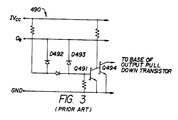
- a standard DC Miller killer circuit Figure 3
- Schottky transistor Q491 is held OFF by a LOW Oe through Schottky diode D492.
- Schottky transistor Q494 is ON, holding down the base of the output pulldown transistor and providing a low impedance path to ground for any charged coupled through its BC (Miller) capacitance.
- DC Miller killer circuit 450 by delaying its turn on and by limiting the discharge rate of the output pulldown transistor through circuit 450.
- the turn on of circuit 450 is delayed by the addition of pn diodes D456 and D457 (shown enhanced) between the collector of transistor Q454 and the base of transistor Q455, which increase the voltage swing required to turn on transistor Q455 and lowers the amount of base drive available to it.
- diodes D456 and D457 block discharge of stored charge in the base of Q455
- a discharge path is provided from the base of Q455 to ground through resistor R458 and diode D459 (shown enhanced).
- the discharge rate of the output pulldown transistor Q434 through circuit 450 is limited by the addition of resistor R460 (shown enhanced), having a low value of for example 500 ohms, in the collector circuit of transistor Q455.
- resistor R460 shown enhanced
- the value of resistor R460 should be limited to avoid negating the purpose of the DC Miller killer circuit 450.
Landscapes
- Engineering & Computer Science (AREA)
- Computer Hardware Design (AREA)
- Physics & Mathematics (AREA)
- Computing Systems (AREA)
- General Engineering & Computer Science (AREA)
- Mathematical Physics (AREA)
- Logic Circuits (AREA)
- Semiconductor Integrated Circuits (AREA)
- Lead Frames For Integrated Circuits (AREA)
Description
- This invention relates to reducing the effect of transients on integrated circuit operation, and more particularly to reducing on-chip power rail perturbations and the effect of power rail perturbations on the operation of high speed digital integrated circuits.
- Power rail perturbation is a transient condition found on the on-chip power distribution lines, most commonly Vcc and ground, of certain types of high speed digital integrated circuits. The condition arises during the switching of high current or high power circuits of the integrated circuit, due to the interaction of parasitic inductances with localized power surges. One type of power rail perturbation, ground bounce, occurs when the potential of the internal ground of the device changes relative to system ground. A related condition involving internal Vcc is known as Vcc squeeze. Ground bounce along, Vcc squeeze alone, or the combination of both cause spurious states and transitions to occur in the switched circuits as well as the other circuits coupled to the switched circuits, thereby corrupting retained data or causing spurious states or transitions to be transmitted in the output.
- From document EP-A-0 147 635 an integrated circuit output buffer is known, comprising an input circuit, an output circuit having an output pulldown transistor, and a DC Miller killer circuit. The DC Miller killer circuit owns a first transistor for discharging charge coupled through the Miller capacitance of said output pulldown transistor, a second transistor for switching said first transistor in response to an output enable signal, and a discharge path between the base of said first transistor and ground for discharging stored charge from the base of said first transistor.
- An object of the present invention is to reduce the effect of power rail perturbations on the performance of integrated output buffer circuits. The invention is defined by
claim 1. - The integrated circuit output buffer as claimed owns an input circuit, an output circuit with an output pulldown transistor, and a DC Miller killer circuit. The DC Miller killer is improved to avoid aggrevating ground bounce. The improvements include delaying the turn-on of the DC Miller killer circuit, and limiting the discharge rate of the output pulldown transistor through the DC Miller killer circuit.
- Figure 1
- illustrates a latch circuit modified to reduce power rail perturbations (not claimed).
- Figure 2
- illustrates an embodiment of the invention, and
- Figure 3
- is a schematic illustration of a standard DC Miller killer circuit.
- A schematic diagram of a
latch 300 and anoutput buffer 400, modified to reduce the effect of power rail perturbations, is set forth in Figures 1 and 2 respectively. Power is provided tolatch 300 and some circuits inbuffer 400 through isolated power rails 42 (IVcc) and 44 (IGND). Power is provided to other circuits inbuffer 400 through isolated power rails 52 (OVcc) and 54 (OGND). - Latch 300 is transparent to data applied to terminal 302 (DATA IN) when latch enable input signal Le is in a HIGH state. Latch enable signal Le is applied at
terminal 340, which is connected to the base of Schottky transistor Q311 inswitch 310 through Schottky diodes D341 and D342, and to the base of Schottky transistor Q324 in switch 30 through Schottky diode D343. Transistor Q324 is ON due to base drive through resistor 344, forward biasing the BE₂ junction of Schottky transistor Q321 inswitch 320 through the BC (shorted collector) diode D329. The potential at the base of transistor Q321 goes to about 2Vbe+Vce+Vsd above ground, which is not sufficient to turn transistor Q312 ON. Hence, so long as Le is HIGH, Q312 is unaffected by the level at DATA IN and remains OFF. - When DATA IN goes low, Schottky diode D313 conducts and pulls down the base of Schottky transistor Q311 in
switch 310, turning it OFF. Schottky transistor Q312 is OFF. Schottky transistor Q322 inswitch 320 turns OFF and allows Schottky transistor Q323 inswitch 320 to turn ON through resistor R325 and Schottky diode D328. As a result, (a) theoutput terminal 303 is brought LOW; and (b) the BE₁ junction of multiple emitter Schottky transistor Q321 is forward biased through resistor R326 and Schottky diode D327, whereby the potential at the base of transistor Q321 becomes Vbe+Vce+2Vsd above ground. Transistor Q312 remains OFF. - When DATA IN goes HIGH, transistor Q311 in
switch 310 conducts and turns transistor Q322 inswitch 320 ON. As a result, transistor Q323 inswitch 320 turns OFF, wherebyoutput terminal 303 is brought up to 3Vd through resistor R330, pn diodes D331 and D332, and BC (shorted collector) diode D333. - Data is latched by applying a LOW to Le terminal 340. The base of transistor Q311 is limited to 2Vsd+Vce by Schottky diodes 341 and 342 and the Vce of the latch enable buffer (not shown) to ensure that transistor Q311 is held OFF. At the same time, the base of transistor Q324 in
switch 320 is brought LOW through diode D343, and transistor Q324 turns OFF. As a result, the state of transistor Q323 prior to the HL transition of Le controls the state of transistor Q312 inswitch 310, which in turn maintains the state of transistor Q323. Assuming Q323 ON (logical LOW at DATA OUT), the potential at the base of Q321 is Vbe+2Vsd+Vce, which is not sufficient to turn ON transistors Q312 and Q322. Transistor Q323 remains ON. Assuming Q323 OFF (logical HIGH at DATA OUT), the potential at the base of Q321 rises from Vbe+2Vsd+Vce to 2Vbe+2Vsd as Le goes LOW, which is sufficient to keep transistors Q312 and Q322 ON. Transistor Q323 remains OFF. - As will be appreciated,
latch 300 is sensitive to power rail perturbations. Erroneous operation of thelatch 300 absent the power rail isolation feature occurs, for example, when thelatch 300 attempts to latch a LOW while the transceiver is recovering from negative ground bounce exceeding 2Vbe+Vsd(D328)-Vsd(D313) (less than about 1.5V). In this event, transistors Q311 and Q322 turn ON, and switch 320 latches a HIGH. Isolating the internal Vcc rail 42 andground rail 44 from the internaloutput power rails 52 and 54 (Figure 12B) does not allow output ground bounce of sufficient magnitude to couple intointernal IGND rail 44, thereby avoiding erroneous operation due to power rail perturbations. - An improved Schottky clamped
TTL output buffer 400 according to the present invention is shown in Figure 2. The circuit stages in thebuffer 400 preferably include theinput stage 410, aphase splitter stage 420, anoutput stage 430, asquaring network 480, an AC Miller killer circuit 440 (includingsections ground reference changer 470 may be provided to further reduce the effect of ground bounce; otherwise, the second emitter of transistor Q414 is omitted.Rail 42 is the isolated internal rail IVcc (see Figure 12A),rail 52 is the internal output OVcc rail, andrail 54 is the internal output ground OGND rail. - With Oe HIGH at
terminal 402, the operation of theoutput buffer 400 is as follows. Theinput stage 410 includes multiple emitter Schottky transistor Q414, the first emitter of which is connected to DATA IN throughterminal 401. When DATA IN is LOW, transistor Q414 is forward biased through resistor R412 and pulls its collector LOW. The LOW is applied to the common bases of Schottky transistors Q426 and Q427 inphase splitter 420. Transistors Q426 and Q427 do not cut in; as a result, the Darlington pair of Schottky transistor Q432 and transistor Q433 in theoutput stage 430 conducts through Schottky diode D431 and raises output terminal 403 HIGH. Note that thebuffer 400 is inverting. Pulldown transistor Q434 is OFF at this time. - When DATA IN goes high, transistor Q414 turns OFF and its BC junction becomes forward biased, which in turn forward biases transistors Q426 and Q427. Transistor Q427 pulls down the base of transistor Q432 in the Darlington pair, turning it and transistor Q433 OFF. About the same time, Transistor Q434 also becomes forward biased, its base flow obtained through resistor R428 and transistor Q427, resistor R423 and transistor Q426, and resistor R412 and the Schottky clamp of transistor Q414. Transistor Q434 pulls down output terminal 403, providing a LOW.
- Diodes D424 and D425 are speed up diodes to discharge capacitances. When transistor Q426 turns ON and its collector voltage falls, diode D424 provides a discharge path for internal capacitance at the base of transistor Q433. Diode D425 provides a discharge path for load capacitance at terminal 403 through transistor Q426 to increase the base current of transistor Q434 and improve its current sinking capability during the HIGH-to-LOW output voltage transition.
-
Squaring network 480 includes Schottky transistor Q481 and resistors R483 and R485, connected between the base of transistor Q434 and internaloutput ground rail 54. - The
output buffer 400 is tristated by application of a LOW to Oe terminal 402. In this event, the base of transistor Q414 in theinput stage 410 is pulled down through Schottky diode 406, the common base of transistors Q426 and Q427 in thephase splitter 420 is pulled down through Schottky diode D407, and the base of transistor Q432 in theoutput stage 430 is pulled down through Schottky diode D404. A high impedance is thus presented at the output terminal 403. - The dynamic
ground reference changer 470 functions to improve the noise margin at the interface of thelatch 300 andbuffer 400, which otherwise would be degraded by isolation of the respective internal power rails 42 and 44 from internal output power rails 52 and 54. - In the absence of
circuit 470, the LH transition on output terminal 403 will experience noise in the form of a flat spot, glitch, or oscillation, as follows. Assuming that transistor Q434 in theoutput stage 430 is loaded with current from a following device (not shown), a HL transition at thelatch input terminal 302 will cause transistor Q323 inlatch switch 320 to conduct. After some propagation delay time, transistor Q434 will turn OFF, causing a large negative di/dt along theoutput ground rail 54. Note that transistors Q426 and Q427 in thephase splitter 420 and transistor Q434 in theoutput stage 430 are held OFF by the path through Q414 ininput stage 410, and Q323 and diode D328 inswitch 320. When
then the LH transition on the collector of transistor Q434 will have a flat spot, glitch, or oscillation. - The dynamic
ground reference changer 470 functions to reference a second emitter of Q414 to outputinternal ground rail 54 instead of the isolatedinternal ground rail 44 during ground bounce. During an output LH transition at terminal 403, the cathode of diode D471 (shown enhanced), which is connected to the emitter of transistor Q432 in theoutput stage 430, begins to rise. Diode D471 is reversed biased, and couples sufficient current through its junction capacitance to the base of Schottky transistor Q474 (shown enhanced) to saturate it. Once saturated, transistor Q474 holds LOW the second emitter of transistor Q414, whereby the common base of transistors Q426 and Q427 inphase splitter 420 are referenced to output ground. During an output LH transition on other terminals of the octal registered transceiver when terminal 403 is high, the potential at the cathode of diode D471 falls slightly due to the di/dt of the charging current flowing in the Vcc power rails. Nonetheless, an occurrence of ground bounce will cause the anode of diode D471 to fall faster the falling potential at its cathode. Diode D471 is reversed biased, and again couples sufficient current to the base of transistor Q474 to saturate it. A suitable value for the junction capacitance of diode D471 is about 300 fF, bearing in mind that the actual value depends on the values selected by the designer for the other circuit components. Other elements incircuit 470 include diodes D472 and D473. Diode D472 is connected between the base of transistor Q474 and the base of pulldown transistor Q434 to avoid completely discharging the base of transistor Q474 when a falling transition is present at the N-side of diode D471. Diode D473 is connected between the collector of transistor Q474 and the second emitter of transistor Q414, for providing the same LOW level as provided by thelatch 300. - The AC Miller killer circuit 440 functions to improve the output rise time and minimize power consumption during repetitive switching. In principle, the AC Miller killer circuit 440 provides a momentary low impedance at the base of transistor Q434 during an output LH transition, thereby absorbing displacement current flowing through the collector-base capacitance of transistor Q434. In operation, rising voltage at the emitter of transistor Q432 causes displacement current to flow through BC diode D444, momentarily turning on transistor Q447. Transistor Q447 pulls down the base of transistor Q434 of the
output stage 430 to absorb the displacement current flowing through the CB capacitance of Q434. When Q434 turns ON, diode D444 is discharged by D424. Diode D446 optimizes the pulldown level of transistor 447. - Unfortunately, a standard AC Miller killer circuit aggravates power rail perturbation during an LZ transition at high speed and with heavy loads at the output. In a standard AC Miller killer circuit arrangement, the cathode of D444 would reference to the output (terminal 403) through only a resistor (not shown). While the output is relatively stable during an LZ transition, a power rail perturbation such as, for example, ground bounce, causes internal ground to fall, thereby increasing the voltage across diode D444. Diode D444 discharges into transistor Q447, turning it ON and draining off some base charge from Q434. As a result, the discharge rate of Q434 is hastened, aggravating the ground bounce.
- This problem is solved in AC Miller killer circuit 440 by removing the discharge effect. Schottky diode D405 (shown enhanced) functions to prevent circuit 440 from responding during an LZ transition by pulling the cathode of diode D444 to a level Vsd above Oe, thereby preventing the development of a positive dv/dt across diode D444 during ground bounce. Schottky diode D443 (shown enhanced) is added to the circuit referencing D444 to the output 403, so that Oe terminal 402 will not sink current through resistor 442 and diode D405 when output terminal 403 is tristated and the bus is brought HIGH.
- The DC Miller killer 450 provides the
output stage 430 with immunity from noise on the bus whenoutput buffer 400 is in tristate. A large positive voltage spike on the bus could couple charge across the Miller capacitance of transistor Q434 and erroneously turn it ON. In a standard DC Miller killer circuit (Figure 3), Schottky transistor Q491 is held OFF by a LOW Oe through Schottky diode D492. Schottky transistor Q494 is ON, holding down the base of the output pulldown transistor and providing a low impedance path to ground for any charged coupled through its BC (Miller) capacitance. - Unfortunately, a standard DC Miller killer circuit also aggravates power rail perturbation during an LZ transition at high speed and with heavy loads at the output. As Oe is brought LOW, Q494 rapidly turns ON and rapidly discharges the base of the output pulldown transistor, thereby aggravating ground bounce.
- This problem is solved in DC Miller killer circuit 450 by delaying its turn on and by limiting the discharge rate of the output pulldown transistor through circuit 450. The turn on of circuit 450 is delayed by the addition of pn diodes D456 and D457 (shown enhanced) between the collector of transistor Q454 and the base of transistor Q455, which increase the voltage swing required to turn on transistor Q455 and lowers the amount of base drive available to it. As diodes D456 and D457 block discharge of stored charge in the base of Q455, a discharge path is provided from the base of Q455 to ground through resistor R458 and diode D459 (shown enhanced). The discharge rate of the output pulldown transistor Q434 through circuit 450 is limited by the addition of resistor R460 (shown enhanced), having a low value of for example 500 ohms, in the collector circuit of transistor Q455. The value of resistor R460 should be limited to avoid negating the purpose of the DC Miller killer circuit 450.
Claims (2)
- An integrated circuit output buffer having an input circuit, and output circuit having an output pulldown transistor (Q434), and a DC Miller killer circuit, said DC Miller killer circuit comprising:
a first transistor (Q455) for discharging charge coupled through the Miller capacitance of said output pulldown transistor (Q434);
a first resistor (R485) connected between the collector of said first transistor (Q455) and the base of said output pulldown transistor (Q434), the value of said first resistor (R485) being selected to limit the discharge rate of said output pulldown transistor (Q434);
a second transistor (Q454) for switching said first transistor (Q455) in response to an output enable signal;
at least one diode (D456, D457) connected between the collector of said second transistor (Q454) and the base of said first transistor (Q455),
the number of diodes being selected to delay the turn-on of said first transistor (Q455); and
a discharge path including a resistor (R458) and a diode (D459) connected in series between the base of said first transistor (Q455) and ground, for discharging stored charge from the base of said first transistor (Q455). - An output buffer as in claim 1, wherein a Vcc power rail coupled to said input circuit and said DC Miller killer circuit is isolated from a Vcc power rail coupled to said output circuit.
Applications Claiming Priority (3)
| Application Number | Priority Date | Filing Date | Title |
|---|---|---|---|
| US88040786A | 1986-06-30 | 1986-06-30 | |
| US880407 | 1986-10-21 | ||
| EP87401418A EP0251880A3 (en) | 1986-06-30 | 1987-06-23 | Reduction in power rail perturbation and in the effect thereof on integrated circuit performance |
Related Parent Applications (2)
| Application Number | Title | Priority Date | Filing Date |
|---|---|---|---|
| EP87401418A Division EP0251880A3 (en) | 1986-06-30 | 1987-06-23 | Reduction in power rail perturbation and in the effect thereof on integrated circuit performance |
| EP87401418.6 Division | 1987-06-23 |
Publications (3)
| Publication Number | Publication Date |
|---|---|
| EP0448135A2 EP0448135A2 (en) | 1991-09-25 |
| EP0448135A3 EP0448135A3 (en) | 1992-03-25 |
| EP0448135B1 true EP0448135B1 (en) | 1995-11-08 |
Family
ID=25376209
Family Applications (2)
| Application Number | Title | Priority Date | Filing Date |
|---|---|---|---|
| EP91108783A Expired - Lifetime EP0448135B1 (en) | 1986-06-30 | 1987-06-23 | An output buffer circuit |
| EP87401418A Ceased EP0251880A3 (en) | 1986-06-30 | 1987-06-23 | Reduction in power rail perturbation and in the effect thereof on integrated circuit performance |
Family Applications After (1)
| Application Number | Title | Priority Date | Filing Date |
|---|---|---|---|
| EP87401418A Ceased EP0251880A3 (en) | 1986-06-30 | 1987-06-23 | Reduction in power rail perturbation and in the effect thereof on integrated circuit performance |
Country Status (5)
| Country | Link |
|---|---|
| EP (2) | EP0448135B1 (en) |
| JP (1) | JPS6326116A (en) |
| KR (1) | KR960013630B1 (en) |
| CA (1) | CA1320994C (en) |
| DE (1) | DE3751591T2 (en) |
Cited By (1)
| Publication number | Priority date | Publication date | Assignee | Title |
|---|---|---|---|---|
| US10897229B1 (en) | 2019-11-19 | 2021-01-19 | Seeya Optronics Co., Ltd. | Compensation circuit for operational amplifier, integrated circuit and display panel |
Families Citing this family (8)
| Publication number | Priority date | Publication date | Assignee | Title |
|---|---|---|---|---|
| JPS63234623A (en) * | 1987-03-23 | 1988-09-29 | Toshiba Corp | Semiconductor integrated circuit |
| EP0343633A3 (en) * | 1988-05-24 | 1991-03-06 | Kabushiki Kaisha Toshiba | Semiconductor integrated circuit |
| US5162894A (en) * | 1988-05-24 | 1992-11-10 | Kabushiki Kaisha Toshiba | Semiconductor integrated circuit having a dummy lead and shaped inner leads |
| US5089721A (en) * | 1990-04-20 | 1992-02-18 | National Semiconductor Corp. | Ground bounce isolation and high speed output circuit |
| US5204554A (en) * | 1991-12-06 | 1993-04-20 | National Semiconductor Corporation | Partial isolation of power rails for output buffer circuits |
| US5438277A (en) * | 1993-03-19 | 1995-08-01 | Advanced Micro Devices, Inc. | Ground bounce isolated output buffer |
| DE69418037T2 (en) * | 1994-08-02 | 1999-08-26 | Consorzio Per La Ricerca Sulla Microelettronica Ne | Power semiconductor device made of MOS technology chips and housing structure |
| US6246107B1 (en) * | 1999-07-07 | 2001-06-12 | Philips Semiconductors, Inc. | Semiconductor device arrangement having configuration via adjacent bond pad coding |
Family Cites Families (7)
| Publication number | Priority date | Publication date | Assignee | Title |
|---|---|---|---|---|
| US4339676A (en) * | 1979-08-13 | 1982-07-13 | Texas Instruments Incorporated | Logic circuit having a selectable output mode |
| GB2073947B (en) * | 1980-04-11 | 1983-12-21 | Philips Electronic Associated | Integrated circuit encapsulation |
| US4454529A (en) * | 1981-01-12 | 1984-06-12 | Avx Corporation | Integrated circuit device having internal dampening for a plurality of power supplies |
| US4572970A (en) * | 1982-11-19 | 1986-02-25 | Motorola, Inc. | Miller capacitance effect eliminator for use with a push-pull amplifier output stage |
| US4585959A (en) * | 1983-12-29 | 1986-04-29 | Motorola, Inc. | Tri-state logic gate having reduced Miller capacitance |
| JPS59215567A (en) * | 1984-02-08 | 1984-12-05 | 株式会社日立製作所 | Evaporator for refrigerator |
| WO1986005322A1 (en) * | 1985-02-28 | 1986-09-12 | Sony Corporation | Semiconducteur circuit device |
-
1987
- 1987-06-04 KR KR1019870005653A patent/KR960013630B1/en not_active Expired - Fee Related
- 1987-06-23 EP EP91108783A patent/EP0448135B1/en not_active Expired - Lifetime
- 1987-06-23 DE DE3751591T patent/DE3751591T2/en not_active Expired - Fee Related
- 1987-06-23 EP EP87401418A patent/EP0251880A3/en not_active Ceased
- 1987-06-29 CA CA000540803A patent/CA1320994C/en not_active Expired - Fee Related
- 1987-06-30 JP JP62161426A patent/JPS6326116A/en active Pending
Cited By (1)
| Publication number | Priority date | Publication date | Assignee | Title |
|---|---|---|---|---|
| US10897229B1 (en) | 2019-11-19 | 2021-01-19 | Seeya Optronics Co., Ltd. | Compensation circuit for operational amplifier, integrated circuit and display panel |
Also Published As
| Publication number | Publication date |
|---|---|
| DE3751591T2 (en) | 1996-06-05 |
| EP0448135A2 (en) | 1991-09-25 |
| EP0251880A3 (en) | 1988-08-03 |
| EP0251880A2 (en) | 1988-01-07 |
| JPS6326116A (en) | 1988-02-03 |
| KR880005677A (en) | 1988-06-30 |
| EP0448135A3 (en) | 1992-03-25 |
| KR960013630B1 (en) | 1996-10-10 |
| CA1320994C (en) | 1993-08-03 |
| DE3751591D1 (en) | 1995-12-14 |
Similar Documents
| Publication | Publication Date | Title |
|---|---|---|
| US5065224A (en) | Low noise integrated circuit and leadframe | |
| US5293081A (en) | Driver circuit for output buffers | |
| JPH06163824A (en) | Semiconductor integrated circuit | |
| US6400204B1 (en) | Input stage ESD protection for an integrated circuit | |
| JPH0783252B2 (en) | Semiconductor integrated circuit device | |
| US4508981A (en) | Driver circuitry for reducing on-chip Delta-I noise | |
| EP0448135A2 (en) | An output buffer circuit | |
| US5173621A (en) | Transceiver with isolated power rails for ground bounce reduction | |
| US5036215A (en) | Pass gate multiplexer receiver circuit | |
| JP2941579B2 (en) | Square law clamp circuit | |
| EP0622903A2 (en) | Input buffer circuit having sleep mode and bus hold function | |
| US4430585A (en) | Tristate transistor logic circuit with reduced power dissipation | |
| EP0305482B1 (en) | Low-noise transmission line termination circuitry | |
| US4851715A (en) | Schottky-clamped transistor logic buffer circuit | |
| US5296760A (en) | Voltage translator | |
| EP0452747A2 (en) | Ground bounce isolation network | |
| EP0032043B1 (en) | Transistor-transistor logic circuit | |
| EP0097788A2 (en) | Large swing driver/receiver circuit | |
| EP0155305B1 (en) | Emitter collector coupled logic | |
| JPH0720059B2 (en) | Transistor circuit | |
| JPS63115420A (en) | Bipolar logic circuit | |
| US4634898A (en) | TTL buffer circuit incorporating active pull-down transistor | |
| EP0054408B1 (en) | Logic circuit | |
| US5212617A (en) | Circuit for compensating very fast current fluctuations | |
| JP3164689B2 (en) | Tri-state buffer circuit |
Legal Events
| Date | Code | Title | Description |
|---|---|---|---|
| PUAI | Public reference made under article 153(3) epc to a published international application that has entered the european phase |
Free format text: ORIGINAL CODE: 0009012 |
|
| AC | Divisional application: reference to earlier application |
Ref document number: 251880 Country of ref document: EP |
|
| AK | Designated contracting states |
Kind code of ref document: A2 Designated state(s): DE FR GB IT NL |
|
| RIN1 | Information on inventor provided before grant (corrected) |
Inventor name: FRASER, DANA Inventor name: MATHIEU, GAETAN L. Inventor name: HANNINGTON, GEOFF Inventor name: MENTZER, RAY Inventor name: KEOWN, SUSAN Inventor name: GRAY, JERRY |
|
| PUAL | Search report despatched |
Free format text: ORIGINAL CODE: 0009013 |
|
| AK | Designated contracting states |
Kind code of ref document: A3 Designated state(s): DE FR GB IT NL |
|
| 17P | Request for examination filed |
Effective date: 19920714 |
|
| 17Q | First examination report despatched |
Effective date: 19950217 |
|
| GRAA | (expected) grant |
Free format text: ORIGINAL CODE: 0009210 |
|
| AC | Divisional application: reference to earlier application |
Ref document number: 251880 Country of ref document: EP |
|
| AK | Designated contracting states |
Kind code of ref document: B1 Designated state(s): DE FR GB IT NL |
|
| PG25 | Lapsed in a contracting state [announced via postgrant information from national office to epo] |
Ref country code: IT Free format text: LAPSE BECAUSE OF FAILURE TO SUBMIT A TRANSLATION OF THE DESCRIPTION OR TO PAY THE FEE WITHIN THE PRE;WARNING: LAPSES OF ITALIAN PATENTS WITH EFFECTIVE DATE BEFORE 2007 MAY HAVE OCCURRED AT ANY TIME BEFORE 2007. THE CORRECT EFFECTIVE DATE MAY BE DIFFERENT FROM THE ONE RECORDED.SCRIBED TIME-LIMIT Effective date: 19951108 Ref country code: FR Effective date: 19951108 Ref country code: NL Free format text: LAPSE BECAUSE OF FAILURE TO SUBMIT A TRANSLATION OF THE DESCRIPTION OR TO PAY THE FEE WITHIN THE PRESCRIBED TIME-LIMIT Effective date: 19951108 |
|
| REF | Corresponds to: |
Ref document number: 3751591 Country of ref document: DE Date of ref document: 19951214 |
|
| NLV1 | Nl: lapsed or annulled due to failure to fulfill the requirements of art. 29p and 29m of the patents act | ||
| EN | Fr: translation not filed | ||
| PG25 | Lapsed in a contracting state [announced via postgrant information from national office to epo] |
Ref country code: GB Effective date: 19960623 |
|
| PLBE | No opposition filed within time limit |
Free format text: ORIGINAL CODE: 0009261 |
|
| STAA | Information on the status of an ep patent application or granted ep patent |
Free format text: STATUS: NO OPPOSITION FILED WITHIN TIME LIMIT |
|
| 26N | No opposition filed | ||
| GBPC | Gb: european patent ceased through non-payment of renewal fee |
Effective date: 19960623 |
|
| PG25 | Lapsed in a contracting state [announced via postgrant information from national office to epo] |
Ref country code: DE Effective date: 19970301 |