EP0446927A1 - Dispositif photoélectrique supraconducteur fonctionnel - Google Patents
Dispositif photoélectrique supraconducteur fonctionnel Download PDFInfo
- Publication number
- EP0446927A1 EP0446927A1 EP91103959A EP91103959A EP0446927A1 EP 0446927 A1 EP0446927 A1 EP 0446927A1 EP 91103959 A EP91103959 A EP 91103959A EP 91103959 A EP91103959 A EP 91103959A EP 0446927 A1 EP0446927 A1 EP 0446927A1
- Authority
- EP
- European Patent Office
- Prior art keywords
- superconductive
- photo
- functional
- photoelectric device
- conductive
- Prior art date
- Legal status (The legal status is an assumption and is not a legal conclusion. Google has not performed a legal analysis and makes no representation as to the accuracy of the status listed.)
- Granted
Links
- 239000004065 semiconductor Substances 0.000 claims abstract description 42
- 239000010409 thin film Substances 0.000 claims abstract description 29
- 150000001875 compounds Chemical class 0.000 claims abstract description 22
- 230000004044 response Effects 0.000 claims abstract description 10
- 150000004770 chalcogenides Chemical class 0.000 claims abstract description 6
- 229910052714 tellurium Inorganic materials 0.000 claims description 7
- JBRZTFJDHDCESZ-UHFFFAOYSA-N AsGa Chemical compound [As]#[Ga] JBRZTFJDHDCESZ-UHFFFAOYSA-N 0.000 claims description 6
- 229910052738 indium Inorganic materials 0.000 claims description 6
- APFVFJFRJDLVQX-UHFFFAOYSA-N indium atom Chemical compound [In] APFVFJFRJDLVQX-UHFFFAOYSA-N 0.000 claims description 5
- 239000012535 impurity Substances 0.000 claims description 3
- RPPBZEBXAAZZJH-UHFFFAOYSA-N cadmium telluride Chemical compound [Te]=[Cd] RPPBZEBXAAZZJH-UHFFFAOYSA-N 0.000 claims 2
- 230000001678 irradiating effect Effects 0.000 claims 2
- 239000000463 material Substances 0.000 abstract description 11
- 230000000694 effects Effects 0.000 abstract description 5
- 238000001556 precipitation Methods 0.000 abstract description 4
- 239000004020 conductor Substances 0.000 abstract description 3
- 239000010408 film Substances 0.000 description 6
- 230000006870 function Effects 0.000 description 5
- 238000000034 method Methods 0.000 description 5
- 239000000758 substrate Substances 0.000 description 5
- 230000007704 transition Effects 0.000 description 5
- 229910001218 Gallium arsenide Inorganic materials 0.000 description 4
- 229910020658 PbSn Inorganic materials 0.000 description 3
- 101150071746 Pbsn gene Proteins 0.000 description 3
- OYLGJCQECKOTOL-UHFFFAOYSA-L barium fluoride Chemical compound [F-].[F-].[Ba+2] OYLGJCQECKOTOL-UHFFFAOYSA-L 0.000 description 3
- 229910001632 barium fluoride Inorganic materials 0.000 description 3
- 239000000969 carrier Substances 0.000 description 2
- 238000001514 detection method Methods 0.000 description 2
- 239000010931 gold Substances 0.000 description 2
- CPLXHLVBOLITMK-UHFFFAOYSA-N magnesium oxide Inorganic materials [Mg]=O CPLXHLVBOLITMK-UHFFFAOYSA-N 0.000 description 2
- 239000000395 magnesium oxide Substances 0.000 description 2
- AXZKOIWUVFPNLO-UHFFFAOYSA-N magnesium;oxygen(2-) Chemical compound [O-2].[Mg+2] AXZKOIWUVFPNLO-UHFFFAOYSA-N 0.000 description 2
- 238000012986 modification Methods 0.000 description 2
- 230000004048 modification Effects 0.000 description 2
- 230000002085 persistent effect Effects 0.000 description 2
- VYZAMTAEIAYCRO-UHFFFAOYSA-N Chromium Chemical compound [Cr] VYZAMTAEIAYCRO-UHFFFAOYSA-N 0.000 description 1
- GPXJNWSHGFTCBW-UHFFFAOYSA-N Indium phosphide Chemical compound [In]#P GPXJNWSHGFTCBW-UHFFFAOYSA-N 0.000 description 1
- XEEYBQQBJWHFJM-UHFFFAOYSA-N Iron Chemical compound [Fe] XEEYBQQBJWHFJM-UHFFFAOYSA-N 0.000 description 1
- 229910000661 Mercury cadmium telluride Inorganic materials 0.000 description 1
- XUIMIQQOPSSXEZ-UHFFFAOYSA-N Silicon Chemical compound [Si] XUIMIQQOPSSXEZ-UHFFFAOYSA-N 0.000 description 1
- ATJFFYVFTNAWJD-UHFFFAOYSA-N Tin Chemical compound [Sn] ATJFFYVFTNAWJD-UHFFFAOYSA-N 0.000 description 1
- QNBJSSZGYCOENO-UHFFFAOYSA-N [Cu].[Sr].[Ce].[Nd] Chemical compound [Cu].[Sr].[Ce].[Nd] QNBJSSZGYCOENO-UHFFFAOYSA-N 0.000 description 1
- 230000004888 barrier function Effects 0.000 description 1
- 230000005540 biological transmission Effects 0.000 description 1
- CJOBVZJTOIVNNF-UHFFFAOYSA-N cadmium sulfide Chemical compound [Cd]=S CJOBVZJTOIVNNF-UHFFFAOYSA-N 0.000 description 1
- 238000005229 chemical vapour deposition Methods 0.000 description 1
- 238000001816 cooling Methods 0.000 description 1
- 238000010586 diagram Methods 0.000 description 1
- 230000005284 excitation Effects 0.000 description 1
- PCHJSUWPFVWCPO-UHFFFAOYSA-N gold Chemical compound [Au] PCHJSUWPFVWCPO-UHFFFAOYSA-N 0.000 description 1
- 229910052737 gold Inorganic materials 0.000 description 1
- 238000009413 insulation Methods 0.000 description 1
- 150000002500 ions Chemical class 0.000 description 1
- 229910052745 lead Inorganic materials 0.000 description 1
- 239000007791 liquid phase Substances 0.000 description 1
- 238000005259 measurement Methods 0.000 description 1
- 230000003446 memory effect Effects 0.000 description 1
- 230000006386 memory function Effects 0.000 description 1
- 239000002184 metal Substances 0.000 description 1
- 229910052751 metal Inorganic materials 0.000 description 1
- 238000001451 molecular beam epitaxy Methods 0.000 description 1
- 230000003287 optical effect Effects 0.000 description 1
- 239000013307 optical fiber Substances 0.000 description 1
- 230000001681 protective effect Effects 0.000 description 1
- 229910052711 selenium Inorganic materials 0.000 description 1
- 239000011669 selenium Substances 0.000 description 1
- 229910052710 silicon Inorganic materials 0.000 description 1
- 239000010703 silicon Substances 0.000 description 1
- 238000001228 spectrum Methods 0.000 description 1
- PORWMNRCUJJQNO-UHFFFAOYSA-N tellurium atom Chemical compound [Te] PORWMNRCUJJQNO-UHFFFAOYSA-N 0.000 description 1
- 238000001771 vacuum deposition Methods 0.000 description 1
Images


Classifications
-
- H—ELECTRICITY
- H10—SEMICONDUCTOR DEVICES; ELECTRIC SOLID-STATE DEVICES NOT OTHERWISE PROVIDED FOR
- H10N—ELECTRIC SOLID-STATE DEVICES NOT OTHERWISE PROVIDED FOR
- H10N60/00—Superconducting devices
- H10N60/80—Constructional details
- H10N60/84—Switching means for devices switchable between superconducting and normal states
-
- H—ELECTRICITY
- H01—ELECTRIC ELEMENTS
- H01L—SEMICONDUCTOR DEVICES NOT COVERED BY CLASS H10
- H01L31/00—Semiconductor devices sensitive to infrared radiation, light, electromagnetic radiation of shorter wavelength or corpuscular radiation and specially adapted either for the conversion of the energy of such radiation into electrical energy or for the control of electrical energy by such radiation; Processes or apparatus specially adapted for the manufacture or treatment thereof or of parts thereof; Details thereof
- H01L31/0248—Semiconductor devices sensitive to infrared radiation, light, electromagnetic radiation of shorter wavelength or corpuscular radiation and specially adapted either for the conversion of the energy of such radiation into electrical energy or for the control of electrical energy by such radiation; Processes or apparatus specially adapted for the manufacture or treatment thereof or of parts thereof; Details thereof characterised by their semiconductor bodies
- H01L31/0256—Semiconductor devices sensitive to infrared radiation, light, electromagnetic radiation of shorter wavelength or corpuscular radiation and specially adapted either for the conversion of the energy of such radiation into electrical energy or for the control of electrical energy by such radiation; Processes or apparatus specially adapted for the manufacture or treatment thereof or of parts thereof; Details thereof characterised by their semiconductor bodies characterised by the material
- H01L31/0264—Inorganic materials
- H01L31/0296—Inorganic materials including, apart from doping material or other impurities, only AIIBVI compounds, e.g. CdS, ZnS, HgCdTe
- H01L31/02966—Inorganic materials including, apart from doping material or other impurities, only AIIBVI compounds, e.g. CdS, ZnS, HgCdTe including ternary compounds, e.g. HgCdTe
-
- H—ELECTRICITY
- H01—ELECTRIC ELEMENTS
- H01L—SEMICONDUCTOR DEVICES NOT COVERED BY CLASS H10
- H01L31/00—Semiconductor devices sensitive to infrared radiation, light, electromagnetic radiation of shorter wavelength or corpuscular radiation and specially adapted either for the conversion of the energy of such radiation into electrical energy or for the control of electrical energy by such radiation; Processes or apparatus specially adapted for the manufacture or treatment thereof or of parts thereof; Details thereof
- H01L31/0248—Semiconductor devices sensitive to infrared radiation, light, electromagnetic radiation of shorter wavelength or corpuscular radiation and specially adapted either for the conversion of the energy of such radiation into electrical energy or for the control of electrical energy by such radiation; Processes or apparatus specially adapted for the manufacture or treatment thereof or of parts thereof; Details thereof characterised by their semiconductor bodies
- H01L31/0256—Semiconductor devices sensitive to infrared radiation, light, electromagnetic radiation of shorter wavelength or corpuscular radiation and specially adapted either for the conversion of the energy of such radiation into electrical energy or for the control of electrical energy by such radiation; Processes or apparatus specially adapted for the manufacture or treatment thereof or of parts thereof; Details thereof characterised by their semiconductor bodies characterised by the material
- H01L31/0264—Inorganic materials
- H01L31/0304—Inorganic materials including, apart from doping materials or other impurities, only AIIIBV compounds
- H01L31/03046—Inorganic materials including, apart from doping materials or other impurities, only AIIIBV compounds including ternary or quaternary compounds, e.g. GaAlAs, InGaAs, InGaAsP
-
- H—ELECTRICITY
- H10—SEMICONDUCTOR DEVICES; ELECTRIC SOLID-STATE DEVICES NOT OTHERWISE PROVIDED FOR
- H10N—ELECTRIC SOLID-STATE DEVICES NOT OTHERWISE PROVIDED FOR
- H10N60/00—Superconducting devices
- H10N60/10—Junction-based devices
- H10N60/12—Josephson-effect devices
-
- H—ELECTRICITY
- H10—SEMICONDUCTOR DEVICES; ELECTRIC SOLID-STATE DEVICES NOT OTHERWISE PROVIDED FOR
- H10N—ELECTRIC SOLID-STATE DEVICES NOT OTHERWISE PROVIDED FOR
- H10N60/00—Superconducting devices
- H10N60/30—Devices switchable between superconducting and normal states
-
- Y—GENERAL TAGGING OF NEW TECHNOLOGICAL DEVELOPMENTS; GENERAL TAGGING OF CROSS-SECTIONAL TECHNOLOGIES SPANNING OVER SEVERAL SECTIONS OF THE IPC; TECHNICAL SUBJECTS COVERED BY FORMER USPC CROSS-REFERENCE ART COLLECTIONS [XRACs] AND DIGESTS
- Y10—TECHNICAL SUBJECTS COVERED BY FORMER USPC
- Y10S—TECHNICAL SUBJECTS COVERED BY FORMER USPC CROSS-REFERENCE ART COLLECTIONS [XRACs] AND DIGESTS
- Y10S505/00—Superconductor technology: apparatus, material, process
- Y10S505/825—Apparatus per se, device per se, or process of making or operating same
- Y10S505/848—Radiant energy application
Definitions
- the present invention relates to a functional photoelectric device utilizing a superconducting transition temperature enhancement effect caused by a light irradiation thereto. More particularly, it relates to a superconducting photoelectric device which can be employed as a high speed light switch device, a photo detector or a light memory device.
- a functional superconductive photoelectric device is constituted mainly with a compound semiconductor comprising lead chalcogenide doped with lead or indium.
- a compound semiconductor comprising lead chalcogenide doped with lead or indium.
- the new functional superconductive photoelectric device constituted with a superconductive thin film having an photo-conductive effect located between two electrodes, and converting from a normally conducting state to a superconducting state in response to a light irradiation thereto, is characterized in that the superconductive thin film is formed of a compound semiconductor of lead chalcogenide doped with lead (Pb) and/or indium (In).
- the new functional superconductive photoelectric device constituted with an photo-conductive region in contact with plural superconductive regions, is characterized in that a gap, filled with the photo-conductive region, between the plural superconductive regions is shorter than 500 times of a coherence length of the superconductivity, wherein upon a light irradiation thereto at a predetermined temperature the coherence length of the superconductivity in the photo-conductive region is extended so as to generate a superconductive characteristics therein.
- the present invention is based on a principle that in a photo-conductive material filled in a gap between closely located superconductive regions, a light irradiation thereto causes coherence length of the superconductivity to extend so that the photo-conductive gap is bridged by the superconductive regions.
- grain of the lead doped in the compound semiconductor of PbSnTe functions as a superconductive material and the PbSnTe semiconductor functions as a photo-conductive material.
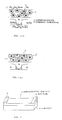
- Figs. 1(a) and (b) show a model of the above-described function principle.
- grains, i.e. precipitations, of the doped Pb are spatially distributing like stepping stones in a thin film 1 formed of Pb 1-x Sn x Te or Pb 1-x Sn x Te+In semiconductor.
- superconducting region of the Pb grains pass over Josephson junction between the Pb grain and Pb 1-x Sn x Te+In semiconductor, so as to penetrate into the semiconductor region 1 as indicated with shaded area 3.
- the coherence length of the superconductivity is not long enough to connect the Pb grains by the superconductive regions.
- photo carriers generated in the Pb 1-x Sn x Te /In semiconductor cause an extend of the coherence length of the superconductivity from each of the Pb grains. Consequently, the shaded areas indicating the superconducting state expand so as to be continuous with each other as shown in Fig. 1(b), so that the whole compound semiconductor thin film 1 becomes superconductive.
- the In grain forms a deep level so that the superconductivity is kept on even after the light irradiation is discontinued. Accordingly, thus provided persistent superconductivity allows to provide a photo memory device.
- Fig. 2 shows an example of a practical structure of the functional superconductive photoelectric device according to the present invention.
- a substrate 4 is formed of bariumfluoride (BaF2) measuring 1 mm x 5 mm, for example.
- Other materials such as magnesium oxide (MgO), semi-insulative gallium-arsenide (GaAs) or silicon (Si), can be employed for the substrate material, in place of the BaF2.
- a photo-conductive ternary semiconductor such as Pb 1-x Sn x Te, as a superconductive thin film 5 is deposited upon substrate 4 as thick as typically 1 ⁇ m by a hot wall method.
- electrodes 6a and 6b typically formed of gold (Au) or indium (In) are provided on both the ends of compound semiconductor thin film 5.
- a functional superconductive photoelectric device is fabricated.
- Other method such as vacuum deposition, liquid phase epitaxial grow method, molecular beam epitaxy (MBE) or metal organic chemical vapor deposition (MOCVD), may be employed for fabricating compound semiconductor thin film 5, in stead of the hot wall method.
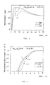
- the measure data is shown in Fig. 3, where the ordinate indicates the resistance value in ohm and the abscissa indicates the device temperature in degree K.
- Fig. 4 shows very low temperature part of Fig. 3 curves in an expanded scale in order to provide easier comprehension of the lower temperature characteristics, where the ordinate is normalized by the resistance value at 8 degree K.
- the solid line indicates dark state characteristic, when no light is irradiated thereto;
- the dotted line indicates the characteristics when an infrared light of wavelength spectrum having the peak at approximately 10 ⁇ m wave length is irradiated thereto from a 300 degrees K (i.e. room temperature) black body;
- the chain line indicates the characteristic when a 1 ⁇ m wavelength infrared light of 10 ⁇ W/cm2 strength is irradiated from a GaAs LED (light emitting diode) onto the photo-conductive thin film 5.
- the electrical resistance value of the above-described devices falls off at the temperature below 8 degrees K by an infrared light irradiation thereto, as well as the superconducting transition temperature T c shifts towards higher temperature, that is, the superconducting state is realized at a higher temperature.
- photo-conductive thin film 5 is in a normally conductive state in the dark state as indicated by curve 11 ; however, under an infrared light irradiation thereto from an LED, photo-conductive thin film 5 becomes superconductive having zero resistance value as indicated by curve 13, where it is observed that the resistance value shifts as much as range R off .
- At 3 degrees K under the infrared light irradiation it is observed that the resistance value falls off by a little over 50 % as shown by range R off' .
- each of precipitations of the doped impurities (Pb), or grains born from the precipitations forms a Josephson junction with the semiconductor material, where electrons in the semiconductor material are excited by the light irradiation thereto so as to rapidly increase the carrier concentration, which then causes the extend of the coherence length of the superconductivity from the Pb grains so that the coherence length reaches the same degree as the thickness of the barrier of the Josephson junction. Consequently, it is supposed that the whole semiconductor region becomes superconductive. Though it is observed that an approximately 2 % addition of Pb by weight is effective to enhance the superconducting transition temperature under the light irradiation, an addition of 1 to several percents of Pb also provides good results.
- the carrier concentration does not decrease, but keeping the superconducting state even after the light irradiation from the LED is discontinued. This is supposed to be owing to the contribution of the added In as an impurity. Accordingly, this compound semiconductor possessing a persistent photo-conductivity characteristic can be employed as a light memory device.
- Fig. 5 shows a basic circuit configuration employing the above-described functional photoelectrlc device as an optical switch.
- An electrode 6a at a one side of device 14 shown above in Fig. 2 is connected to a power source 15, and an electrode 6b at the other side as an output terminal is connected to a high impedance user's circuit 16.
- Functional photoelectric device 14 is mounted in a cooling dewer (not shown in the figure), shielded from light irradiation and kept at a predetermined temperature between 2 to 4 degrees K.
- An infrared light LED 17 is placed to face photo-conductive thin film 5, for inputting a signal light thereto. According to ON/OFF-switching of the LED, the resistance value of the photo-conductive thin film 5 varies so as to generate a high speed ON/OFF-switched signal in user's circuit 16.
- LED 17 may be replaced with an output end of an optical fiber transmission line connected to a distant signal source. More practically, a plurality of light switch devices 14 can be combined so as to constitute a light logic circuit common for the user,s circuit.
- FIG. 6 An input-ouput characteristics of light switch device 14 is shown in Figs. 6, where in response to the input signal (i.e. the ON/OFF of the signal light) shown in Fig. 6(a) from signal source 18 an output signal shown in Fig. 6 (b) appears at output terminal 66 of the device 14.
- an input light signal OFF-state photo-conductive thin film 5 being at a normally conducting state keeps the output signal at V n level; on the contrary, at an input light signal ON-state, photo-conductive thin film 5 being converted to a superconductive state makes the output terminal rapidly rise to a superconductive level V s which is close to the power source voltage. Therefore, a threshold level V th provided in advance in the user's circuit, between these two voltages, allows detection of the output signal component.
- the present invention utilizes a proximity effect caused from the light excitation of the superconductive grains (Pb or In) added in the photo-conductive semiconductor; therefore, the material having the photo-conductive effect is not limited only to the above-recited PbSnTe; but also other semi-insulative materials (having a low carrier concentration), in which high carrier mobility as well as long life time of the carrier are accomplished, can provide a similar functional photoelectric device based on the same principle.
- Compound semiconductors such as the above-recited Pb 1-x Sn x Te as well as other lead chalcogenides, such as PbCdTe (lead-cadnium-tellurium), PbSTe (lead-sulphor-tellurium) or PbSSe (lead-sulphor-selenium), possess a narrow band gap as well as a high carrier mobility, therefore, are suitable for a device which rapidly respond particularly to an infrared light.
- lead chalcogenides such as PbCdTe (lead-cadnium-tellurium), PbSTe (lead-sulphor-tellurium) or PbSSe (lead-sulphor-selenium
- a III-V group high resistance material in which the high resistivity is accomplished with GaAs doped with chrome (Cr), highly purified GaAs, or indium-phosphorus (InP) doped with iron (Fe) may be employed as the switching device by being added with the superconductive grains.
- a II-IV group compound semiconductor such as cadnium-tellurium (CdTe), mercury-cadnium-tellurium (HgCdTe) or cadmium-sulphur (CdS) may also alternatively employed thereto. Even in the above-cited case where GaAs or InP is employed, the persistently conductive photo-conductivity can be accomplished by introducing a DX center thereto.
- Fig. 7 shows a preferred embodiment of the case.
- a superconductive film 22 formed of, for example, neodymium-cerium-strontium-copper (NdCeSrCuO) is first deposited on a substrate 23. Next, a part of this film is removed to form a fine gap having a width d, by which two superconductive electrodes 22a and 22b are separated from each other.
- a photo-conductive thin film 21 formed of PbSnTe doped with In to accomplish a high resistance is deposited to fill at least the gap between two superconductive electrodes 22a and 22b, so as to fabricate a functional superconductive photo-electric device.
- the gap width d is particularly chosen to be below 500 times of the coherence length of the superconductivity, in consideration that the extended coherence length of the superconductivity becomes continuous with each other excited by the light irradiation.
- the coherence length of the superconductivity in a dark state is approximately 30 angstrom. Therefore, the gap width d is chosen to be 0.5 ⁇ m.
- Electrode terminals (not shown in the figure) are provided to both the super-conductive electrodes 22a and 22b, to which a constant current source is connected to measure the characteristics. The device of this configuration also exhibits the switching characteristic as well as the memory effect.
- the structure shown in Fig. 8 is also effective.
- a photo-conductive film 31 formed of compound semiconductor of lead chalcogenide is coated uniformly upon a substrate 33, over which the same superconductive film 32 as described above is then formed.
- a gap having the above-described width d is formed on a part of the superconductive film 32 so as to provide two superconductive electrodes 32a and 32b.
- a protective insulation film transparent to the input light may be further provided upon thus configurated device.
- a functional device operatable at a higher speed than the conventional switching devices and memory devices employing prior art electrical signals, are achieved. Therefore, a compact as well as high speed logic device can be accomplished by combining the functional superconductive photoelectric device of the present invention with a light IC (integrated circuit). Moreover, its light-responding feature allows an application in a light detection apparatus handling an infrared light.
- a device accomplishing a characteristic that a normally conducting state is switched to a superconductive stated in response to a light irradiation according to the present invention, allows to constitute various high speed logic circuits by being combined with a conventional device having a logically contrary characteristic that the superconductive state is converted to a normally conducting state in response to a light irradiation.
Landscapes
- Chemical & Material Sciences (AREA)
- Inorganic Chemistry (AREA)
- Physics & Mathematics (AREA)
- Condensed Matter Physics & Semiconductors (AREA)
- Electromagnetism (AREA)
- General Physics & Mathematics (AREA)
- Engineering & Computer Science (AREA)
- Computer Hardware Design (AREA)
- Microelectronics & Electronic Packaging (AREA)
- Power Engineering (AREA)
- Superconductor Devices And Manufacturing Methods Thereof (AREA)
- Light Receiving Elements (AREA)
- Inorganic Compounds Of Heavy Metals (AREA)
Applications Claiming Priority (3)
| Application Number | Priority Date | Filing Date | Title |
|---|---|---|---|
| JP2064551A JP2503091B2 (ja) | 1990-03-14 | 1990-03-14 | 超電導光機能素子 |
| JP6455190 | 1990-03-14 | ||
| JP64551/90 | 1990-03-14 |
Publications (2)
| Publication Number | Publication Date |
|---|---|
| EP0446927A1 true EP0446927A1 (fr) | 1991-09-18 |
| EP0446927B1 EP0446927B1 (fr) | 2002-07-03 |
Family
ID=13261473
Family Applications (1)
| Application Number | Title | Priority Date | Filing Date |
|---|---|---|---|
| EP91103959A Expired - Lifetime EP0446927B1 (fr) | 1990-03-14 | 1991-03-14 | Dispositif photoélectrique supraconducteur fonctionnel |
Country Status (5)
| Country | Link |
|---|---|
| US (1) | US5448098A (fr) |
| EP (1) | EP0446927B1 (fr) |
| JP (1) | JP2503091B2 (fr) |
| KR (1) | KR950000523B1 (fr) |
| DE (1) | DE69133052T2 (fr) |
Cited By (4)
| Publication number | Priority date | Publication date | Assignee | Title |
|---|---|---|---|---|
| DE19705239A1 (de) * | 1997-02-12 | 1998-08-20 | Georg Bastian | Optoelektronische Anordnung |
| US5955743A (en) * | 1995-03-01 | 1999-09-21 | Schroeder; Hehrwart | Superconductive tunnel elements, tunnel stacks produced therefrom and use thereof |
| EP1427028A1 (fr) * | 2001-09-14 | 2004-06-09 | National Institute of Advanced Industrial Science and Technology | Element de conversion ultra-rapide de signaux photoelectriques |
| WO2022152977A1 (fr) * | 2021-01-12 | 2022-07-21 | Buendia Jose | De la lumiere au centre de la matiere |
Families Citing this family (12)
| Publication number | Priority date | Publication date | Assignee | Title |
|---|---|---|---|---|
| US5768002A (en) * | 1996-05-06 | 1998-06-16 | Puzey; Kenneth A. | Light modulation system including a superconductive plate assembly for use in a data transmission scheme and method |
| US6015977A (en) * | 1997-01-28 | 2000-01-18 | Micron Technology, Inc. | Integrated circuit memory cell having a small active area and method of forming same |
| JP2955931B1 (ja) * | 1998-07-17 | 1999-10-04 | セイコーインスツルメンツ株式会社 | 放射線検出素子 |
| US6107643A (en) * | 1999-03-24 | 2000-08-22 | Abb Ab | Photoconductive switch with doping adapted to the intensity distribution of an illumination source thereof |
| JP2003101089A (ja) * | 2001-09-21 | 2003-04-04 | Central Japan Railway Co | 永久電流スイッチ材料及びその製造方法 |
| US6967344B2 (en) * | 2003-03-10 | 2005-11-22 | Energy Conversion Devices, Inc. | Multi-terminal chalcogenide switching devices |
| US20040201036A1 (en) * | 2003-04-08 | 2004-10-14 | Kiki Ikossi | Electronic device with barium fluoride substrate |
| US6990008B2 (en) * | 2003-11-26 | 2006-01-24 | International Business Machines Corporation | Switchable capacitance and nonvolatile memory device using the same |
| US7130212B2 (en) * | 2003-11-26 | 2006-10-31 | International Business Machines Corporation | Field effect device with a channel with a switchable conductivity |
| EP1943016B1 (fr) | 2005-10-14 | 2012-08-15 | Vive Crop Protection Inc. | Nanoparticules composites, nanoparticules et leurs procedes de fabrication |
| US8674302B2 (en) * | 2009-06-01 | 2014-03-18 | The United States Of America As Represented By The Administrator Of The National Aeronautics Space Administration | Superconducting transition edge sensors and methods for design and manufacture thereof |
| US11563162B2 (en) * | 2020-01-09 | 2023-01-24 | International Business Machines Corporation | Epitaxial Josephson junction transmon device |
Family Cites Families (6)
| Publication number | Priority date | Publication date | Assignee | Title |
|---|---|---|---|---|
| US4843446A (en) * | 1986-02-27 | 1989-06-27 | Hitachi, Ltd. | Superconducting photodetector |
| JPS63239877A (ja) * | 1987-03-26 | 1988-10-05 | Sumitomo Electric Ind Ltd | 超電導光トランジスタ |
| US5057485A (en) * | 1987-05-15 | 1991-10-15 | Hitachi, Ltd. | Light detecting superconducting Josephson device |
| US4837609A (en) * | 1987-09-09 | 1989-06-06 | American Telephone And Telegraph Company, At&T Bell Laboratories | Semiconductor devices having superconducting interconnects |
| US4990487A (en) * | 1988-03-11 | 1991-02-05 | The University Of Tokyo | Superconductive optoelectronic devices |
| US4970395A (en) * | 1988-12-23 | 1990-11-13 | Honeywell Inc. | Wavelength tunable infrared detector based upon super-schottky or superconductor-insulator-superconductor structures employing high transition temperature superconductors |
-
1990
- 1990-03-14 JP JP2064551A patent/JP2503091B2/ja not_active Expired - Lifetime
-
1991
- 1991-03-14 KR KR1019910004065A patent/KR950000523B1/ko not_active IP Right Cessation
- 1991-03-14 EP EP91103959A patent/EP0446927B1/fr not_active Expired - Lifetime
- 1991-03-14 DE DE69133052T patent/DE69133052T2/de not_active Expired - Fee Related
-
1992
- 1992-08-25 US US07/934,306 patent/US5448098A/en not_active Expired - Lifetime
Non-Patent Citations (7)
| Title |
|---|
| HITACHI REVIEW. vol. 39, no. 1, February 1990, TOKYO JP pages 35 - 40; T.Nishino et al.: "The field-effect superconducting transistor" * |
| JAPANESE JOURNAL OF APPLIED PHYSICS, SUPPLEMENTS. vol. 26-3, 1987, TOKYO JA pages 1345 - 1346; S.Takaoka et al.: "Superconductivity of (Pb,Sn,Ge)Te semiconductor film with a little Pb inclusion" * |
| PATENT ABSTRACTS OF JAPAN vol. 13, no. 44 (E-710) 31 January 1989, & JP-A-63 239877 (SUMITOMO) 05 October 1988, * |
| PHYSICAL REVIEW LETTERS. vol. 20, no. 23, 03 June 1968, NEW YORK US pages 1286 - 1289; I.Giaever: "Photosensitive tunneling and supercondictivity" * |
| PHYSICS LETTERS, A. vol. 71A, no. 5,6, 28 May 1979, AMSTERDAM NL pages 471 - 472; G.Deutscher et al.: "A granular photosuperconductor" * |
| SOLID STATE COMMUNICATIONS. vol. 76, no. 1, July 1990, OXFORD GB pages 31 - 34; T.Koshindo et al.: "Enhancement of superconducting transition temperature by photo-carriers in indium doped PbSnTe film with lead inclusion" * |
| SOVIET PHYSICS SEMICONDUCTORS. vol. 17, no. 12, December 1983, NEW YORK US pages 1396 - 1399; I.I.Zasavitskil et al.: "Kinetics of the photoconductivity of PbSnTe:In" * |
Cited By (5)
| Publication number | Priority date | Publication date | Assignee | Title |
|---|---|---|---|---|
| US5955743A (en) * | 1995-03-01 | 1999-09-21 | Schroeder; Hehrwart | Superconductive tunnel elements, tunnel stacks produced therefrom and use thereof |
| DE19705239A1 (de) * | 1997-02-12 | 1998-08-20 | Georg Bastian | Optoelektronische Anordnung |
| EP1427028A1 (fr) * | 2001-09-14 | 2004-06-09 | National Institute of Advanced Industrial Science and Technology | Element de conversion ultra-rapide de signaux photoelectriques |
| EP1427028A4 (fr) * | 2001-09-14 | 2009-08-12 | Nat Inst Of Advanced Ind Scien | Element de conversion ultra-rapide de signaux photoelectriques |
| WO2022152977A1 (fr) * | 2021-01-12 | 2022-07-21 | Buendia Jose | De la lumiere au centre de la matiere |
Also Published As
| Publication number | Publication date |
|---|---|
| US5448098A (en) | 1995-09-05 |
| DE69133052T2 (de) | 2003-02-06 |
| JP2503091B2 (ja) | 1996-06-05 |
| DE69133052D1 (de) | 2002-08-08 |
| JPH03265176A (ja) | 1991-11-26 |
| KR910017689A (ko) | 1991-11-05 |
| EP0446927B1 (fr) | 2002-07-03 |
| KR950000523B1 (ko) | 1995-01-24 |
Similar Documents
| Publication | Publication Date | Title |
|---|---|---|
| US5448098A (en) | Superconductive photoelectric switch | |
| US4679063A (en) | Infra red detectors | |
| US4236829A (en) | Solid-state image sensor | |
| US4970395A (en) | Wavelength tunable infrared detector based upon super-schottky or superconductor-insulator-superconductor structures employing high transition temperature superconductors | |
| EP0407166B1 (fr) | Appareil et procédé pour la détection de lumière | |
| US6111254A (en) | Infrared radiation detector | |
| JP2706029B2 (ja) | p−i−nダイオード | |
| US5494833A (en) | Backside illuminated MSM device method | |
| US5608255A (en) | FET optical receiver using backside illumination, indium materials species | |
| Gao et al. | In0. 53Ga0. 47As metal‐semiconductor‐metal photodiodes with transparent cadmium tin oxide Schottky contacts | |
| US3443166A (en) | Negative resistance light emitting solid state diode devices | |
| EP0063422B1 (fr) | Détecteur photoconducteur rapide à hétérojonction et à contact interdigité | |
| Kennedy et al. | High-performance 8—14-µm Pb 1-x Sn x Te photodiodes | |
| Frederikse et al. | Photoeffects in intermetallic compounds | |
| US4021833A (en) | Infrared photodiode | |
| Takasaki et al. | Avalanche multiplication of photo-generated carriers in amorphous semiconductor, and its application to imaging device | |
| EP0775371B1 (fr) | Composés et dispositifs infrarouges comportant un composé semiconducteur stoechiometrique d'indium et de thallium et comprenant au moins l'un des éléments arsenic et phosphore | |
| US3558920A (en) | Bistable photosensitive device utilizing tunnel currents in low resistive state | |
| EP0132326A2 (fr) | Passivation et isolation de dispositifs III-V | |
| US5231295A (en) | Superconducting field effect transistor | |
| US4696648A (en) | Heterostructure interdigital high speed photoconductive detector | |
| US5079610A (en) | Structure and method of fabricating a trapping-mode | |
| US4914495A (en) | Photodetector with player covered by N layer | |
| GB2206447A (en) | Lensed photodetector | |
| EP0271522A1 (fr) | Detecteur a bande de blocage d'impuretes a contact par l'arriere |
Legal Events
| Date | Code | Title | Description |
|---|---|---|---|
| PUAI | Public reference made under article 153(3) epc to a published international application that has entered the european phase |
Free format text: ORIGINAL CODE: 0009012 |
|
| AK | Designated contracting states |
Kind code of ref document: A1 Designated state(s): DE FR GB NL |
|
| 17P | Request for examination filed |
Effective date: 19920318 |
|
| 17Q | First examination report despatched |
Effective date: 19940601 |
|
| GRAG | Despatch of communication of intention to grant |
Free format text: ORIGINAL CODE: EPIDOS AGRA |
|
| GRAG | Despatch of communication of intention to grant |
Free format text: ORIGINAL CODE: EPIDOS AGRA |
|
| GRAH | Despatch of communication of intention to grant a patent |
Free format text: ORIGINAL CODE: EPIDOS IGRA |
|
| GRAH | Despatch of communication of intention to grant a patent |
Free format text: ORIGINAL CODE: EPIDOS IGRA |
|
| GRAA | (expected) grant |
Free format text: ORIGINAL CODE: 0009210 |
|
| AK | Designated contracting states |
Kind code of ref document: B1 Designated state(s): DE FR GB NL |
|
| REF | Corresponds to: |
Ref document number: 69133052 Country of ref document: DE Date of ref document: 20020808 |
|
| ET | Fr: translation filed | ||
| PLBE | No opposition filed within time limit |
Free format text: ORIGINAL CODE: 0009261 |
|
| STAA | Information on the status of an ep patent application or granted ep patent |
Free format text: STATUS: NO OPPOSITION FILED WITHIN TIME LIMIT |
|
| 26N | No opposition filed |
Effective date: 20030404 |
|
| PGFP | Annual fee paid to national office [announced via postgrant information from national office to epo] |
Ref country code: NL Payment date: 20080316 Year of fee payment: 18 Ref country code: GB Payment date: 20080312 Year of fee payment: 18 |
|
| PGFP | Annual fee paid to national office [announced via postgrant information from national office to epo] |
Ref country code: FR Payment date: 20080311 Year of fee payment: 18 Ref country code: DE Payment date: 20080306 Year of fee payment: 18 |
|
| GBPC | Gb: european patent ceased through non-payment of renewal fee |
Effective date: 20090314 |
|
| NLV4 | Nl: lapsed or anulled due to non-payment of the annual fee |
Effective date: 20091001 |
|
| REG | Reference to a national code |
Ref country code: FR Ref legal event code: ST Effective date: 20091130 |
|
| PG25 | Lapsed in a contracting state [announced via postgrant information from national office to epo] |
Ref country code: DE Free format text: LAPSE BECAUSE OF NON-PAYMENT OF DUE FEES Effective date: 20091001 |
|
| PG25 | Lapsed in a contracting state [announced via postgrant information from national office to epo] |
Ref country code: NL Free format text: LAPSE BECAUSE OF NON-PAYMENT OF DUE FEES Effective date: 20091001 |
|
| PG25 | Lapsed in a contracting state [announced via postgrant information from national office to epo] |
Ref country code: FR Free format text: LAPSE BECAUSE OF NON-PAYMENT OF DUE FEES Effective date: 20091123 Ref country code: GB Free format text: LAPSE BECAUSE OF NON-PAYMENT OF DUE FEES Effective date: 20090314 |