EP0446437A2 - Optical matrix - Google Patents
Optical matrix Download PDFInfo
- Publication number
- EP0446437A2 EP0446437A2 EP90123235A EP90123235A EP0446437A2 EP 0446437 A2 EP0446437 A2 EP 0446437A2 EP 90123235 A EP90123235 A EP 90123235A EP 90123235 A EP90123235 A EP 90123235A EP 0446437 A2 EP0446437 A2 EP 0446437A2
- Authority
- EP
- European Patent Office
- Prior art keywords
- optical
- matrix
- waveguides
- coupler
- matrix according
- Prior art date
- Legal status (The legal status is an assumption and is not a legal conclusion. Google has not performed a legal analysis and makes no representation as to the accuracy of the status listed.)
- Ceased
Links
Images

Classifications
-
- G—PHYSICS
- G02—OPTICS
- G02B—OPTICAL ELEMENTS, SYSTEMS OR APPARATUS
- G02B6/00—Light guides; Structural details of arrangements comprising light guides and other optical elements, e.g. couplings
- G02B6/24—Coupling light guides
- G02B6/26—Optical coupling means
- G02B6/35—Optical coupling means having switching means
- G02B6/351—Optical coupling means having switching means involving stationary waveguides with moving interposed optical elements
- G02B6/3534—Optical coupling means having switching means involving stationary waveguides with moving interposed optical elements the optical element being diffractive, i.e. a grating
-
- G—PHYSICS
- G02—OPTICS
- G02B—OPTICAL ELEMENTS, SYSTEMS OR APPARATUS
- G02B6/00—Light guides; Structural details of arrangements comprising light guides and other optical elements, e.g. couplings
- G02B6/24—Coupling light guides
- G02B6/26—Optical coupling means
- G02B6/35—Optical coupling means having switching means
- G02B6/354—Switching arrangements, i.e. number of input/output ports and interconnection types
- G02B6/3544—2D constellations, i.e. with switching elements and switched beams located in a plane
- G02B6/3546—NxM switch, i.e. a regular array of switches elements of matrix type constellation
-
- G—PHYSICS
- G02—OPTICS
- G02B—OPTICAL ELEMENTS, SYSTEMS OR APPARATUS
- G02B6/00—Light guides; Structural details of arrangements comprising light guides and other optical elements, e.g. couplings
- G02B6/24—Coupling light guides
- G02B6/26—Optical coupling means
- G02B6/35—Optical coupling means having switching means
- G02B6/3596—With planar waveguide arrangement, i.e. in a substrate, regardless if actuating mechanism is outside the substrate
Definitions
- the invention relates to an optical matrix according to the preamble of patent claim 1.
- Matrices of the type mentioned include, for example, switching matrices in which an optical coupler which can be switched individually between two switching states is arranged in each crossing point between a first and a second waveguide and which, in one of the two switching states, has a power component in one of the two at this crossing point crossing waveguide-guided optical wave in the other of these two waveguides.
- Couplers with a directional coupler structure are not suitable for large switching matrices because of their large overall length.
- Couplers with a crossover structure appear more suitable for large switching matrices.
- the main configurations of this structure are the y-fork (see Appl. Physics Letters 29, 1976, p. 790), the BOA structure (see Appl. Physics Letters 31, 1977, p. 266), the Bragg switch (see Appl. Physics Letters 33, 1978, p. 33), the x switch (see Electron. Letters 19, 1983, p. 553) and the switch with total internal reflection (see IEEE J. Quantum Electron. QE-14, 1978 , P. 513). Since the coupling areas in these couplers are multi-mode and the crossing angle is only a few degrees, the crosstalk is high, typically -20 dB, occasional best values are given as -30 dB. In addition, the insertion losses are high in the Bragg switch known from the above literature, as stated there, so that this switch type is unsuitable for a switching matrix for this reason alone.
- a further possibility of realizing an optical coupler for a switching matrix is to control the coupling out via an electro-optically generated homogeneous area of high refractive index.
- This possibility is out of the question because the effects are too small because the jumps in refractive index that can be achieved with these materials and the reflectivities that can be achieved with them are far too small. For example, achieved one in LiNbO3 a refractive index jump ⁇ n in the order of only 10 ⁇ 3.
- a large extension of the switching matrix is not only undesirable for technological reasons, but also when all optical couplers are to be electrically controlled synchronously by switching signals supplied from the outside, because the RC time constant of the electrical lines becomes problematic.
- the object of the invention is to provide a matrix of the type mentioned, which can be implemented in the smallest space with a large number of, for example, 100 ⁇ 100 or more optical couplers.
- the matrix according to the invention can have both one or more switchable couplers and one or more non-switchable couplers with a fixed degree of decoupling.
- a matrix with switchable couplers forms an optical switching matrix.
- each optical coupler is a non-switchable or non-switchable coupler with a fixed degree of coupling-out.
- the fixed degree of decoupling can essentially be chosen arbitrarily, in particular also greater than the low degree of decoupling of the switchable couplers.
- a switching matrix according to the invention can advantageously be used as a synapse matrix for an optically operating artificial neural network (claim 11), as a matrix in a distribution network (claim 12) and as an optical mixer (claim 13).
- first waveguide eW i and a second waveguide zW j are arranged with an optical coupler K ij which can be switched individually between two switching states.
- Each of these optical couplers K ij is designed in such a way that, in one of the two switching states, it couples a power component of an optical wave guided in one of the two waveguides eW i and zW j crossing at this crossing point into the other of these two waveguides eW i and zW j , it being essential that the degree of decoupling of this coupler K ij , ie the ratio between that decoupled from this coupler K ij
- the proportion of power to the power of the optical wave fed to this coupler K ij is deliberately low, and that the coupler K ij in the other switching state has an even smaller degree of decoupling than the low degree of decoupling.
- a low degree of decoupling means that this degree of decoupling is at least of the same order of magnitude or preferably less than the reciprocal 1 / M or 1 / N of the number M or N of the first or second waveguides eW i or zW j .
- the even smaller degree of decoupling should be as small as possible, ideally zero. It is also favorable if the transmission loss of the waveguides and couplers is as small as possible, ideally zero.
- the deliberately low degree of decoupling advantageously has the result that the first and second waveguides eW i and zW j can cross at a very large angle, in particular at an angle of 90 °, and that the couplers K ij are designed with an extremely short coupling or installation length can be made, which in turn enables matrices with an extremely large number of couplers and extremely small dimensions.
- the couplers with Mach-Zehnder structure or directional coupler structure are less good or not suitable.
- the actual coupling zone could be selected to be negligibly short in order to achieve the desired low degree of decoupling, but this would not significantly reduce the overall length of the coupler because the angle between the input waveguides leading to the coupling zone and the output waveguides continuing from this zone Avoidance of losses caused by waveguide curvatures is only about 1 °.
- couplers with cross-over or x structure are suitable for implementing couplers K ij with a low degree of decoupling and an extremely short overall length.
- Each coupler K ij of the matrix according to FIG. 1 allows, for example, an optical wave guided from left to right in the first waveguide eW i in question, but in the one switching state couples a low power component of this optical wave corresponding to the low degree of decoupling into the relevant second waveguide zW j in which this share of performance is continued, for example downwards.
- all couplers K ij in particular couple out in the same direction.
- each coupler has the vertical arrows pointing downward, an optical wave coming up from the right, an optical wave coming from below to the left and one from above coming optical wave partially coupled out to the right.
- the concentrator function is obtained because the power components decoupled by the couplers K ij into a second waveguide zW j of optical waves guided in the first waveguides eW i are fed to a single output A ' j of the matrix on this second waveguide zW j . In addition, these power components add up.
- this attenuation is at least approximately -30 dB when using electro-optical materials and at least approximately -20 dB when using organic materials for the couplers K ij .
- the transmission loss in a conventional matrix with M inputs and N outputs using conventional electro-optical couplers increases linearly with the number of crossing points of the matrix, ie the transmission loss in such matrices is approximately (M + N) dB.
- the crosstalk per crossing point of the matrix is less than -80 dB.
- crosstalk in conventional electro-optical switches cannot be significant due to the small angle of about 1 ° between the feeding and the continuing optical waveguides depending on the ratio between the transverse diameter and the width of the waveguide and the wavelength of -20 dB to -30 dB fall below.
- the first and second waveguides eW i and zW j consist of strip-like waveguides integrated on a common substrate made of electro-optical material, for example L i NbO3, which are in a common Are arranged plane and intersect at least substantially vertically at the crossing points.
- optical coupler K ij each consist of an electro-optically producible Bragg grating, the grating lines GL of which run at least substantially at an angle of 45 ° to the respective longitudinal direction R 1 and R 2 of the first and second waveguides eW i and zW j which are in the same direction R for all couplers K ij .
- the linear dimension of a 1000x1000 matrix is then less than 10 mm.
- the coupling length L of the optical couplers with the low degree of coupling-out is very short, for example 10 ⁇ m.
- a linear expansion of the matrix becomes extremely small at a distance between the crossing points of the order of magnitude of 10 ⁇ m, even with a large number of crossing points. It is about 10.N ⁇ m, in conventional matrices, however, at least 8.N mm.
- the connection network of the neurons plays a decisive role in such neural networks. The strength of this connection represents the information stored.
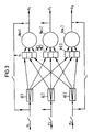
- Figure 3 the essential functional blocks of an exemplary and optically realizable neural network for three neurons Neu1, Neu2 and Neu3 are shown schematically.
- Input signals e1 to e3 are each divided in terms of performance in assigned signal splitting devices AE1 to AE3, the divided signals of different splitting devices AE1 to AE3 are multiplied in matrix multiplication devices ME1 to ME3 by matrix elements g ij and then added or integrated in a neuron Neu1, Neu2 and Neu3 and changed in accordance with the transfer function of the neuron.
- the system has formed an associated output pattern consisting of the input signals e 1, e 2, e 3 and an output pattern consisting of output signals a 1, a 2 and a 3.
- a device that performs such a matrix-vector multiplication with the required summation is referred to as a synapse matrix.
- the physical implementation of such a synapse matrix is of central importance for neural networks.
- the synapse matrix should also work optically, ie that the input signals e 1 to e M and output signals a 1 to a N forming a vector or a pattern are present optically and the input signals in the matrix are processed optically.
- the matrix according to the invention according to FIG. 1 or 2 can advantageously be used as an optically operating synapse matrix, since in this matrix the power components decoupled by the couplers K ij into the second waveguide zW j add up to form a sum signal. Because of the reciprocity of the optical couplers K ij , this sum signal is weakened in the relevant intersection points, but only slightly according to the number of these intersection points.
- a matrix according to the invention with M inputs and N outputs also realizes a complete neural network of the structure according to FIG. 3 with N neurons for M input signals e 1 to e M , because, due to the broadcasting function implemented on the first waveguides eW i , advantageously the signal splitting devices at the same time AEi are inherently realized.
- the degree of decoupling of each coupler K ij should be of the order of 1 / (10th N), which corresponds to a decoupling of -30 dB or an insertion loss of +30 dB for 100 outputs or neurons.
- the problem of control of the coupler K ij can be solved so that the control information of each coupler K ij assigned as the charge amount on a this coupler K ij capacitor C ij, is stored for example in the FET embodiment, which is practically unloaded via a high-impedance output and optionally feeds the electrodes of the coupler K ij .
- the matrices in distribution networks are also subject to demands for low insertion losses, low crosstalk and short overall lengths.
- Signals from any of the M inputs E i are to be switched through to any of the N outputs A j . It may be desirable that an input signal e i is switched to only one output A j or to several outputs simultaneously.
- the degree of decoupling is again selected 1 / (10.N).
- the insertion loss in the matrix according to the invention is approximately (10 + 10 log N) dB.
- the loss between input and output increases linearly with the number of crosspoints, so it is (M + N) dB.
- amplifiers with a non-linear characteristic curve could be provided on the first waveguides eW i which have the broadcasting function and raise the power levels to a constant value along these first waveguides eW i .
- Amplifiers for raising the signal level can be provided at the outputs A j of the matrix.
- the exemplary matrix according to FIG. 4 differs from the exemplary matrix according to FIG. 2 only in the couplers K ij , which in the matrix according to FIG. 4 are non-switchable couplers with a fixed degree of decoupling.
- the first and second optical waveguides eW i and zW j each have, for example, a triangular region Be with a refractive index n 1 that is higher than the refractive index n0 of the waveguides eW i and zW j outside of these regions Be.
- each area Be defines a non-switchable coupler K ij with a fixed degree of decoupling.
- the desired degree of coupling-out can be determined by controlling ⁇ n and / or the penetration depth of the ions.
- the matrix according to FIG. 4 can be used, for example, as an optical mixer or star coupler, the coupling levels of the non-switchable couplers being chosen so low that each of the input signals e 1 to e M to be mixed is only slight on the horizontal path of the first waveguide eW i assigned to it , for example 10% is weakened.
- This low degree of decoupling also fulfills the second requirement that the light components which are coupled out into a vertical second waveguide zW j and added up to the output A ' j assigned to this waveguide are only slightly weakened, for example at worst by 10%, this being the case for every second Waveguide zW j and the output A ' j assigned to it apply.
- the input signals to be mixed e1 to e M are, for example, given in parallel to the inputs E1 to E n , while the mixed output signals a1 to a N the outputs A'1 to A ' N can be removed.
Landscapes
- Physics & Mathematics (AREA)
- General Physics & Mathematics (AREA)
- Optics & Photonics (AREA)
- Optical Integrated Circuits (AREA)
Abstract
Description
Die Erfindung betrifft eine optische Matrix nach dem Oberbegriff des Patentanspruchs 1.The invention relates to an optical matrix according to the preamble of patent claim 1.
Unter Matrizen der genannten Art fallen beispielsweise Schaltmatrizen, bei denen in jedem Kreuzungspunkt zwischen einem ersten und einem zweiten Wellenleiter je ein individuell zwischen zwei Schaltzuständen schaltbarer optischer Koppler angeordnet ist, der in einem der beiden Schaltzustände einen Leistungsanteil einer in einem der beiden in diesem Kreuzungspunkt sich kreuzenden Wellenleiter geführten optischen Welle in den anderen dieser beiden Wellenleiter einkoppelt.Matrices of the type mentioned include, for example, switching matrices in which an optical coupler which can be switched individually between two switching states is arranged in each crossing point between a first and a second waveguide and which, in one of the two switching states, has a power component in one of the two at this crossing point crossing waveguide-guided optical wave in the other of these two waveguides.
Für die optischen Koppler derartiger Schaltmatrizen kommen grundlegende elektro-optische Schaltprinzipien in Frage, die auf LiNbO₃ hergestellt worden sind und die grob in folgende drei Typen eingeteilt werden können:
- a) Mach-Zehnder-Struktur
- b) Richtkoppler-Struktur
- c) Durchkreuzungs- oder x-Struktur.
- a) Mach-Zehnder structure
- b) Directional coupler structure
- c) crossing or x structure.
Für die Implementierung einer Schaltmatrix mit M ersten und N zweiten Wellenleitern - M und N sind jeweils vorgebbare natürliche Zahlen - ist es mit wachsendem N und/oder M entscheidend, daß die einzelnen optischen Koppler in folgenden Eigenschaften günstige Werte aufweisen:
- d) Durchgangsverlust,
- e) Nebensprechen,
- f) Baulänge
- g) Schaltleistung/Schaltgeschwindigkeit.
- d) loss of continuity,
- e) crosstalk,
- f) overall length
- g) switching capacity / switching speed.
Herkömmliche Schaltprinzipien erfüllen diese Forderungen jeweils nur teilweise.Conventional switching principles only partially meet these requirements.
Wegen der großen Längen von 15 bis 20 mm pro Koppler (siehe Optical and Quantum Electronics, 21, 1989, S. 1) eignen sich Koppler mit Mach-Zehnder-Struktur für große Schaltmatrizen mit großem M und/oder N, beispielsweise M = N = 100 oder größer, nicht, weil die Anordnung solcher Matrizen viel zu groß wird und beispielsweise technologische Probleme aufwirft.Because of the large lengths of 15 to 20 mm per coupler (see Optical and Quantum Electronics, 21, 1989, p. 1), couplers with a Mach-Zehnder structure are suitable for large switching matrices with large M and / or N, for example M = N = 100 or larger, not because the arrangement of such matrices becomes much too large and, for example, poses technological problems.
Auch Koppler mit Richtkoppler-Struktur (siehe J. Lightwave Techn. LT-5, No. 9, 1987, S. 1229) sind wegen ihrer großen Baulänge für große Schaltmatrizen nicht geeignet.Couplers with a directional coupler structure (see J. Lightwave Techn. LT-5, No. 9, 1987, p. 1229) are not suitable for large switching matrices because of their large overall length.
Eher geeignet für große Schaltmatrizen erscheinen Koppler mit Durchkreuzungsstruktur. Die wesentlichen Konfigurationen dieser Struktur sind die y-Gabel (siehe Appl. Physics Letters 29, 1976, S. 790), die BOA-Struktur (siehe Appl. Physics Letters 31, 1977, S. 266), der Bragg-Schalter (siehe Appl. Physics Letters 33, 1978, S. 33), der x-Schalter (siehe Electron. Letters 19, 1983, S. 553) und der Schalter mit totaler interner Reflexion (siehe IEEE J. Quantum Electron. QE-14, 1978, S. 513). Da bei diesen Kopplern die Koppelbereiche mehrmodig ausgebildet sind und die Durchkreuzungswinkel nur wenige Grad betragen, ist das Nebensprechen hoch, typisch -20 dB, vereinzelte beste Werte werden mit -30 dB angegeben. Überdies sind bei dem aus der obigen Literaturstelle bekannten Bragg-Schalter, wie dort angegeben, die Einfügeverluste hoch, so daß dieser Schaltertyp allein schon aus diesem Grund für eine Schaltmatrix ungeeignet ist.Couplers with a crossover structure appear more suitable for large switching matrices. The main configurations of this structure are the y-fork (see Appl. Physics Letters 29, 1976, p. 790), the BOA structure (see Appl. Physics Letters 31, 1977, p. 266), the Bragg switch (see Appl. Physics Letters 33, 1978, p. 33), the x switch (see Electron. Letters 19, 1983, p. 553) and the switch with total internal reflection (see IEEE J. Quantum Electron. QE-14, 1978 , P. 513). Since the coupling areas in these couplers are multi-mode and the crossing angle is only a few degrees, the crosstalk is high, typically -20 dB, occasional best values are given as -30 dB. In addition, the insertion losses are high in the Bragg switch known from the above literature, as stated there, so that this switch type is unsuitable for a switching matrix for this reason alone.
Eine weitere Möglichkeit einer Realisierung eines optischen Kopplers für eine Schaltmatrix ist die Steuerung der Auskopplung über einen elektro-optisch erzeugten homogenen Bereich erhöhter Brechzahl. Diese Möglichkeit kommt wegen zu kleiner Effekte nicht in Frage, weil die mit diesen Materialien erreichbaren Brechzahlsprünge und die damit erzielbaren Reflektivitäten viel zu klein sind. Beispielsweise erreicht man in LiNbO₃ einen Brechzahlsprung Δn in der Größenordnung von nur 10⁻³.A further possibility of realizing an optical coupler for a switching matrix is to control the coupling out via an electro-optically generated homogeneous area of high refractive index. This possibility is out of the question because the effects are too small because the jumps in refractive index that can be achieved with these materials and the reflectivities that can be achieved with them are far too small. For example, achieved one in LiNbO₃ a refractive index jump Δn in the order of only 10⁻³.
Eine große Ausdehnung der Schaltmatrix ist nicht nur aus technologischen Gründen unerwünscht, sondern auch dann, wenn alle optischen Koppler zeitlich synchron durch von außen zugeführte Schalt-Signale elektrisch angesteuert werden sollen, weil die RC-Zeitkonstante der elektrischen Leitungen problematisch wird.A large extension of the switching matrix is not only undesirable for technological reasons, but also when all optical couplers are to be electrically controlled synchronously by switching signals supplied from the outside, because the RC time constant of the electrical lines becomes problematic.
Mit den herkömmlichen elektro-optischen Schaltern lassen sich aus den nachstehend genannten Gründen Schaltmatrizen mit nur wenigen, etwa 8x8 Ein- und Ausgängen realisieren.With the conventional electro-optical switches, switching matrices with only a few, about 8x8 inputs and outputs can be realized for the reasons mentioned below.
Aufgabe der Erfindung ist es, eine Matrix der genannten Art anzugeben, die auf kleinstem Raum mit einer Vielzahl von beispielsweise 100x100 oder mehr optischen Kopplern realisierbar ist.The object of the invention is to provide a matrix of the type mentioned, which can be implemented in the smallest space with a large number of, for example, 100 × 100 or more optical couplers.
Diese Aufgabe wird durch die im kennzeichnenden Teil des Patentanspruchs 1 angegebenen Merkmale gelöst.This object is achieved by the features specified in the characterizing part of patent claim 1.
Die erfindungsgemäße Matrix kann sowohl einen oder mehrere schaltbare Koppler als auch einen oder mehrere unschaltbare Koppler mit festem Auskoppelgrad aufweisen. Eine Matrix mit schaltbaren Kopplern bildet eine optische Schaltmatrix.The matrix according to the invention can have both one or more switchable couplers and one or more non-switchable couplers with a fixed degree of decoupling. A matrix with switchable couplers forms an optical switching matrix.
Der bei der erfindungsgemäßen Schaltmatrix bewußt gering gewählte Auskoppelgrad der schaltbaren optischen Koppler erscheint auf den ersten Blick als nachteilig. Jedoch ist dieser Nachteil nur scheinbar. Es ergeben sich vielmehr, insbesondere mit wachsender Zahl der schaltbaren optischen Koppler, eine Reihe von Vorteilen, die sich besonders bei einer Schaltmatrix nach Anspruch 2 zeigen, bei der alle optischen Koppler schaltbare Koppler sind.
Es werden vorteilhafterweise erreicht:
- 1) eine Broadcasting-Funktion, d.h. eine gleichmäßige Leistung einer in einem beliebigen Wellenleiter der Matrix geführten optischen Welle an den Eingängen aller schaltbaren Koppler dieses Wellenleiters, auch wenn sich diese Koppler in dem Schaltzustand mit dem geringem Auskoppelgrad befinden;
- 2) eine Konzentrator-Funktion, d.h. die Leistungsanteile, die von schaltbaren Kopplern auf einem Wellenleiter der Matrix aus den diesen einen Wellenleiter kreuzenden Wellenleiter in diesen einen Wellenleiter eingekoppelt werden, sind einem einzigen Ausgang der Matrix zugeführt;
- 3) eine geringe Durchgangsdämpfung zwischen irgendeinem Eingang und irgendeinem Ausgang der Matrix;
- 4) ein äußerst geringes, einen guten Störabstand garantierendes Nebensprechen pro schaltbarem optischem Koppler;
- 5) ein hoher Störabstand der ganzen Matrix;
- 6) eine extrem kleine lineare Ausdehnung der Matrix auch bei hoher Zahl von schaltbaren optischen Kopplern und
- 7) die rein optisch realisierbare Funktion einer Synapsen-Matrix, d.h. eine Funktion, die mathematisch einer Multiplikation eines Vektors mit einer Matrix entspricht und eine Summation umfaßt.
The following are advantageously achieved:
- 1) a broadcasting function, ie a uniform output of an optical wave guided in any waveguide of the matrix at the inputs of all switchable couplers of this waveguide, even if these couplers are in the switching state with the low degree of decoupling;
- 2) a concentrator function, that is to say the power components which are coupled by switchable couplers on a waveguide of the matrix from the waveguides crossing this waveguide into this one waveguide, are fed to a single output of the matrix;
- 3) low transmission loss between any input and any output of the matrix;
- 4) an extremely low crosstalk guaranteeing a good signal-to-noise ratio per switchable optical coupler;
- 5) a high signal-to-noise ratio of the entire matrix;
- 6) an extremely small linear expansion of the matrix even with a large number of switchable optical couplers and
- 7) the purely optically realizable function of a synapse matrix, ie a function which corresponds mathematically to a multiplication of a vector by a matrix and which comprises a summation.
Eine andere besonders vorteilhafte Ausgestaltung der erfindungsgemäßen Matrix weist die in Anspruch 3 angegebenen Merkmale auf, nach denen jeder optische Koppler ein nicht- oder unschaltbarer Koppler mit festem Auskoppelgrad ist. Bei dieser unschaltbaren Matrix kann der feste Auskoppelgrad im wesentlichen beliebig gewählt werden, insbesondere auch größer als der geringe Auskoppelgrad der schaltbaren Koppler.Another particularly advantageous embodiment of the matrix according to the invention has the features specified in
Bevorzugte Ausgestaltungen dieser unschaltbaren Matrix nach Anspruch 3 gehen aus den Ansprüchen 4 und 5 hervor. Unter diese Ausgestaltungen fallen auch Matrizen, bei denen der feste Auskoppelgrad von Kreuzungspunkt zu Kreuzungspunkt oder von Koppler zu Koppler verschieden ist, oder Matrizen, bei denen alle Koppler den gleichen festen Auskoppelgrad haben.Preferred embodiments of this switchable matrix according to
Bevorzugte und vorteilhafte Ausgestaltungen der erfindungsgemäßen Matrix gehen aus den Ansprüchen 6 bis 9 hervor.Preferred and advantageous refinements of the matrix according to the invention emerge from claims 6 to 9.
Eine erfindungsgemäße Schaltmatrix ist vorteilhafterweise als Synapsen-Matrix für ein optisch arbeitendes künstliches Neuronales Netz (Anspruch 11), als Matrix in einem Verteilnetzwerk (Anspruch 12) und als optischer Mischer (Anspruch 13) anwendbar.A switching matrix according to the invention can advantageously be used as a synapse matrix for an optically operating artificial neural network (claim 11), as a matrix in a distribution network (claim 12) and as an optical mixer (claim 13).
Die Erfindung wird in der nachfolgenden Beschreibung anhand der Figuren näher erläutert. Es zeigen:
- Figur 1
- eine schematische Darstellung einer erfindungsgemäßen Schaltmatrix,
Figur 2- eine Draufsicht auf eine beispielhafte Realisierung der Schaltmatrix nach Figur 1,
Figur 3- eine schematische Darstellung eines Neuronalen Netzes, auf das eine erfindungsgemäße Schaltmatrix anwendbar ist, und
- Figur 4
- eine Draufsicht auf eine beispielhafte Realisierung einer erfindungsgemäßen Matrix mit nicht schaltbaren Kopplern.
- Figure 1
- 1 shows a schematic representation of a switching matrix according to the invention,
- Figure 2
- 2 shows a top view of an exemplary implementation of the switching matrix according to FIG. 1,
- Figure 3
- a schematic representation of a neural network to which a switching matrix according to the invention is applicable, and
- Figure 4
- a plan view of an exemplary implementation of a matrix according to the invention with non-switchable couplers.
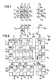
Die Matrix nach Figur 1 besteht aus den beispielsweise waagerecht verlaufenden ersten optischen Wellenleitern eWi mit i = 1 bis M und den diese ersten Wellenleiter eWi zumindest im wesentlichen senkrecht kreuzenden zweiten optischen Wellenleitern zWj mit j = 1 bis N. In jedem Kreuzungspunkt zwischen einem ersten Wellenleiter eWi und einem zweiten Wellenleiter zWj ist ein optischer Koppler Kij angeordnet, der individuell zwischen zwei Schaltzuständen schaltbar ist. Jeder dieser optischen Koppler Kij ist derart ausgebildet, daß er in einem der beiden Schaltzustände einen Leistungsanteil einer in einem der beiden in diesem Kreuzungspunkt sich kreuzenden Wellenleiter eWi und zWj geführten optischen Welle in den anderen dieser beiden Wellenleiter eWi und zWj auskoppelt, wobei wesentlich ist, daß der Auskoppelgrad dieses Kopplers Kij, d.h. das Verhältnis zwischen dem von diesem Koppler Kij ausgekoppelten Leistungsanteil zur Leistung der diesem Koppler Kij zugeführten optischen Welle gezielt gering ist, und daß der Koppler Kij in dem anderen Schaltzustand einen im Vergleich zu dem geringen Auskoppelgrad noch kleineren Auskoppelgrad aufweist.The matrix according to Figure 1 consists of, for example, horizontally extending first optical waveguides eW i with i = 1 to M and these first waveguide eW i at least substantially perpendicularly intersecting the second optical waveguides zW j with j = 1 to N. In each crossing point between A first waveguide eW i and a second waveguide zW j are arranged with an optical coupler K ij which can be switched individually between two switching states. Each of these optical couplers K ij is designed in such a way that, in one of the two switching states, it couples a power component of an optical wave guided in one of the two waveguides eW i and zW j crossing at this crossing point into the other of these two waveguides eW i and zW j , it being essential that the degree of decoupling of this coupler K ij , ie the ratio between that decoupled from this coupler K ij The proportion of power to the power of the optical wave fed to this coupler K ij is deliberately low, and that the coupler K ij in the other switching state has an even smaller degree of decoupling than the low degree of decoupling.
Geringer Auskoppelgrad bedeutet, daß dieser Auskoppelgrad zumindest größenordnungsmäßig gleich oder vorzugsweise kleiner als der Kehrwert 1/M oder 1/N der Anzahl M oder N der ersten oder zweiten Wellenleiter eWi oder zWj ist. Der noch kleinere Auskoppelgrad sollte so klein wie möglich, am besten gleich null sein. Günstig ist es auch, wenn die Durchgangsdämpfung der Wellenleiter und Koppler so klein wie möglich ist, am besten gleich null.A low degree of decoupling means that this degree of decoupling is at least of the same order of magnitude or preferably less than the reciprocal 1 / M or 1 / N of the number M or N of the first or second waveguides eW i or zW j . The even smaller degree of decoupling should be as small as possible, ideally zero. It is also favorable if the transmission loss of the waveguides and couplers is as small as possible, ideally zero.
Der gezielt geringe Auskoppelgrad hat vorteilhafterweise zur Folge, daß sich die ersten und zweiten Wellenleiter eWi und zWj unter einem sehr großen Winkel, insbesondere im Winkel von 90° kreuzen können, und daß die Koppler Kij mit extrem kurzer Koppel- oder Baulänge ausgeführt werden können, wodurch wiederum Matrizen mit extrem vielen Kopplern und extrem kleiner Ausdehnung ermöglicht werden.The deliberately low degree of decoupling advantageously has the result that the first and second waveguides eW i and zW j can cross at a very large angle, in particular at an angle of 90 °, and that the couplers K ij are designed with an extremely short coupling or installation length can be made, which in turn enables matrices with an extremely large number of couplers and extremely small dimensions.
Für die Realisierung solcher Koppler Kij mit extrem kurzer Baulänge sind die Koppler mit Mach-Zehnder-Struktur oder Richtkoppler-Struktur weniger gut oder nicht geeignet. Bei Kopplern mit Richtkoppler-Struktur könnte zwar zur Erzielung des gewünschten geringen Auskoppelgrades die eigentliche Koppelzone vernachlässigbar kurz gewählt werden, doch würde dadurch die Baulänge des Kopplers nicht wesentlich geringer, weil der Winkel zwischen den zur Koppelzone führenden Eingangswellenleitern und den von dieser Zone fortführenden Ausgangswellenleitern zur Vermeidung von durch Wellenleiterkrümmungen hervorgerufenen Verlusten nur etwa 1° beträgt.For the implementation of such couplers K ij with an extremely short overall length, the couplers with Mach-Zehnder structure or directional coupler structure are less good or not suitable. In couplers with a directional coupler structure, the actual coupling zone could be selected to be negligibly short in order to achieve the desired low degree of decoupling, but this would not significantly reduce the overall length of the coupler because the angle between the input waveguides leading to the coupling zone and the output waveguides continuing from this zone Avoidance of losses caused by waveguide curvatures is only about 1 °.
Dagegen eignen sich die Koppler mit Durchkreuzungs- oder x-Struktur zur Realisierung von Kopplern Kij mit geringem Auskoppelgrad und extrem kurzer Baulänge.In contrast, the couplers with cross-over or x structure are suitable for implementing couplers K ij with a low degree of decoupling and an extremely short overall length.
Jeder Koppler Kij der Matrix nach Figur 1 läßt beispielsweise eine im betreffenden ersten Wellenleiter eWi von links nach rechts geführte optische Welle passieren, koppelt aber in dem einen Schaltzustand einen dem geringen Auskoppelgrad entsprechenden geringen Leistungsanteil dieser optischen Welle in den betreffenden zweiten Wellenleiter zWj aus, in welchem dieser Leistungsanteil beispielsweise nach unten fortgeführt wird. Bei der Matrix nach Figur 1 koppeln insbesondere alle Koppler Kij in der gleichen Richtung aus. Z.B. wird in Bezug auf eine in der Figur 1 entsprechend den waagerechten Pfeilen von links kommende optische Welle an jedem Koppler entsprechend den vertikalen Pfeilen nach unten, eine von rechts kommende optische Welle nach oben, eine von unten kommende optische Welle nach links und eine von oben kommende optische Welle nach rechts teilweise ausgekoppelt.Each coupler K ij of the matrix according to FIG. 1 allows, for example, an optical wave guided from left to right in the first waveguide eW i in question, but in the one switching state couples a low power component of this optical wave corresponding to the low degree of decoupling into the relevant second waveguide zW j in which this share of performance is continued, for example downwards. In the matrix according to FIG. 1, all couplers K ij in particular couple out in the same direction. For example, with respect to an optical wave coming from the left in accordance with the horizontal arrows in FIG. 1, each coupler has the vertical arrows pointing downward, an optical wave coming up from the right, an optical wave coming from below to the left and one from above coming optical wave partially coupled out to the right.
In der Figur 1 sind die linken Enden der ersten Wellenleiter eWi mit Ei, die rechten Enden dieser Wellenleiter mit Ai bezeichnet. Die oberen Enden der zweiten Wellenleiter zWj sind mit E'j und die unteren Enden dieser Wellenleiter mit A'j bezeichnet. Über alle diese Enden können optische Signale in die Matrix eingekoppelt oder aus der Matrix ausgekoppelt werden. Ohne Beschränkung der Allgemeinheit sei für das folgende beispielhaft angenommen, daß die linken Enden Ei der ersten Wellenleiter eWi als Eingänge der Matrix und die unteren Enden A'j der zweiten Wellenleiter zWj als Ausgänge der Matrix benutzt werden.In Figure 1, the left ends of the first waveguides eW i with E i , the right ends of these waveguides with A i . The upper ends of the second waveguides zW j are denoted by E ' j and the lower ends of these waveguides by A' j . Optical signals can be coupled into the matrix or out of the matrix via all of these ends. Without restricting generality, it is assumed for the following by way of example that the left ends E i of the first waveguides eW i are used as inputs of the matrix and the lower ends A ' j of the second waveguides zW j are used as outputs of the matrix.
Wählt man den Auskoppelgrad der Koppler Kij der Matrix nach Figur 1 jeweils etwa 1/(kN) mit k ≧ 1, beispielsweise 1/(10N), wird erreicht, daß das Signal am Eingang jedes Kopplers Kij im ungünstigsten Fall um etwa k %, im Beispiel nur um etwa 10 % schwankt. Dies bedeutet, daß durch geeignete Wahl von k dafür gesorgt werden kann, daß jeder Koppler Kij in dem Schaltzustand mit dem geringen Auskoppelgrad der im betreffenden ersten Wellenleiter eWi geführten optischen Welle immer nur soviel Energie entnimmt, daß diese Welle energiemäßig praktisch nicht geschwächt wird und somit die Broadcasting-Funktion realisiert ist, die gleichmäßige Leistung am Eingang jedes Kopplers Kij bedeutet.If one selects the degree of decoupling of the couplers K ij of the matrix according to FIG. 1 in each case approximately 1 / (kN) with k ≧ 1, for example 1 / (10N), it is achieved that the signal at the input of each coupler K ij by approximately k %, only fluctuates by about 10% in the example. This means that by selecting k appropriately, it can be ensured that each coupler K ij in the switching state with the low degree of decoupling of the optical wave carried in the first waveguide eW i in question draws only so much energy that this wave is practically not weakened in terms of energy and thus the broadcasting function is realized, which means uniform power at the input of each coupler K ij .
Die Konzentrator-Funktion wird erhalten, weil die von den Kopplern Kij in einen zweiten Wellenleiter zWj ausgekoppelten Leistungsanteile von in den ersten Wellenleitern eWi geführten optischen Wellen auf diesem zweiten Wellenleiter zWj einem einzigen Ausgang A'j der Matrix zugeführt werden. Überdies summieren sich diese Leistungsanteile auf.The concentrator function is obtained because the power components decoupled by the couplers K ij into a second waveguide zW j of optical waves guided in the first waveguides eW i are fed to a single output A ' j of the matrix on this second waveguide zW j . In addition, these power components add up.
Zwischen irgendeinem Eingang Ei und Ausgang A'j der Matrix beträgt die Durchgangsdämpfung etwa -10log (k.N) dB, im Beispiel k = 10 also -10 log (10.N) dB, wobei N die Zahl der Ausgänge der Matrix bedeutet. Diese Dämpfung beträgt nach dem Prinzip der erfindungsgemäßen Matrix mindestens etwa -30 dB bei Verwendung elektrooptischer Materialien und mindestens etwa -20 dB bei Verwendung organischer Materialien für die Koppler Kij. Im Gegensatz dazu wächst die Durchgangsdämpfung bei einer herkömmlichen Matrix mit M Eingängen und N Ausgängen unter Verwendung herkömmlicher elektro-optischer Koppler linear mit der Zahl der passierten Kreuzungspunkte der Matrix, d.h. die Durchgangsdämpfung beträgt bei solchen Matrizen etwa (M+N) dB.The transmission loss between any input E i and output A ' j of the matrix is approximately -10log (kN) dB, in the example k = 10 thus -10 log (10.N) dB, where N is the number of outputs of the matrix. According to the principle of the matrix according to the invention, this attenuation is at least approximately -30 dB when using electro-optical materials and at least approximately -20 dB when using organic materials for the couplers K ij . In contrast, the transmission loss in a conventional matrix with M inputs and N outputs using conventional electro-optical couplers increases linearly with the number of crossing points of the matrix, ie the transmission loss in such matrices is approximately (M + N) dB.
Bei der erfindungsgemäßen Matrix nach Figur 1 beträgt bei einer Variation des Verhältnisses zwischen dem Querdurchmesser oder der Breite des Wellenleiters und der Wellenlänge der in diesem Wellenleiter geführten optischen Welle zwischen und 2 und 10 das Nebensprechen pro Kreuzungspunkt der Matrix weniger als -80 dB. Im Gegensatz dazu kann das Nebensprechen bei herkömmlichen elektrooptischen Schaltern wegen des kleinen Winkels von etwa 1° zwischen den zuführenden und den fortführenden optischen Wellenleitern je nach dem Verhältnis zwischen dem Querdurchmesser und der Breite der Wellenleiter und der Wellenlänge -20 dB bis -30 dB nicht wesentlich unterschreiten.In the matrix according to the invention according to FIG. 1, with a variation of the ratio between the transverse diameter or the width of the waveguide and the wavelength of the optical wave carried in this waveguide between 2 and 10, the crosstalk per crossing point of the matrix is less than -80 dB. In contrast, crosstalk in conventional electro-optical switches cannot be significant due to the small angle of about 1 ° between the feeding and the continuing optical waveguides depending on the ratio between the transverse diameter and the width of the waveguide and the wavelength of -20 dB to -30 dB fall below.
Der Störabstand der Matrix nach Figur 1, d.h. das Verhältnis P der Nutzleistung zur Summe aller Nebensprechleistungen auf ein und demselben zweiten Wellenleiter zWj beträgt allgemein
![]()
wobei c die Dämpfung eines nicht in den geringen Auskoppelgrad geschalteten Kopplers Kij, LD im logarithmischen Maßstab und negativ gezählt die Durchgangsdämpfung an dem in den geringen Auskoppelgrad geschalteten Koppler Kij und LM im logarithmischen Maßstab das Nebensprechen pro Koppler bedeuten.The signal-to-noise ratio of the matrix according to FIG. 1, ie the ratio P of the useful power to the sum of all crosstalk powers on one and the same second waveguide zW j is generally
![]()
where c is the attenuation of a coupler K ij , L D not switched to the low degree of decoupling on a logarithmic scale and negatively counted the transmission loss on the logarithmic scale coupler K ij and L M switched to the low degree of decoupling mean the crosstalk per coupler.
Bei einer erfindungsgemäßen Matrix nach Figur 1 kann beispielsweise c etwa 1, LD = -30 dB und LM = -80 dB angenommen werden. Mit diesen Werten beträgt für M = 10 der Störabstand P etwa 40 dB, für M = 100 beträgt P etwa 30 dB.With a matrix according to the invention according to FIG. 1, c can be assumed, for example, about 1, L D = -30 dB and L M = -80 dB. With these values, the signal-to-noise ratio P is about 40 dB for M = 10, and P is about 30 dB for M = 100.
Im Vergleich dazu gilt bei einer entsprechenden Matrix, bei denen die Koppler herkömmliche LiNbO₃-Richtkoppler sind, für c = 0,79 dB, LD = -1 dB und LN = -20 dB. Für M = 10 ergibt sich P zu etwa 4 dB, für M = 100 liegt P bei etwa -90 dB.In comparison with a corresponding matrix, in which the couplers are conventional L i NbO₃ directional couplers, applies to c = 0.79 dB, L D = -1 dB and L N = -20 dB. For M = 10, P is about 4 dB, for M = 100, P is about -90 dB.
Bei der in Figur 2 nicht maßstäblich dargestellten beispielhaften Realisierung der Matrix nach Figur 1 bestehen die ersten und zweiten Wellenleiter eWi und zWj aus auf einem gemeinsamen Substrat aus elektro-optischem Material, beispielsweise LiNbO₃, integrierten streifenartigen Wellenleitern, die in einer gemeinsamen Ebene angeordnet sind und sich in den Kreuzungspunkten zumindest im wesentlichen senkrecht schneiden. Die in diesen Kreuzungspunkten angeordneten optischen Koppler Kij bestehen jeweils aus einem elektro-optisch erzeugbaren Bragg-Gitter, dessen Gitterlinien GL zumindest im wesentlichen im Winkel von 45° zur jeweiligen Längsrichtung R₁ und R₂ der ersten und zweiten Wellenleiter eWi und zWj verlaufen und die bei allen Kopplern Kij in der gleichen Richtung R liegen. Jedes dieser Bragg-Gitter kann bekanntermaßen durch nicht dargestellte und nebeneinander in der Richtung R verlaufende streifenartige Elektroden wahlweise erzeugt werden, indem an diese Elektroden eine felderzeugende elektrische Spannung angelegt wird oder nicht (siehe dazu beispielsweise DE-OS 24 43 038 (= GR 74 P 7161 DE).In the exemplary implementation of the matrix according to FIG. 1, not shown to scale, the first and second waveguides eW i and zW j consist of strip-like waveguides integrated on a common substrate made of electro-optical material, for example L i NbO₃, which are in a common Are arranged plane and intersect at least substantially vertically at the crossing points. The arranged in these crossing points optical coupler K ij each consist of an electro-optically producible Bragg grating, the grating lines GL of which run at least substantially at an angle of 45 ° to the respective longitudinal direction R 1 and
Für eine Matrix mit M = N = 1000 und beispielsweise einem Auskoppelgrad von etwa 10⁻³ muß das Bragg-Gitter einen Beugungswirkungsgrad von 10⁻³ aufweisen. Bei LiNbO₃ ist bei einer angenommenen Vakuumwellenlänge λ₀ = 0,8 µm der optischen Welle und einem realistischen Brechzahlsprung Δn von etwa 10⁻³ für einen solchen Beugungswirkungsgrad eine Koppellänge L von nur etwa 3,7 µm erforderlich. Die Linearausdehnung einer 1000x1000 Matrix beträgt dann weniger als 10 mm.For a matrix with M = N = 1000 and, for example, an outcoupling level of approximately 10⁻³, the Bragg grating must have a diffraction efficiency of 10⁻³. At LiNbO₃ with an assumed vacuum wavelength λ₀ = 0.8 µm of the optical wave and a realistic refractive index jump Δn of about 10⁻³ for such a diffraction efficiency a coupling length L of only about 3.7 µm is required. The linear dimension of a 1000x1000 matrix is then less than 10 mm.
Generell kann angenommen werden, daß bei einer erfindungsgemäßen Matrix die Koppellänge L der optischen Koppler mit dem geringen Auskoppelgrad sehr kurz, beispielsweise 10 µm bemessen ist. Zusammen mit den im Winkel von 90° verlaufenden ersten und zweiten Wellenleitern wird bei einem Abstand zwischen den Kreuzungspunkten in der Größenordnung von 10 µm eine lineare Ausdehnung der Matrix auch bei hoher Zahl von Kreuzungspunkten extrem klein. Sie beträgt etwa 10.N µm, in herkömmlichen Matrizen dagegen mindestens 8.N mm.In general, it can be assumed that in a matrix according to the invention, the coupling length L of the optical couplers with the low degree of coupling-out is very short, for example 10 μm. Together with the first and second waveguides, which run at an angle of 90 °, a linear expansion of the matrix becomes extremely small at a distance between the crossing points of the order of magnitude of 10 μm, even with a large number of crossing points. It is about 10.N µm, in conventional matrices, however, at least 8.N mm.
Die erfindungsgemäße Matrix ist für die Realisierung künstlicher Neuronaler Netze (siehe dazu beispielsweise veröffentlichte europäische Patentanmeldung Nr. 0 349 819 A12 (= GR 88 P 1384 E) oder deutsche Patentanmeldung P 38 33 143.8 (= GR 88 P 1668 DE)) geeignet. In solchen Neuronalen Netzen spielt das Verbindungsnetzwerk der Neuronen eine entscheidende Rolle. Die Stärke dieser Verbindung repräsentiert die gespeicherte Information. In Figur 3 sind die wesentlichen Funktionsblöcke eines beispielhaften und optisch realisierbaren Neuronalen Netzes für drei Neuronen Neu1, Neu2 und Neu3 schematisch dargestellt. Eingangssignale e₁ bis e₃ werden jeweils in zugeordneten Signalaufteileinrichtungen AE1 bis AE3 leistungsmäßig aufgeteilt, die aufgeteilten Signale verschiedener Aufteileinrichtungen AE1 bis AE3 in Matrixmultiplikationseinrichtungen ME1 bis ME3 mit Matrixelementen gij multipliziert und anschließend in jeweils einem Neuron Neu1, Neu2 und Neu3 aufsummiert oder integriert und nach Maßgabe der Übertragungsfunktion des Neurons verändert. Nach einigen iterativen Schritten hat das System aus dem aus den Eingangssignalen e₁, e₂, e₃ bestehenden Eingangsmuster ein assoziiertes und aus Ausgangssignalen a₁, a₂ und a₃ bestehendes Ausgangsmuster gebildet.The matrix according to the invention is suitable for the implementation of artificial neural networks (see, for example, published European patent application No. 0 349 819 A12 (= GR 88 P 1384 E) or German patent application P 38 33 143.8 (= GR 88 P 1668 DE)). The connection network of the neurons plays a decisive role in such neural networks. The strength of this connection represents the information stored. In Figure 3, the essential functional blocks of an exemplary and optically realizable neural network for three neurons Neu1, Neu2 and Neu3 are shown schematically. Input signals e₁ to e₃ are each divided in terms of performance in assigned signal splitting devices AE1 to AE3, the divided signals of different splitting devices AE1 to AE3 are multiplied in matrix multiplication devices ME1 to ME3 by matrix elements g ij and then added or integrated in a neuron Neu1, Neu2 and Neu3 and changed in accordance with the transfer function of the neuron. After a few iterative steps, the system has formed an associated output pattern consisting of the input signals e 1,
Mathematisch entspricht die Gewichtung der Eingangssignale e₁, e₂ und e₃ oder allgemein e₁, e₂, ...eM mit den Gewichten gij und die anschließende Summation einer Multiplikation der Matrix (gij) mit dem Vektor (e₁, e₂, ... eM), die ergibt:
wobei N im Beispiel nach Figur 3 N = M = 3 ist.Mathematically, the weighting of the input signals e₁, e₂ and e₃ or generally e₁, e₂, ... e M with the weights g ij and the subsequent summation of a multiplication of the matrix (g ij ) by the vector (e₁, e₂, ... e M ), which gives:
where N in the example of FIG. 3 is N = M = 3.
Eine Einrichtung, die eine solche Matrix-Vektor-Multiplikation mit der erforderlichen Summierung leistet, sei als Synapsen-Matrix bezeichnet.A device that performs such a matrix-vector multiplication with the required summation is referred to as a synapse matrix.
Die physikalische Realisierung einer solchen Synapsen-Matrix ist für Neuronale Netze von zentraler Bedeutung. Die Synapsen-Matrix sollte außerdem optisch arbeiten, d.h., daß die einen Vektor oder ein Muster bildenden Eingangssignale e₁ bis eM und Ausgangssignale a₁ bis aN optisch vorliegen und die Verarbeitung der Eingangssignale in der Matrix optisch erfolgt.The physical implementation of such a synapse matrix is of central importance for neural networks. The synapse matrix should also work optically, ie that the input signals e 1 to e M and output signals a 1 to a N forming a vector or a pattern are present optically and the input signals in the matrix are processed optically.
Die erfindungsgemäße Matrix nach Figur 1 oder 2 ist vorteilhafterweise als optisch arbeitende Synapsen-Matrix verwendbar, da in dieser Matrix die durch die Koppler Kij in die zweiten Wellenleiter zWj ausgekoppelten Leistungsanteile sich zu einem Summensignal aufsummieren. Wegen der Reziprozität der optischen Koppler Kij wird dieses Summensignal in den betreffenden Kreuzungspunkten zwar geschwächt, aber entsprechend der Anzahl dieser Kreuzungspunkte nur gering.The matrix according to the invention according to FIG. 1 or 2 can advantageously be used as an optically operating synapse matrix, since in this matrix the power components decoupled by the couplers K ij into the second waveguide zW j add up to form a sum signal. Because of the reciprocity of the optical couplers K ij , this sum signal is weakened in the relevant intersection points, but only slightly according to the number of these intersection points.
Eine erfindungsgemäße Matrix mit M Eingängen und N Ausgängen realisiert darüber hinaus sogar ein vollständiges Neuronales Netz der Struktur nach Figur 3 mit N Neuronen für M Eingangssignale e₁ bis eM, weil aufgrund der auf den ersten Wellenleitern eWi realisierten Broadcasting-Funktion vorteilhafterweise zugleich die Signalaufteileinrichtungen AEi inhärent realisiert sind.A matrix according to the invention with M inputs and N outputs also realizes a complete neural network of the structure according to FIG. 3 with N neurons for M input signals e 1 to e M , because, due to the broadcasting function implemented on the first waveguides eW i , advantageously the signal splitting devices at the same time AEi are inherently realized.
Der Auskoppelgrad jedes Kopplers Kij sollte größenordnungsmäßig 1/(10.N) betragen, was bei 100 Ausgängen bzw. Neuronen einer Auskopplung von -30 dB bzw. einem Einfügeverlust von +30 dB entspricht.The degree of decoupling of each coupler K ij should be of the order of 1 / (10th N), which corresponds to a decoupling of -30 dB or an insertion loss of +30 dB for 100 outputs or neurons.
Das Problem der Ansteuerung der Koppler Kij kann so gelöst werden, daß die Steuerinformation jedes Kopplers Kij als Ladungsmenge auf einem diesem Koppler Kij zugeordneten Kondensator Cij, beispielsweise in FET-Ausführung, gespeichert ist, der über einen hochohmigen Ausgang praktisch unbelastet ist und die Elektroden des Kopplers Kij wahlweise speist.The problem of control of the coupler K ij can be solved so that the control information of each coupler K ij assigned as the charge amount on a this coupler K ij capacitor C ij, is stored for example in the FET embodiment, which is practically unloaded via a high-impedance output and optionally feeds the electrodes of the coupler K ij .
Auch an die Matrizen in Verteilnetzen werden die Forderungen nach geringen Einfügeverlusten, geringem Nebensprechen und kurzer Baulänge gestellt. Es sollen Signale von jedem beliebigen der M Eingänge Ei auf jeden beliebigen der N Ausgänge Aj durchgeschaltet werden. Dabei kann es erwünscht sein, daß ein Eingangssignal ei auf nur einen Ausgang Aj oder gleichzeitig auf mehrere Ausgänge geschaltet wird. Der Auskoppelgrad wird wieder 1/(10.N) gewählt. Dadurch beträgt der Einfügeverlust bei der erfindungsgemäßen Matrix etwa (10+10 log N) dB. Bei herkömmlichen Matrizen wächst der Verlust zwischen Eingang und Ausgang linear mit der Anzahl der Koppelpunkte, beträgt also (M+N) dB.The matrices in distribution networks are also subject to demands for low insertion losses, low crosstalk and short overall lengths. Signals from any of the M inputs E i are to be switched through to any of the N outputs A j . It may be desirable that an input signal e i is switched to only one output A j or to several outputs simultaneously. The degree of decoupling is again selected 1 / (10.N). As a result, the insertion loss in the matrix according to the invention is approximately (10 + 10 log N) dB. With conventional matrices, the loss between input and output increases linearly with the number of crosspoints, so it is (M + N) dB.
Auf den die Broadcasting-Funktion aufweisenden ersten Wellenleitern eWi könnten in gewissen Abständen Verstärker mit nicht linearer Kennlinie vorgesehen sein, die die Leistungspegel entlang dieser ersten Wellenleiter eWi auf einen konstanten Wert anheben. An den Ausgängen Aj der Matrix können Verstärker zum Anheben des Signalpegels vorgesehen sein.At certain intervals, amplifiers with a non-linear characteristic curve could be provided on the first waveguides eW i which have the broadcasting function and raise the power levels to a constant value along these first waveguides eW i . Amplifiers for raising the signal level can be provided at the outputs A j of the matrix.
Die beispielhafte Matrix nach Figur 4 unterscheidet sich von der beispielhaften Matrix nach Figur 2 lediglich in den Kopplern Kij, die bei der Matrix nach Figur 4 unschaltbare Koppler mit festem Auskoppelgrad sind. Zur Bildung dieser Koppler Kij weisen die ersten und zweiten optischen Wellenleiter eWi und zWj in jedem Kreuzungspunkt je einen z.B. dreieckförmigen Bereich Be mit einer Brechzahl n₁ auf, die höher ist als die Brechzahl n₀ der Wellenleiter eWi und zWj außerhalb dieser Bereiche Be. Die schräg, beispielsweise im Winkel von 45° zur Längsrichtung R1 und R2 der ersten und zweiten Wellenleiter eWi und zWj verlaufende und durch einen Brechzahlsprung von no nach n₁ definierte Grenzfläche Gfl jedes Bereiches Be definiert einen unschaltbaren Koppler Kij mit festem Auskoppelgrad.The exemplary matrix according to FIG. 4 differs from the exemplary matrix according to FIG. 2 only in the couplers K ij , which in the matrix according to FIG. 4 are non-switchable couplers with a fixed degree of decoupling. To form this coupler K ij , the first and second optical waveguides eW i and zW j each have, for example, a triangular region Be with a refractive index n ₁ that is higher than the refractive index n₀ of the waveguides eW i and zW j outside of these regions Be. The oblique, for example at an angle of 45 ° to the longitudinal direction R1 and R2 of the first and second waveguides eW i and zW j and defined by a refractive index jump from n o to n₁ defined interface Gfl each area Be defines a non-switchable coupler K ij with a fixed degree of decoupling.
Jeder Bereich Be kann beispielsweise durch Ionenaustausch, z.B. durch Li-Austausch gegen H₂ in LiNbO₃ hergestellt werden, wobei Brechzahlunterschiede Δn = n₁-n₀ bis zu 10⁻¹ erreicht werden können. Auch mit Ionenimplantation können Brechzahlunterschiede Δn bis zu 10⁻¹ erhalten werden. Durch Steuerung von Δn und/oder der Eindringtiefe der Ionen läßt sich der gewünschte Auskoppelgrad festlegen.Each area Be can e.g. by ion exchange, e.g. can be produced by Li exchange for H₂ in LiNbO₃, where refractive index differences Δn = n₁-n₀ up to 10⁻¹ can be achieved. Refractive index differences Δn of up to 10⁻¹ can also be obtained with ion implantation. The desired degree of coupling-out can be determined by controlling Δn and / or the penetration depth of the ions.
Die Matrix nach Figur 4 kann beispielsweise als optischer Mischer oder Sternkoppler verwendet werden, wobei die Auskoppelgrade der unschaltbaren Koppler so gering gewählt werden, daß jedes der zu mischenden Eingangssignale e₁ bis eM sich auf dem horizontalen Weg des ihm zugeordneten ersten Wellenleiters eWi nur gering, z.B. 10 % geschwächt wird. Durch diesen geringen Auskoppelgrad wird auch die zweite Forderung erfüllt, daß die in einen vertikalen zweiten Wellenleiter zWj ausgekoppelten und zu dem diesem Wellenleiter zugeordneten Ausgang A'j aufsummierten Lichtanteile auch nur gering, z.B. schlechtestenfalls um 10 % geschwächt werden, wobei dies für jeden zweiten Wellenleiter zWj und den ihm zugeordneten Ausgang A'j gilt. Die zu mischenden Eingangssignale e₁ bis eM werden beispielsweise parallel an die Eingänge E₁ bis En gegeben, während die gemischten Ausgangssignale a₁ bis aN den Ausgängen A'₁ bis A'N entnommen werden können.The matrix according to FIG. 4 can be used, for example, as an optical mixer or star coupler, the coupling levels of the non-switchable couplers being chosen so low that each of the input signals e 1 to e M to be mixed is only slight on the horizontal path of the first waveguide eW i assigned to it , for example 10% is weakened. This low degree of decoupling also fulfills the second requirement that the light components which are coupled out into a vertical second waveguide zW j and added up to the output A ' j assigned to this waveguide are only slightly weakened, for example at worst by 10%, this being the case for every second Waveguide zW j and the output A ' j assigned to it apply. The input signals to be mixed e₁ to e M are, for example, given in parallel to the inputs E₁ to E n , while the mixed output signals a₁ to a N the outputs A'₁ to A ' N can be removed.
Die Ähnlichkeit der Matrizen nach den Figuren 2 und 4 ermöglicht auch die einfache und billige Realisierung von winzigen optischen Matrizen mit einer Vielzahl von optischen Kopplern, bei denen anwendungsbedingt sowohl schaltbare Koppler mit geringem Ankoppelgrad als auch unschaltbare Koppler mit festem Ankoppelgrad vorhanden sind, wobei in einer Matrix auch beide Kopplerarten realisiert sein können.The similarity of the matrices according to FIGS. 2 and 4 also enables the simple and inexpensive realization of tiny optical matrices with a large number of optical couplers, in which, depending on the application, both switchable couplers with a low degree of coupling and non-switchable couplers with a fixed degree of coupling are present, in one Matrix, both types of couplers can also be implemented.
Claims (13)
dadurch gekennzeichnet, daß
characterized in that
Applications Claiming Priority (2)
| Application Number | Priority Date | Filing Date | Title |
|---|---|---|---|
| DE4007976 | 1990-03-13 | ||
| DE4007976 | 1990-03-13 |
Publications (2)
| Publication Number | Publication Date |
|---|---|
| EP0446437A2 true EP0446437A2 (en) | 1991-09-18 |
| EP0446437A3 EP0446437A3 (en) | 1992-10-28 |
Family
ID=6402096
Family Applications (1)
| Application Number | Title | Priority Date | Filing Date |
|---|---|---|---|
| EP19900123235 Ceased EP0446437A3 (en) | 1990-03-13 | 1990-12-04 | Optical matrix |
Country Status (1)
| Country | Link |
|---|---|
| EP (1) | EP0446437A3 (en) |
Cited By (3)
| Publication number | Priority date | Publication date | Assignee | Title |
|---|---|---|---|---|
| EP0615390A2 (en) * | 1993-03-09 | 1994-09-14 | Hitachi, Ltd. | Optical switch, optical matrix switch system and method of optimizing system connectivity |
| DE19702743A1 (en) * | 1997-01-15 | 1998-07-23 | Siemens Ag | Integrated optical switching circuit |
| EP0876069A1 (en) * | 1997-05-02 | 1998-11-04 | Alcatel | Switch network |
Citations (1)
| Publication number | Priority date | Publication date | Assignee | Title |
|---|---|---|---|---|
| FR2429445A1 (en) * | 1978-06-20 | 1980-01-18 | Favre Francois | INTEGRATED ELECTRO-OPTICAL CIRCUIT FOR THE SWITCHING OF OPTICALLY ROUTED SIGNALS |
-
1990
- 1990-12-04 EP EP19900123235 patent/EP0446437A3/en not_active Ceased
Patent Citations (1)
| Publication number | Priority date | Publication date | Assignee | Title |
|---|---|---|---|---|
| FR2429445A1 (en) * | 1978-06-20 | 1980-01-18 | Favre Francois | INTEGRATED ELECTRO-OPTICAL CIRCUIT FOR THE SWITCHING OF OPTICALLY ROUTED SIGNALS |
Non-Patent Citations (2)
| Title |
|---|
| APPLIED OPTICS. Bd. 26, Nr. 23, 1. Dezember 1987, NEW YORK US Seiten 5031 - 5038; D.Z. ANDERSON ET AL: 'Dynamic optical interconnects: volume holograms as optical two-port operators' * |
| IBM TECHNICAL DISCLOSURE BULLETIN. Bd. 13, Nr. 9, Februar 1971, NEW YORK US Seiten 2708 - 2709; F.P. CARTMAN ET AL: 'Three Stage Switching with Preconfigured Center Stage Subswitches' * |
Cited By (6)
| Publication number | Priority date | Publication date | Assignee | Title |
|---|---|---|---|---|
| EP0615390A2 (en) * | 1993-03-09 | 1994-09-14 | Hitachi, Ltd. | Optical switch, optical matrix switch system and method of optimizing system connectivity |
| EP0615390A3 (en) * | 1993-03-09 | 1995-10-25 | Hitachi Ltd | Optical switch, optical matrix switch system and method of optimizing system connectivity. |
| US5790290A (en) * | 1993-03-09 | 1998-08-04 | Hitachi, Ltd. | Optical distribution system having time switch |
| DE19702743A1 (en) * | 1997-01-15 | 1998-07-23 | Siemens Ag | Integrated optical switching circuit |
| EP0876069A1 (en) * | 1997-05-02 | 1998-11-04 | Alcatel | Switch network |
| FR2762948A1 (en) * | 1997-05-02 | 1998-11-06 | Alsthom Cge Alcatel | SWITCH NETWORK |
Also Published As
| Publication number | Publication date |
|---|---|
| EP0446437A3 (en) | 1992-10-28 |
Similar Documents
| Publication | Publication Date | Title |
|---|---|---|
| DE69120479T2 (en) | ELECTRIC FIELD INDUCED QUANTUM POTENTIAL POT WAVE GUIDE | |
| EP0782809B1 (en) | Tree-structured optical 1xn and nxn switch matrices | |
| DE3209927C2 (en) | ||
| DE69523104T2 (en) | PHASE COUPLED OPTICAL DEVICE | |
| EP0662621B1 (en) | Optical device having strip optical waveguides | |
| DE60010053T2 (en) | ELECTRICALLY ADJUSTABLE LOAD GRID | |
| EP0985159B1 (en) | Integrated optical circuit | |
| EP0840900B1 (en) | Optical structure and method for its production | |
| DE1639269C3 (en) | Device for the controllable deflection of a light beam containing several wavelengths | |
| DE69704642T2 (en) | Optical wavelength multiplexer / demultiplexer | |
| DE2443038C2 (en) | Electro-optical switch and modulator for intersecting or branching optical waveguides | |
| DE69013130T2 (en) | Optical spatial switch and network with such optical spatial switches. | |
| DE2804105C2 (en) | ||
| DE3883492T2 (en) | Method for arranging a polarization-directing optoelectronic switch and a switch therefor. | |
| EP1070271B1 (en) | Arrangement for spatial separation and/or convergence of optical wavelength channels | |
| DE69810509T2 (en) | Device and method for spatially splitting the frequency components of incident optical radiation | |
| DE69418798T2 (en) | Active optical semiconductor ridge waveguide element | |
| DE69216299T2 (en) | Directional coupler optical device and control method therefor | |
| DE3101415C2 (en) | ||
| DE69421477T2 (en) | Optical waveguide device | |
| DE3881138T2 (en) | OPTICAL SWITCHING ELEMENT MADE OF TWO PARALLEL LIGHT GUIDES AND SWITCHING MATRIX COMPOSED FROM SUCH ELEMENTS. | |
| EP0704946A1 (en) | Optoelectronic multiwavelength construction element | |
| DE69105614T2 (en) | Digital optical switch. | |
| EP0446437A2 (en) | Optical matrix | |
| DE2619327A1 (en) | ELECTRO-OPTICAL SWITCH |
Legal Events
| Date | Code | Title | Description |
|---|---|---|---|
| PUAI | Public reference made under article 153(3) epc to a published international application that has entered the european phase |
Free format text: ORIGINAL CODE: 0009012 |
|
| 17P | Request for examination filed |
Effective date: 19901220 |
|
| AK | Designated contracting states |
Kind code of ref document: A2 Designated state(s): AT BE CH DE FR GB IT LI NL SE |
|
| PUAL | Search report despatched |
Free format text: ORIGINAL CODE: 0009013 |
|
| AK | Designated contracting states |
Kind code of ref document: A3 Designated state(s): AT BE CH DE FR GB IT LI NL SE |
|
| 17Q | First examination report despatched |
Effective date: 19951102 |
|
| STAA | Information on the status of an ep patent application or granted ep patent |
Free format text: STATUS: THE APPLICATION HAS BEEN REFUSED |
|
| 18R | Application refused |
Effective date: 20011029 |