EP0445826B1 - Sequential logic circuit device - Google Patents
Sequential logic circuit device Download PDFInfo
- Publication number
- EP0445826B1 EP0445826B1 EP91103522A EP91103522A EP0445826B1 EP 0445826 B1 EP0445826 B1 EP 0445826B1 EP 91103522 A EP91103522 A EP 91103522A EP 91103522 A EP91103522 A EP 91103522A EP 0445826 B1 EP0445826 B1 EP 0445826B1
- Authority
- EP
- European Patent Office
- Prior art keywords
- flip
- flop
- signal
- circuit
- gate
- Prior art date
- Legal status (The legal status is an assumption and is not a legal conclusion. Google has not performed a legal analysis and makes no representation as to the accuracy of the status listed.)
- Expired - Lifetime
Links
Images


Classifications
-
- H—ELECTRICITY
- H03—ELECTRONIC CIRCUITRY
- H03K—PULSE TECHNIQUE
- H03K19/00—Logic circuits, i.e. having at least two inputs acting on one output; Inverting circuits
-
- G—PHYSICS
- G05—CONTROLLING; REGULATING
- G05B—CONTROL OR REGULATING SYSTEMS IN GENERAL; FUNCTIONAL ELEMENTS OF SUCH SYSTEMS; MONITORING OR TESTING ARRANGEMENTS FOR SUCH SYSTEMS OR ELEMENTS
- G05B19/00—Program-control systems
- G05B19/02—Program-control systems electric
- G05B19/04—Program control other than numerical control, i.e. in sequence controllers or logic controllers
- G05B19/042—Program control other than numerical control, i.e. in sequence controllers or logic controllers using digital processors
- G05B19/0423—Input/output
-
- G—PHYSICS
- G01—MEASURING; TESTING
- G01R—MEASURING ELECTRIC VARIABLES; MEASURING MAGNETIC VARIABLES
- G01R31/00—Arrangements for testing electric properties; Arrangements for locating electric faults; Arrangements for electrical testing characterised by what is being tested not provided for elsewhere
- G01R31/28—Testing of electronic circuits, e.g. by signal tracer
- G01R31/317—Testing of digital circuits
- G01R31/3181—Functional testing
- G01R31/3185—Reconfiguring for testing, e.g. LSSD, partitioning
- G01R31/318533—Reconfiguring for testing, e.g. LSSD, partitioning using scanning techniques, e.g. LSSD, Boundary Scan, JTAG
- G01R31/318541—Scan latches or cell details
-
- H—ELECTRICITY
- H03—ELECTRONIC CIRCUITRY
- H03K—PULSE TECHNIQUE
- H03K3/00—Circuits for generating electric pulses; Monostable, bistable or multistable circuits
- H03K3/02—Generators characterised by the type of circuit or by the means used for producing pulses
- H03K3/26—Generators characterised by the type of circuit or by the means used for producing pulses by the use, as active elements, of bipolar transistors with internal or external positive feedback
- H03K3/28—Generators characterised by the type of circuit or by the means used for producing pulses by the use, as active elements, of bipolar transistors with internal or external positive feedback using means other than a transformer for feedback
- H03K3/281—Generators characterised by the type of circuit or by the means used for producing pulses by the use, as active elements, of bipolar transistors with internal or external positive feedback using means other than a transformer for feedback using at least two transistors so coupled that the input of one is derived from the output of another, e.g. multivibrator
- H03K3/284—Generators characterised by the type of circuit or by the means used for producing pulses by the use, as active elements, of bipolar transistors with internal or external positive feedback using means other than a transformer for feedback using at least two transistors so coupled that the input of one is derived from the output of another, e.g. multivibrator monostable
Definitions
- the present invention relates to a sequential logic circuit device which is used in, for example, a computer BIOS controller.
- Logic circuits can be classified into a sequential logic circuit which includes flip-flops or similar storage circuits, and a combinational circuit of logic elements (such as an AND, an OR and an INV) which does not include the above-mentioned storage circuits.
- the sequential logic circuit is composed of pluralities of flip-flops and logic elements intermingled and interconnected as desired but it can be regarded as being made up of a flip-flop group and a logic element combinational circuit connected thereto.
- the internal storage state of the sequential logic circuit (such as a shift register) usually varies with each operation clock, even if input data remains intact.
- the number of internal storage states increases with enlargement of the circuit scale.
- the generation of a test pattern of a high fault detection ratio for circuit testing use is far more difficult than in the case of testing combinational circuits.
- a scan design system has been proposed as a solution to this problem (Ando, H., "Testing VLSI with Random Access Scan,” Compcon, Spring 80, Digest of Papers, pp. 50-52, Feb. 1980, for example).
- a problem for testing the sequential operation type logic circuit can be solved as a problem for testing the combinational circuit by additionally providing a scan circuit for setting and observing directly from the outside the internal state of the flip-flop group capable of storing a number of logical operation states.
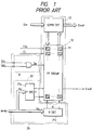
- Fig. 1 shows an example of the sequential logic circuit in which a logic circuit part 10 having an intended function is added with a scan circuit 20 for testing use, based on the conventional scan design system.
- the logic circuit part 10 is shown to be divided into a combinational circuit 12 and a flip-flop group 11 composed of a plurality of flip-flops FC for the sake of convenience.
- the scan circuit 20 is made up of a write circuit 21 and a specify circuit 22. Based on decoded addresses X and Y obtained by decoding a scan address (AxAy) with an X decoder 21x and a Y decoder 21y, the specify circuit 22 selectively specifies one of flip-flop circuits FC in the flip-flop group 11.
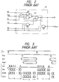
- each flip-flop circuit FC has such a construction as shown in Fig. 2, for example.
- a system clock Csy and a clear signal CL can be provided in common to all of the flip-flop circuits FC.
- input data di from the combinational circuit 12 is loaded by the system clock Csy into a flip-flop FF via a gate G2 and its output data do is applied to the combinational circuit 12.
- This construction is to implement the intended function of the logic circuit part 10.
- each flip-flop circuit FC includes gates G1 and G3, which are enabled by the decoded addresses X and Y which are provided from the specify circuit 22 for selecting the flip-flop circuit FC.
- a scan set signal Ss from the write circuit 21 is provided via the gate G1 of the selected flip-flop circuit FC to the flip-flop FF to set it.
- the output logic state of the flip-flop FF of the selected flip-flop circuit FC can be directly taken out of the logic circuit part 10, as a scan out signal Sout, via the gate G3.
- the output logic state of this flip-flop FF will also be referred to as the output logic state of the flip-flop circuit FC.
- the scan circuit 20 In the normal operation of the logic circuit part 10 as an ordinary logic circuit the scan circuit 20 is inoperative and the logic circuit part 10 performs the intended logical operation based on a system input data Din and the system clock Csy and provides system output data Dout.
- the testing of the logic circuit part 10 starts with initializing the flip-flop FF of every flip-flop circuit FC in the flip-flop group 11 to a "0" by the clear signal CL as shown in Fig. 3.
- a series of scan addresses (AxAy) for specifying flip-flops FF to be set to a "1" in the period T1 are sequentially applied to the specify circuit 22 and, at the same time, a scan-in signal Sin and a scan clock Csc are applied to the write circuit 21, by which scan set signals Ss are sequentially provided to the flip-flop circuits FC specified by the scan addresses AxAy.
- predetermined system input data Din is applied to the logic circuit part 10 and, at the same time, one system clock Csy is provided, by which a transition is made in the internal state of the logic circuit part 10.
- a series of scan addresses (AxAy) for specifying the flip-flops FF are sequentially applied to the specify circuit 22 in period T2 and output logic states of the specified flip-flops FF are sequentially read out as scan-out signals Sout.
- the system output data Dout after the state transition is also obtained.
- the clear signal CL is applied again to all the flip-flop circuits FC to initialize them and then the application of the scan set signal Ss to the flip-flop circuits FC, the transition of the internal state of the logic circuit part 10 by the system clock Csy and the readout of the scan-out signal Sout are repeated in the same manner as described above.
- the conventional circuit arrangement always needs to apply the clear signal CL to the flip-flop group 11 prior to not only the first but each setting thereof on and after the second time by the scan circuit 20, and consequently, those of the flip-flops FF which have already been set and need not be reset will also be reset by the clear signal CL.
- the states of all the flip-flops FF in the flip-flop group 11 must be set again -- this inevitably increases the time T1 needed for setting the flip-flops FF on and after the second time.
- Fig. 4 illustrates the construction of the sequential logic circuit device according to the present invention.
- This embodiment is identical with the prior art example of Fig. 1 in the provision of the combinational circuit 12 and the flip-flop group 11 in the logic circuit part 10 and the scan circuit 20 but differs from the prior art in the constructions of each flip-flop circuit FC forming the flip-flop group 11 and the write circuit 21 forming the scan circuit 20 as described below.
- the write circuit 21 which forms the scan circuit 20 is constructed so that it can freely set a "0" or "1" in a desired one or ones of the flip-flops in the flip-flop group 11.
- the write circuit 21 is made up of two AND gates 21A and 21B and an inverter 21C and the scan-in signal Sin is applied to the one input terminal of the gate 21B and via the inverter 21C to the one input terminal of the gate 21A.
- the scan clock Csc is provided to the other input terminals of the gates 21A and 21B.
- the scan clock Csc is provided, as the scan set signal Ss, via the gate 21B to all of the flip-flop circuits FC in the flip-flop group 11, and a "1" is written into that one of the flip-flop circuits FC which is being specified by the specify circuit 22 at this time.
- the gate 21B When the scan-in signal Sin is switched to a "0", the gate 21B is disabled but instead the gate 21A is enabled. Consequently, in this instance the scan clock Csc is provided, as a scan reset signal Rs, via the gate 21A to all the flip-flop circuits FC in the flip-flop group 11, and a "0" is written into that one of the flip-flop circuits FC which is being specified by the specify circuit 22 at this time.
- Fig. 5 illustrates the construction of each flip-flop circuit FC which is provided in the flip-flop group 11.
- the flip-flop circuit FC is shown to be composed of a D type flip-flop DFF provided with a set input terminal S and a reset input terminal R, three AND gates G1, G2 and G3 which are enabled when the decoded addresses X and Y both match a "1", that is, when the flip-flop circuit FC is specified by the specify circuit 22, and one OR gate OR.
- the gate G1 is enabled when the decoded addresses X and Y both go to a "1", and if the scan set signal Ss mentioned above in respect of Fig. 4 is input at this time, it is provided to the set input terminal S of the D type flip-flop DFF, by which the flip-flop DFF is set and a "1" is written thereinto.
- the scan reset signal Rs is input into the gate G2 when the decoded addresses X and Y are both at the "1" level, the scan reset signal Rs is applied to the reset terminal R of the D type flip-flop DFF via the gate G2 and the OR gate OR, by which the D type flip-flop DFF is reset and a "0" is written thereinto.
- whether the scan set signal Ss or the scan reset signal Rs is input as mentioned above is dependent on whether the scan-in signal Sin which is provided to the write circuit 21 is a "1" or "0".
- the output logic state (a Q output) of the D type flip-flop DFF is directly output, as the scan-out signal Sout, to the outside of the logic circuit part 10. Since the gates G1 and G2 are also enabled together with the gate G3, the result of the write (set or reset) in the D flip-flop DFF can be read out at the same time as the write is effected in the flip-flop DFF, and the logic state of a desired one of the flip-flops can also be read out.
- the first step is to initialize the flip-flops DFF of all the flip-flop circuits FC in the flip-flop group 11 to the "0" level by the clear signal CL as shown in Fig. 6.
- a sequence of scan addresses (AxAy) for specifying a flip-flop or flip-flops DFF to be set to a logic level "1" is to be set in the period T1 are sequentially applied to the specify circuit 22 from the outside, and at the same time, the scan-in signal Sin and the scan clock Csc are provided to the write circuit 21, which, in turn, outputs the scan set signal Ss or scan reset signal RS to all the flip-flops DFF so that the set signal Ss or reset signal Rs is written into a flip-flop or flip-flops specified by the scan address (AxAy).
- the scan address (AxAy) In the first state setting period, i.e.
- a sequence of scan addresses AxAy for specifying flip-flops DFF to read out are sequentially applied to the specify circuit 22 and the output logic states of the specified flip-flops DFF are sequentially read out as the scan out signal Sout.
- the procedure to this point is substantially the same as that adopted by the prior art example shown in Fig. 3.
- the device of the present invention has a striking feature appearing in the following procedure.
- the second scan write needs to write a "1" or "0” into only those of the flip-flops DFF which differ in logic between the internal state of the logic circuit part 10 to be set and its current internal state. Therefore, the second scan write can immediately be effected without the necessity of applying the clear signal CL to the logic circuit part 10. Moreover, as the number of flip-flops DFF to be written decreases, the scan write period T1 decreases accordingly. The same is true of the third and subsequent scan write periods T1.
- the state of desired one or ones of the flip-flops in the flip-flop group 11 can be read out and a "0" or "1" can selectively be written into the desired flip-flop or flip-flops.
Landscapes
- Engineering & Computer Science (AREA)
- Physics & Mathematics (AREA)
- General Physics & Mathematics (AREA)
- General Engineering & Computer Science (AREA)
- Automation & Control Theory (AREA)
- Computer Hardware Design (AREA)
- Computing Systems (AREA)
- Mathematical Physics (AREA)
- Power Engineering (AREA)
- Tests Of Electronic Circuits (AREA)
- Test And Diagnosis Of Digital Computers (AREA)
- Electronic Switches (AREA)
Description
- The present invention relates to a sequential logic circuit device which is used in, for example, a computer BIOS controller.
- Logic circuits can be classified into a sequential logic circuit which includes flip-flops or similar storage circuits, and a combinational circuit of logic elements (such as an AND, an OR and an INV) which does not include the above-mentioned storage circuits. The sequential logic circuit is composed of pluralities of flip-flops and logic elements intermingled and interconnected as desired but it can be regarded as being made up of a flip-flop group and a logic element combinational circuit connected thereto.
- The internal storage state of the sequential logic circuit (such as a shift register) usually varies with each operation clock, even if input data remains intact. In addition, the number of internal storage states increases with enlargement of the circuit scale. On this account, the generation of a test pattern of a high fault detection ratio for circuit testing use is far more difficult than in the case of testing combinational circuits.
- A scan design system has been proposed as a solution to this problem (Ando, H., "Testing VLSI with Random Access Scan," Compcon, Spring 80, Digest of Papers, pp. 50-52, Feb. 1980, for example). According to this conventional system, a problem for testing the sequential operation type logic circuit can be solved as a problem for testing the combinational circuit by additionally providing a scan circuit for setting and observing directly from the outside the internal state of the flip-flop group capable of storing a number of logical operation states. By fabricating, for example, as one IC, sequential logic circuit devices each provided with the scan circuit which permits testing of the sequential logic circuit having primarily intended functions, each circuit device can easily be tested.
- Fig. 1 shows an example of the sequential logic circuit in which a
logic circuit part 10 having an intended function is added with ascan circuit 20 for testing use, based on the conventional scan design system. This example is cited from the above-mentioned literature. Thelogic circuit part 10 is shown to be divided into acombinational circuit 12 and a flip-flop group 11 composed of a plurality of flip-flops FC for the sake of convenience. Thescan circuit 20 is made up of awrite circuit 21 and aspecify circuit 22. Based on decoded addresses X and Y obtained by decoding a scan address (AxAy) with anX decoder 21x and aY decoder 21y, thespecify circuit 22 selectively specifies one of flip-flop circuits FC in the flip-flop group 11. - For testing the
logic circuit part 10 according to the scan design system, each flip-flop circuit FC has such a construction as shown in Fig. 2, for example. A system clock Csy and a clear signal CL can be provided in common to all of the flip-flop circuits FC. In each flip-flop circuit FC input data di from thecombinational circuit 12 is loaded by the system clock Csy into a flip-flop FF via a gate G2 and its output data do is applied to thecombinational circuit 12. This construction is to implement the intended function of thelogic circuit part 10. In order that thelogic circuit part 10 may be tested according to the scan design system, each flip-flop circuit FC includes gates G1 and G3, which are enabled by the decoded addresses X and Y which are provided from thespecify circuit 22 for selecting the flip-flop circuit FC. A scan set signal Ss from thewrite circuit 21 is provided via the gate G1 of the selected flip-flop circuit FC to the flip-flop FF to set it. The output logic state of the flip-flop FF of the selected flip-flop circuit FC can be directly taken out of thelogic circuit part 10, as a scan out signal Sout, via the gate G3. In the following description the output logic state of this flip-flop FF will also be referred to as the output logic state of the flip-flop circuit FC. - In the normal operation of the
logic circuit part 10 as an ordinary logic circuit thescan circuit 20 is inoperative and thelogic circuit part 10 performs the intended logical operation based on a system input data Din and the system clock Csy and provides system output data Dout. - The testing of the
logic circuit part 10 starts with initializing the flip-flop FF of every flip-flop circuit FC in the flip-flop group 11 to a "0" by the clear signal CL as shown in Fig. 3. Next, a series of scan addresses (AxAy) for specifying flip-flops FF to be set to a "1" in the period T₁ are sequentially applied to thespecify circuit 22 and, at the same time, a scan-in signal Sin and a scan clock Csc are applied to thewrite circuit 21, by which scan set signals Ss are sequentially provided to the flip-flop circuits FC specified by the scan addresses AxAy. Then, after predetermined flip-flop circuits FC have each been set to a predetermined logic state in the period T₁, predetermined system input data Din is applied to thelogic circuit part 10 and, at the same time, one system clock Csy is provided, by which a transition is made in the internal state of thelogic circuit part 10. For checking whether or not the internal state after the transition is an expected logic state, a series of scan addresses (AxAy) for specifying the flip-flops FF are sequentially applied to thespecify circuit 22 in period T₂ and output logic states of the specified flip-flops FF are sequentially read out as scan-out signals Sout. At this time, the system output data Dout after the state transition is also obtained. Thereafter, the clear signal CL is applied again to all the flip-flop circuits FC to initialize them and then the application of the scan set signal Ss to the flip-flop circuits FC, the transition of the internal state of thelogic circuit part 10 by the system clock Csy and the readout of the scan-out signal Sout are repeated in the same manner as described above. - As will be seen from the above, the conventional circuit arrangement always needs to apply the clear signal CL to the flip-
flop group 11 prior to not only the first but each setting thereof on and after the second time by thescan circuit 20, and consequently, those of the flip-flops FF which have already been set and need not be reset will also be reset by the clear signal CL. Hence, the states of all the flip-flops FF in the flip-flop group 11 must be set again -- this inevitably increases the time T₁ needed for setting the flip-flops FF on and after the second time. - It is therefore an object of the present invention to provide a sequential logic circuit device which permits quick setting of the states of flip-flops of the logic circuit part.
- This object is achieved with a sequential logic circuit as claimed in claim 1.
- Preferred embodiments of the invention are subject-matter of the dependent claims.
- With the circuit structure of the present invention, a "0" or "1" can freely be written into each flip-flop of the flip-flop group, besides the state of the flip-flop can freely be read out. Hence, the logic state of each flip-flop in the flip-flop group can be detected from the outside and only those of the flip-flops whose logic states must be changed can be accessed from the outside for rewriting their logic states. This affords reduction of the time for initialization in the case of testing, and consequently, shortens the time for testing.
-
- Fig. 1 is a block diagram for explaining a conventional sequential logic circuit device;
- Fig. 2 is a connection diagram for explaining the concrete structure of a flip-flop circuit for use in the device depicted in Fig. 1;
- Fig. 3 is timing chart for explaining the operation of the device shown in Fig. 1;
- Fig. 4 is a block diagram illustrating an embodiment of the sequential logic circuit device of the present invention;
- Fig. 5 is a connection diagram showing an example of the concrete structure of the flip-flop circuit for use in the embodiment of Fig. 4; and
- Fig. 6 is a timing chart for explaining the operation of the device illustrated in Fig. 4.
- Fig. 4 illustrates the construction of the sequential logic circuit device according to the present invention. This embodiment is identical with the prior art example of Fig. 1 in the provision of the
combinational circuit 12 and the flip-flop group 11 in thelogic circuit part 10 and thescan circuit 20 but differs from the prior art in the constructions of each flip-flop circuit FC forming the flip-flop group 11 and thewrite circuit 21 forming thescan circuit 20 as described below. - In the present invention the
write circuit 21 which forms thescan circuit 20 is constructed so that it can freely set a "0" or "1" in a desired one or ones of the flip-flops in the flip-flop group 11. In this embodiment thewrite circuit 21 is made up of twoAND gates inverter 21C and the scan-in signal Sin is applied to the one input terminal of thegate 21B and via theinverter 21C to the one input terminal of thegate 21A. The scan clock Csc is provided to the other input terminals of thegates gate 21A is disabled, whereas thegate 21B is enabled. As a result of this, the scan clock Csc is provided, as the scan set signal Ss, via thegate 21B to all of the flip-flop circuits FC in the flip-flop group 11, and a "1" is written into that one of the flip-flop circuits FC which is being specified by thespecify circuit 22 at this time. - When the scan-in signal Sin is switched to a "0", the
gate 21B is disabled but instead thegate 21A is enabled. Consequently, in this instance the scan clock Csc is provided, as a scan reset signal Rs, via thegate 21A to all the flip-flop circuits FC in the flip-flop group 11, and a "0" is written into that one of the flip-flop circuits FC which is being specified by thespecify circuit 22 at this time. - Fig. 5 illustrates the construction of each flip-flop circuit FC which is provided in the flip-
flop group 11. The flip-flop circuit FC is shown to be composed of a D type flip-flop DFF provided with a set input terminal S and a reset input terminal R, three AND gates G1, G2 and G3 which are enabled when the decoded addresses X and Y both match a "1", that is, when the flip-flop circuit FC is specified by thespecify circuit 22, and one OR gate OR. - The gate G1 is enabled when the decoded addresses X and Y both go to a "1", and if the scan set signal Ss mentioned above in respect of Fig. 4 is input at this time, it is provided to the set input terminal S of the D type flip-flop DFF, by which the flip-flop DFF is set and a "1" is written thereinto.
- On the other hand, if the scan reset signal Rs is input into the gate G2 when the decoded addresses X and Y are both at the "1" level, the scan reset signal Rs is applied to the reset terminal R of the D type flip-flop DFF via the gate G2 and the OR gate OR, by which the D type flip-flop DFF is reset and a "0" is written thereinto. Incidentally, whether the scan set signal Ss or the scan reset signal Rs is input as mentioned above is dependent on whether the scan-in signal Sin which is provided to the
write circuit 21 is a "1" or "0". - When the gate G3 is enabled, the output logic state (a Q output) of the D type flip-flop DFF is directly output, as the scan-out signal Sout, to the outside of the
logic circuit part 10. Since the gates G1 and G2 are also enabled together with the gate G3, the result of the write (set or reset) in the D flip-flop DFF can be read out at the same time as the write is effected in the flip-flop DFF, and the logic state of a desired one of the flip-flops can also be read out. - For testing the
logic circuit part 10 of the device of the present invention shown in Fig. 4, the first step is to initialize the flip-flops DFF of all the flip-flop circuits FC in the flip-flop group 11 to the "0" level by the clear signal CL as shown in Fig. 6. Next, a sequence of scan addresses (AxAy) for specifying a flip-flop or flip-flops DFF to be set to a logic level "1" is to be set in the period T₁ are sequentially applied to thespecify circuit 22 from the outside, and at the same time, the scan-in signal Sin and the scan clock Csc are provided to thewrite circuit 21, which, in turn, outputs the scan set signal Ss or scan reset signal RS to all the flip-flops DFF so that the set signal Ss or reset signal Rs is written into a flip-flop or flip-flops specified by the scan address (AxAy). (In the first state setting period, i.e. in the scan write period T₁, however, since all the flip-flops DFF have been initialized to the "0" state by the clear signal CL, a "1" needs only to be written into a desired one or ones of the flip-flops DFF and only the scan set signal Ss needs to be generated.) Next, predetermined system input data Din is provided to thelogic circuit part 10, and at the same time, one shot of the system clock Csy is applied to thelogic circuit part 10 to cause a transition of its internal state. To check whether or not the internal state after the transition is an expected logic state, a sequence of scan addresses AxAy for specifying flip-flops DFF to read out are sequentially applied to the specifycircuit 22 and the output logic states of the specified flip-flops DFF are sequentially read out as the scan out signal Sout. The procedure to this point is substantially the same as that adopted by the prior art example shown in Fig. 3. The device of the present invention has a striking feature appearing in the following procedure. That is, according to the construction of the device of the present invention, since anyone of the flip-flops DFF can be specified and either "1" or "0" can be written into the specified flip-flop, the second scan write needs to write a "1" or "0" into only those of the flip-flops DFF which differ in logic between the internal state of thelogic circuit part 10 to be set and its current internal state. Therefore, the second scan write can immediately be effected without the necessity of applying the clear signal CL to thelogic circuit part 10. Moreover, as the number of flip-flops DFF to be written decreases, the scan write period T₁ decreases accordingly. The same is true of the third and subsequent scan write periods T₁. - As described above, according to the present invention, the state of desired one or ones of the flip-flops in the flip-
flop group 11 can be read out and a "0" or "1" can selectively be written into the desired flip-flop or flip-flops. - Thus, there is no need to reset all the flip-flops in the flip-
flop group 11 by the clear signal CL prior to the initialization thereof by the scan write as in the prior art, and the write needs to be effected in only those of the flip-flops which are desired to change their logic state, and accordingly the initialization can be accomplished in a short time. This affords reduction of the time for testing, and hence permits testing of a large number of logic circuit devices within a short time. - Further, when a design error is found in the trial manufacture of the logic circuit device, it is possible to easily continue confirmation of its operation by re-setting flip-flops which are not in a predetermined state to a correct state through the specify
circuit 22 and thewrite circuit 21.
Claims (5)
- A sequential logic circuit device comprising:
a logic circuit part (10) composed of a flip-flop group (11) including a plurality of flip-flop circuits (FC) and a combinational logic circuit (12) connected to said flip-flop group (11), for performing a predetermined sequential logic operation; and
a test scan circuit (20) connected to said flip-flop group (11), said test scan circuit including:
addressing means (22) responsive to an external first address signal (AxAy) for selectively applying a second address signal (X, Y) to said flip-flop circuits (FC); and
write circuit means (21) responsive to an external setting signal (Sin) for applying a set signal (Ss) to each flip-flop circuit (FC),
wherein each of said flip-flop circuits (FC) includes flip-flop means for storing input data (Din), first gate means (G1) responsive to said second address signal (X, Y) for applying said set signal (Ss) to said flip-flop means such as to set said flip-flop means into a set logic state, a clear input terminal for receiving an external clear signal (CL) said clear input terminal being connected to a clear input of said flip-flop means, and second gate means (G3) responsive to said second address signal (X, Y) for outputting therethrough to the outside an output signal representing the logic state of said flip-flop means,
characterized in that
said write circuit means (21) is adapted to output, in response to said external setting signal (Sin) either said set signal (Ss) or a reset signal (Rs), and
each flip-flop circuit (FC) further comprises third gate means (G2, OR) responsive to said second address signal (X, Y) and said reset (Rs) signal for applying said reset signal to said flip-flop means such as to reset said flip-flop means into a reset logic state. - The device of claim 1, wherein said addressing means (22) includes decoder means (X DEC, Y DEC) for decoding said external first address signal and selectively applying a decoded address signal as said second address signal to said flip-flop circuits (FC).
- The device of claim 2, wherein said first gate means (G1) includes a first AND gate arranged to pass therethrough, in response to said decoded address signal, said set signal (Ss) to said flip-flop means, and said third gate means (G2, OR) includes a second AND gate (G2) arranged to pass therethrough, in response to said decoded address signal, said reset signal (Rs) to said flip-flop means.
- The device of claim 3, wherein said third gate means (G2, OR) further includes an OR gate (OR) having a first input connected to the output of said second AND gate (G2), a second input connected to said clear input terminal and an output connected to said clear input of said flip-flop means.
- The device of claim 3 or 4, wherein said flip-flop means of each of said flip-flop circuits (FC) is a D type flip-flop adapted to store said input data in response to an external system clock (Csy).
Applications Claiming Priority (2)
| Application Number | Priority Date | Filing Date | Title |
|---|---|---|---|
| JP2059646A JPH03260739A (en) | 1990-03-09 | 1990-03-09 | Sequence action type logic circuit |
| JP59646/90 | 1990-03-09 |
Publications (3)
| Publication Number | Publication Date |
|---|---|
| EP0445826A2 EP0445826A2 (en) | 1991-09-11 |
| EP0445826A3 EP0445826A3 (en) | 1991-10-23 |
| EP0445826B1 true EP0445826B1 (en) | 1995-11-15 |
Family
ID=13119186
Family Applications (1)
| Application Number | Title | Priority Date | Filing Date |
|---|---|---|---|
| EP91103522A Expired - Lifetime EP0445826B1 (en) | 1990-03-09 | 1991-03-07 | Sequential logic circuit device |
Country Status (5)
| Country | Link |
|---|---|
| US (1) | US5140176A (en) |
| EP (1) | EP0445826B1 (en) |
| JP (1) | JPH03260739A (en) |
| KR (1) | KR940003081B1 (en) |
| DE (1) | DE69114547T2 (en) |
Cited By (2)
| Publication number | Priority date | Publication date | Assignee | Title |
|---|---|---|---|---|
| US6645368B1 (en) | 1997-12-22 | 2003-11-11 | Roche Diagnostics Corporation | Meter and method of using the meter for determining the concentration of a component of a fluid |
| US7338639B2 (en) | 1997-12-22 | 2008-03-04 | Roche Diagnostics Operations, Inc. | System and method for analyte measurement |
Families Citing this family (9)
| Publication number | Priority date | Publication date | Assignee | Title |
|---|---|---|---|---|
| JPH05199080A (en) * | 1992-01-17 | 1993-08-06 | Sony Corp | Complementary logic circuit |
| EP0600594B1 (en) * | 1992-11-24 | 1998-03-04 | Advanced Micro Devices, Inc. | Scan testing integrated circuits |
| US5416362A (en) * | 1993-09-10 | 1995-05-16 | Unisys Corporation | Transparent flip-flop |
| IT1303240B1 (en) * | 1998-08-07 | 2000-11-02 | Ansaldo Segnalamento Ferroviario Spa | REMOTE CONTROL DEVICE AND METHOD. |
| CA2553632A1 (en) | 2004-02-06 | 2005-08-25 | Bayer Healthcare Llc | Oxidizable species as an internal reference for biosensors and method of use |
| KR101321296B1 (en) | 2005-07-20 | 2013-10-28 | 바이엘 헬스케어 엘엘씨 | Gated amperometry temperature determination |
| KR101477947B1 (en) | 2005-09-30 | 2014-12-30 | 바이엘 헬스케어 엘엘씨 | Gated voltammetry ionizing agent and hematocrit determination |
| BRPI0717620A2 (en) | 2006-10-24 | 2013-10-22 | Bayer Healthcare Llc | TRANSITIONAL DECAY AMPEROMETRY |
| WO2009076302A1 (en) | 2007-12-10 | 2009-06-18 | Bayer Healthcare Llc | Control markers for auto-detection of control solution and methods of use |
Family Cites Families (7)
| Publication number | Priority date | Publication date | Assignee | Title |
|---|---|---|---|---|
| JPS51147937A (en) * | 1975-06-14 | 1976-12-18 | Fujitsu Ltd | Logic circuit device |
| JPS5789154A (en) * | 1980-11-25 | 1982-06-03 | Nec Corp | Logical integrated circuit |
| AU3230084A (en) * | 1983-08-29 | 1985-03-07 | Amdahl Corporation | Serial chip scan |
| US4540903A (en) * | 1983-10-17 | 1985-09-10 | Storage Technology Partners | Scannable asynchronous/synchronous CMOS latch |
| US4580066A (en) * | 1984-03-22 | 1986-04-01 | Sperry Corporation | Fast scan/set testable latch using two levels of series gating with two current sources |
| US4970417A (en) * | 1988-07-07 | 1990-11-13 | Fujitsu Limited | Emitter coupled logic latch circuit |
| US5003204A (en) * | 1989-12-19 | 1991-03-26 | Bull Hn Information Systems Inc. | Edge triggered D-type flip-flop scan latch cell with recirculation capability |
-
1990
- 1990-03-09 JP JP2059646A patent/JPH03260739A/en active Pending
-
1991
- 1991-03-04 KR KR1019910003485A patent/KR940003081B1/en not_active Expired - Fee Related
- 1991-03-07 EP EP91103522A patent/EP0445826B1/en not_active Expired - Lifetime
- 1991-03-07 US US07/666,001 patent/US5140176A/en not_active Expired - Fee Related
- 1991-03-07 DE DE69114547T patent/DE69114547T2/en not_active Expired - Fee Related
Cited By (3)
| Publication number | Priority date | Publication date | Assignee | Title |
|---|---|---|---|---|
| US6645368B1 (en) | 1997-12-22 | 2003-11-11 | Roche Diagnostics Corporation | Meter and method of using the meter for determining the concentration of a component of a fluid |
| US7338639B2 (en) | 1997-12-22 | 2008-03-04 | Roche Diagnostics Operations, Inc. | System and method for analyte measurement |
| US8691152B2 (en) | 1997-12-22 | 2014-04-08 | Roche Operations Ltd. | System and method for analyte measurement |
Also Published As
| Publication number | Publication date |
|---|---|
| US5140176A (en) | 1992-08-18 |
| DE69114547T2 (en) | 1996-05-02 |
| DE69114547D1 (en) | 1995-12-21 |
| KR910017759A (en) | 1991-11-05 |
| JPH03260739A (en) | 1991-11-20 |
| EP0445826A2 (en) | 1991-09-11 |
| KR940003081B1 (en) | 1994-04-13 |
| EP0445826A3 (en) | 1991-10-23 |
Similar Documents
| Publication | Publication Date | Title |
|---|---|---|
| US6658611B1 (en) | Programmable built-in self-test system for semiconductor memory device | |
| US3961252A (en) | Testing embedded arrays | |
| EP0388001B1 (en) | Testing method and apparatus for an integrated circuit | |
| US5568437A (en) | Built-in self test for integrated circuits having read/write memory | |
| US5260950A (en) | Boundary-scan input circuit for a reset pin | |
| US4159541A (en) | Minimum pin memory device | |
| JPS6231439B2 (en) | ||
| JPH06500392A (en) | Integrated circuits and how to test them | |
| US6553530B1 (en) | Integrated circuit devices that include self-test apparatus for testing a plurality of functional blocks and methods of testing same | |
| EP0645776B1 (en) | Semiconductor memory device executing a memory test | |
| US5140176A (en) | Sequential logic circuit device | |
| US6198669B1 (en) | Semiconductor integrated circuit | |
| US6611469B2 (en) | Asynchronous FIFO memory having built-in self test logic | |
| US5457699A (en) | Electronic component with a shift register test architecture (boundary scan) | |
| EP0377455B1 (en) | Test mode switching system for LSI | |
| US5077690A (en) | Memory input data test arrangement | |
| EP1197759B1 (en) | Reliable comparison circuit in an automatic test equipment | |
| US5331644A (en) | Decoder checking circuits suitable for semiconductor memories | |
| EP0196083B1 (en) | Logic circuit | |
| EP0151694A2 (en) | Logic circuit with built-in self-test function | |
| US6611929B1 (en) | Test circuit for memory | |
| US4873686A (en) | Test assist circuit for a semiconductor device providing fault isolation | |
| US4766593A (en) | Monolithically integrated testable registers that cannot be directly addressed | |
| US5917832A (en) | Self-test circuit and method utilizing interlaced scanning for testing a semiconductor memory device | |
| EP1160668B1 (en) | Semiconductor integrated circuit and method of testing semiconductor integrated circuit |
Legal Events
| Date | Code | Title | Description |
|---|---|---|---|
| PUAI | Public reference made under article 153(3) epc to a published international application that has entered the european phase |
Free format text: ORIGINAL CODE: 0009012 |
|
| PUAL | Search report despatched |
Free format text: ORIGINAL CODE: 0009013 |
|
| 17P | Request for examination filed |
Effective date: 19910307 |
|
| AK | Designated contracting states |
Kind code of ref document: A2 Designated state(s): DE FR GB IT NL |
|
| AK | Designated contracting states |
Kind code of ref document: A3 Designated state(s): DE FR GB IT NL |
|
| 17Q | First examination report despatched |
Effective date: 19940712 |
|
| RBV | Designated contracting states (corrected) |
Designated state(s): DE |
|
| GRAA | (expected) grant |
Free format text: ORIGINAL CODE: 0009210 |
|
| AK | Designated contracting states |
Kind code of ref document: B1 Designated state(s): DE |
|
| REF | Corresponds to: |
Ref document number: 69114547 Country of ref document: DE Date of ref document: 19951221 |
|
| PLBE | No opposition filed within time limit |
Free format text: ORIGINAL CODE: 0009261 |
|
| STAA | Information on the status of an ep patent application or granted ep patent |
Free format text: STATUS: NO OPPOSITION FILED WITHIN TIME LIMIT |
|
| 26N | No opposition filed | ||
| PGFP | Annual fee paid to national office [announced via postgrant information from national office to epo] |
Ref country code: DE Payment date: 19990331 Year of fee payment: 9 |
|
| PG25 | Lapsed in a contracting state [announced via postgrant information from national office to epo] |
Ref country code: DE Free format text: LAPSE BECAUSE OF NON-PAYMENT OF DUE FEES Effective date: 20010103 |