EP0444925B1 - Picture stabilising circuit - Google Patents
Picture stabilising circuit Download PDFInfo
- Publication number
- EP0444925B1 EP0444925B1 EP19910301634 EP91301634A EP0444925B1 EP 0444925 B1 EP0444925 B1 EP 0444925B1 EP 19910301634 EP19910301634 EP 19910301634 EP 91301634 A EP91301634 A EP 91301634A EP 0444925 B1 EP0444925 B1 EP 0444925B1
- Authority
- EP
- European Patent Office
- Prior art keywords
- signals
- output
- section
- circuit
- synchronising
- Prior art date
- Legal status (The legal status is an assumption and is not a legal conclusion. Google has not performed a legal analysis and makes no representation as to the accuracy of the status listed.)
- Expired - Lifetime
Links
- 230000003019 stabilising effect Effects 0.000 title claims description 18
- 238000000926 separation method Methods 0.000 claims description 29
- 230000001629 suppression Effects 0.000 claims description 13
- 238000000034 method Methods 0.000 claims description 10
- 230000008929 regeneration Effects 0.000 claims description 10
- 238000011069 regeneration method Methods 0.000 claims description 10
- 239000003990 capacitor Substances 0.000 claims description 3
- 230000010354 integration Effects 0.000 claims 2
- 230000000903 blocking effect Effects 0.000 claims 1
- 239000003086 colorant Substances 0.000 description 3
- 230000003111 delayed effect Effects 0.000 description 2
- 238000010586 diagram Methods 0.000 description 2
- 238000006243 chemical reaction Methods 0.000 description 1
- 238000001514 detection method Methods 0.000 description 1
- 230000009977 dual effect Effects 0.000 description 1
- 238000000605 extraction Methods 0.000 description 1
- 230000008570 general process Effects 0.000 description 1
- 230000007274 generation of a signal involved in cell-cell signaling Effects 0.000 description 1
- 238000002955 isolation Methods 0.000 description 1
- 238000004519 manufacturing process Methods 0.000 description 1
- 230000008569 process Effects 0.000 description 1
- 230000000153 supplemental effect Effects 0.000 description 1
- 230000001960 triggered effect Effects 0.000 description 1
Images

Classifications
-
- H—ELECTRICITY
- H04—ELECTRIC COMMUNICATION TECHNIQUE
- H04N—PICTORIAL COMMUNICATION, e.g. TELEVISION
- H04N9/00—Details of colour television systems
- H04N9/64—Circuits for processing colour signals
- H04N9/641—Multi-purpose receivers, e.g. for auxiliary information
Definitions
- the present invention relates to a picture regeneration stabilising circuit, and particularly to the operation of such a circuit during a non-signal input (non-inputting) or blanking period in order to stabilise the colours of the picture by preventing discrimination errors caused by gating noise when discriminating the broadcasting method during tape regeneration (playback).
- a discriminating section 400 which includes a B.G.P. delaying detecting section 11, a burst gate 12, an OP amplifier OP1 and a buffer 13 is supplied to the PAL/MESECAM detection section 10.
- the signals are supplied to the OP amplifier OP1 where the signals are compared with the reference voltages of the supply resistances R7,R8.
- the B.G.P signals will be described as a supplemental matter. That is, the B.G.P signals are needed for the following reason.
- the present invention is intended to overcome the above described disadvantages of the conventional circuit by the provision of a picture regeneration stabilising circuit with dual suppression circuits.
- the further suppression circuit is controlled by the output of a synchronising signal isolator of the Y/C separation section, and the Y/C separation section is adapted to output synchronising signals (B.G.P.) in the presence of a line/tuner video signal input, and to output a high voltage in the absence of such input signals.
- a synchronising signal isolator of the Y/C separation section is adapted to output synchronising signals (B.G.P.) in the presence of a line/tuner video signal input, and to output a high voltage in the absence of such input signals.
- the signals supplied as described above will behave in such a manner that the synchronising (B.G.P.) signals and the chroma signals which have passed respectively through the delay section 500 and the chroma drive section 8 will be supplied to the discriminating section 400 in the normal manner, because the supplied signal (wave pattern 2 of Figure 5) corresponds to (lies below) the active reference level of the transistor Q1, and consequently the transistor Q1 is turned off.
- a high voltage is output instead of a synchronising (B.G.P.) signal from the synchronising isolator 7 of the Y/C separation section 300 (when there is no signal input, the power source voltage is output because of the inherent nature of the synchronising isolator).
- This high voltage is supplied to the base of the synchronising (B.G.P.) and colour muting transistor Q1 in the form of the wave pattern 6 of Figure 5, after passing through the integrating circuits d,e,f consisting respectively of resistance R1, capacitance C1, resistance R2, capacitance C2, resistance R3 and capacitance C3.
Landscapes
- Engineering & Computer Science (AREA)
- Multimedia (AREA)
- Signal Processing (AREA)
- Processing Of Color Television Signals (AREA)
Description
- The present invention relates to a picture regeneration stabilising circuit, and particularly to the operation of such a circuit during a non-signal input (non-inputting) or blanking period in order to stabilise the colours of the picture by preventing discrimination errors caused by gating noise when discriminating the broadcasting method during tape regeneration (playback).
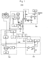
- In one possible arrangement, as shown in Figure 1(A), tuner video signals b, which are selected through a
switching section 1 in order to switch the tuner line video input, are supplied to alow pass filter 2. Thislow pass filter 2 is a component of a tuner synchronizingseparation section 100 which includes thelow pass filter 2, asynchronizing isolator 3, a horizontal automaticfrequency control section 4, ahorizontal oscillator 5, inverters 3A, A, A', and anAND gate 16. - The signals which are filtered through the
low pass filter 2 are simultaneously supplied to both the synchronizingisolator 3 and the horizontal automaticfrequency control section 4. The output of the horizontal automaticfrequency control section 4 is supplied to thehorizontal oscillator 5 in order to control the horizontal synchronizing signal generation, and the horizontal synchronizing signals which are generated through thehorizontal oscillator 5 are supplied to an input terminal of theAND gate 16. - The synchronizing signals which are isolated through the synchronizing
isolator 3 are supplied to another input terminal of theAND gate 16 where the signals of thehorizontal oscillator 5 are supplied through the other input terminal. - The output of the
AND gate 16 is supplied to the base of a transistor Q2 of a modulator video input muter (suppression)circuit 200 which includes transistors Q2-Q5, and which is for preventing tuner/line interference. The output of theAND gate 16 is supplied through the inverter A to the input terminal of the inverter A′, and the output of the inverter A′ is supplied to both achroma drive 8 and alow pass filter 6 of a Y/C (brightness/colour)separation section 300. - The
section 300 includes thelow pass filter 6, thechroma drive 8 and a synchronizingisolator 7, and is connected to the tuner video b. - The output of the
low pass filter 6, which removes the colour components of the video signals inputted to the Y/C separation section 300, is supplied through the synchronizingisolator 7 to adelay section 500, the synchronizingseparation section 7 being for extracting B.G.P. (burst gate pulse), and thedelay section 500 consists of inverters I1 and I2 and a schmidt trigger ST. - The output of a
discriminating section 400 which includes a B.G.P. delaying detectingsection 11, aburst gate 12, an OP amplifier OP1 and abuffer 13 is supplied to the PAL/MESECAM detection section 10. - Further, the output of the
delay section 500 is also supplied to the input terminal of the B.G.P. delaying detectingsection 11, while the output of the B.G.P. delaying detectingsection 11 is supplied to theburst gate 12. - The output signals of the
chroma drive section 8, which is for extracting the colour signals from the synchronizing signals supplied to the Y/C separation section 300, are supplied to theburst gate 12. The output of theburst gate 12 is supplied to the OP amplifier OP1 which carries out a comparison with the reference voltage as determined by resistances R7,R8. - The output of the OP amplifier OP1 is supplied through the
buffer 13 to a PAL/MESECAM detecting section 10 of a broadcasting methoddiscriminating section 700 which includes aphase detecting section 18, a recognition signal (ID) detectingsection 9 and acolour killer 19 in addition to the PAL/MESECAM detecting section 10. - The output of the PAL/
MESECAM detecting section 10 is supplied to both the recognition (ID)signal detecting section 9 and thephase detecting section 18. The recognition signal andphase detecting sections colour killer 19, and the line video output 'a' which is selected by theswitching device 1 is also supplied to both thelow pass filter 6 and thechroma drive section 8 of the Y/C separation section 300. - The modulator video
input muter circuit 200 receives through its base the output of theAND gate 16 of the tuner synchronizingseparation section 100, and the emitter of the transistor Q2 of thesection 200 is grounded. The collector of the transistor Q2 is connected to both the emitter of the transistor Q3 and the resistance R9 where the power source Vcc is supplied. - The base of the transistor Q3 is connected to the collector of the transistor Q4 which is grounded through its emitter and receives through its base the tuner high signals from a microcomputer. The collector of the transistor Q3 is connected to the base of the transistor Q5 which is grounded through its emitter. The collector of the transistor Q5 is connected through a capacitor C4 to a video input terminal IN, and also connected ultimately to a
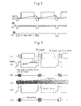
modulator 17. - The circuit constituted as above will now be described as to its operation referring to the timing charts of Figures 2 and 3.
- First, under the condition that the
mode switching device 1 of Figure 1 is selected, if a tuner video signal b is supplied to the tuner synchronizingseparation section 100, the colour or chroma signals C are removed by thelow pass filter 2, and only the signals (thewave pattern 1 of Figure 2) of the pure brightness or luminance component Y are supplied to both the synchronizingisolator 3 and the horizontal automaticfrequency control section 4. - Consequently, the synchronizing signals are isolated by the synchronizing
isolator 3, and the isolated signals pass through theinverter 3a with the result that the signals take thewave pattern 4 of Figure 2, and that they are supplied to one of the input terminals B of theAND gate 16. - Further, a saw tooth wave (
wave pattern 3 of Figure 2) is generated by the frequency (15·62 KHz) of the horizontal automaticfrequency control section 4, and therefore, the horizontal synchronizing signals generated from the horizontal synchronizingoscillator 5 are continuously triggered in such a manner that they exactly correspond to 64 microseconds. Then these signals are supplied to the other input terminal A of theAND gate 16 in the form of thewave pattern 2 of Figure 2. - The
AND gate 16 compares the two inputs A,B, and if the two inputs A,B are in a high state (that is, if it is the normal state in which video signals are received under the actual tuner mode), a high state output is produced and supplied to the base of the transistor Q2, so that transistor Q2 is turned on. Consequently, the potential of the collector of the transistor Q2 goes low and this low state is supplied to the emitter of the transistor Q3. - The transistor Q4 which receives a high signal from the micom is turned on in its collector and emitter so as for the collector of the transistor Q4 to have a low state before being supplied to the base of the power source driven transistor Q3.
- However, the transistor Q3 is turned off because of the low state of the emitter, and therefore, a low potential is supplied to the base of the transistor Q5 which is used in muting the inputted video signals of the
final modulator 17. - Consequently, the transistor Q5 is also turned off, so that video signals should be output through the
modulator 17 in a normal manner. Further, the high output of theAND gate 16 sequentially passes through the inverters A,A′, and therefore, muting is not carried out for the input video signals of the Y/C isolating section 300, with the result that the video signals are inputted into the Y/C isolating section 300 in a normal manner. - Consequently, only pure brightness signals Y having the
wave pattern 1 of Figure 2 are extracted by thelow pass filter 6, and then the extracted signals are supplied to the synchronizingisolator 7 where the signals are synchronized-isolated (BGP). The synchronizing signals (B.G.P) which are isolated by the synchronizingisolator 7 are sufficiently delayed by the synchronizingdelaying section 500, and then the signals are supplied to the B.G.P. delay detectingsection 11 of thediscriminating section 400 in the form of thewave pattern 2 of Figure 3. Then, a colour signal C having the form of thewave pattern 1 of Figure 3 is supplied to theburst gate 12 of thediscriminating section 400 by thechroma drive 8 of the Y/C isolating section 300, and consequently, colour burst and recognition signal gate portions are detected in the form of thewave pattern 3 of Figure 3 in theburst gate 12 by the BGP signals which are output from the BGP delaying detecting section 11 (PAL signals do not have frequency deviations, but MESECAM signals do). - Then, after going through the general procedures, (i.e. F-V conversion; in the case of PAL mode, there is no frequency deviation and no voltage difference, while, in the case of MESECAM mode, there are frequency deviations along with voltage differences), the signals are supplied to the OP amplifier OP1 where the signals are compared with the reference voltages of the supply resistances R7,R8.
- In the case of PAL, there is no voltage difference, and therefore, a low output OV is output, while, in the case of MESECAM, there are voltage differences, and therefore, high signals (4-5V) are output.
- Then the signals are supplied through the
output buffer 13 of the OP amplifier OP1 to the PAL/MESECAM detecting section 10 of a broadcasting methoddiscriminating section 700, and the PAL/MESECAM detecting section 10 is controlled by the output of the OP amplifier OP1 which is output through the buffer 13 (the output being low in the case of PAL, and the output being high in the case of MESECAM). The signals are detected by thephase detecting section 18 in the case of PAL signals, and by the recognitionsignal detecting section 9 in the case of MESECAM signals. Then, the requirement for colour killing is decided in the conventional manner by thecolour killer 19, and the colour signals are output after undergoing conventional processes and after being Y/C-mixed. The synchronising signals of thesynchronising isolator 3 of the Y/C isolating section 300 may include just the synchronising signals or, alternatively, both the synchronising signals and the BGP signals (refer to thewave pattern 2 of Figure 3), depending on the type of IC. Here, the description is given based on the assumption that both the synchronising signals and the BGP signals are simultaneously obtained. - If the two inputs A,B of the
AND gate 16 are different from each other (in the form of high, low or low, high), or if both of the inputs are low, the output of theAND gate 16 is shifted to a low state, with the result that the transistor Q2 of themuting circuit 200 is turned off, and that the transistors Q3, Q4,Q5 are turned on. - Consequently, the input video signals of the
modulator 17 are muted, and the output of theAND gate 16 is shifted to a low state after passing through the inverters A,A′, with the result that the video signals which are supplied to the Y/C isolating section 300 are also muted. - In the case where a line video 'a' is formed by the
mode switching device 1, the line video is also subjected to the extraction of the brightness signals Y by thelow pass filter 6 as in the case of the tuner video input. - Then synchronising (B.G.P) isolation is carried out by the
synchronising isolator 7, and then a delay is introduced by thedelay section 500 before being supplied to thediscriminating section 400. - Meanwhile, the line video colour signals are supplied to the
discriminating section 400 by thechroma driver section 8 after going through the general processes, and thediscriminating section 400 is operated in the same manner as when processing the tuner video signals. Thus the output of thesection 400 is supplied to the Y/C isolating section 300 which outputs it in the form of video signals. - The B.G.P signals will be described as a supplemental matter. That is, the B.G.P signals are needed for the following reason.
- If a signal having the form of the
wave pattern 1 of Figure 3 is input, then colour burst (PAL method) and recognition (ID) pulse (SECAM & MESECAM) will appear, and then a colour signal (chroma signal) having the form of thewave pattern 1 of Figure 3 is input. However, it is difficult to control all the colour signals, and therefore, the B.G.P signals are used in order to gate only the colour burst and recognition (ID) pulses and to discriminate between them. - However, when a VCR is used (regenerated) without tuner or line video signals, if the B.G.P signals are supplied to the
discriminating section 400 slightly in advance owing to the nature of the processing of the chroma signals, then the noise component of thewave pattern 4 of Figure 3 is gated to produce thewave pattern 6 owing to the wave pattern 5 (the wave pattern caused by the B.G.P delaying detecting section 11). - Consequently, the
discriminating section 400 carries out discriminating errors, and therefore, thecolour killer 19 has to be operated until the B.G.P and colour signals are normally operated, or delay or distortion of colours will appear. - That is, according to the circuit described above, if a synchronising signal is output in order to prevent interference to the tuner line under the tuner mode, there is present only a tuner circuit for preventing mode (line/tuner) interference and for carrying out video suppression. Therefore, in the case where a VCR is used during a non-signal or blanking period (without tuner/line video), the time period for processing the colour signals and supplying them to the discriminating section is longer than the time period for separating the synchronising signals (B.G.P.) and supplying them to the discriminating section to carry out gatings. Therefore, during tape loading, high pass noises are transferred from the
chroma drive section 8 to the detecting terminal with the result that they are input earlier than the colour signals. This results in the noise being erroneously recognised as a colour signal by the B.G.P. signal (performing the gating), thereby causing discrimination errors, and ultimately delaying the colour signals, and suppressing the colours. - To repeat, if there is no received synchronising signal, a synchronising signal (or a high signal) is output from the internal circuit in order to carry out video suppression through the inverters A,A'. However, when noise is produced which is similar in form to a synchronising signal, it is mistaken for a video signal, and therefore, in spite of the fact that there is no video signal, suppression cannot be perfectly carried out, with the result that the picture on the screen is distorted and so on.
- According to the invention there is provided a picture stabilising circuit for stabilising a picture signal particularly during non-signal input, comprising: a tuner synchronising separation section for receiving tuner video signals and for supplying an output signal indicating whether tuner video signals are being received; a video suppression circuit to be controlled by the output of the tuner synchronising separation section and for preventing tuner/line interferences; a Y/C separation section for receiving tuner/line video signals and carrying out Y/C separation; a discriminating section for receiving synchronising signals and the chroma signals separated by the Y/C separation section, detecting colour burst signals and recognition signals and comparing detected signals with a reference voltage to produce an output; and a broadcasting method discriminating section for discriminating and selecting the broadcasting method based on the output of the discriminating section,
wherein the stabilising circuit further comprises: a further suppression circuit for muting the chroma signals and the synchronising signals supplied to the discriminating section during non-signal input. - The present invention is intended to overcome the above described disadvantages of the conventional circuit by the provision of a picture regeneration stabilising circuit with dual suppression circuits.
- Preferably the further suppression circuit is controlled by the output of a synchronising signal isolator of the Y/C separation section, and the Y/C separation section is adapted to output synchronising signals (B.G.P.) in the presence of a line/tuner video signal input, and to output a high voltage in the absence of such input signals.
- In this way the noise which would otherwise be input to the discriminating section from the Y/C separation section is suppressed.
- The above object and other advantages of the present invention will become more apparent by describing in detail a preferred embodiment of the present invention with reference to the attached drawings in which:
- Figure 1(A) is a circuit diagram of a conventional picture regeneration stabilising circuit;
- Figure 1(B) is a variant thereof without a delay section;
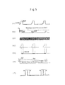
- Figure 2 is a timing chart for the tuner synchronising separation section of Figure 1;
- Figure 3 is a timing chart for the Y/C separation section of Figure 1;
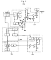
- Figure 4(A) is a circuit diagram of the picture regeneration stabilising circuit according to an embodiment of the present invention;
- Figure 4(B) is a variant thereof without a delay section; and
- Figure 5 is a timing chart for the circuit of Figure 4.
- The present invention provides an improvement of the conventional circuit in a manner described below. That is, the synchronising signals (B.G.P.) output from the synchronising
isolator 7 of the Y/C separation section 300 are supplied through integrating and dc flattening circuits d,e,f (respectively consisting of a resistance and a capacitor) and through a resistance R4 to the transistor Q1. The emitter of the transistor Q1 is grounded, and the collector of the transistor Q1 is connected through a resistance R5 to thedelay section 500, and to the output terminal of thechroma drive section 8 which is connected to theburst gate 12. - In describing the preferred embodiment of the present invention, only the modified portion constituted as above will be described as to its operations.
- That is, when video signals are input, the wave pattern 1 (SYNC+ B.G.P. signals) of Figure 5 is output from the synchronising
isolator 7. In this condition, the synchronising signals (B.G.P.) having the form of thewave pattern 1 of Figure 5 successively pass through the integrating circuit d consisting of resistance R1 and a capacitance C1, the integrating circuit e consisting of a resistance R2 and a capacitance C2, and the integrating circuit f consisting of a resistance R3 and a capacitance C3. Having done so, the signals take thewave pattern 2 of Figure 5, and are supplied to the base of the synchronising (B.G.P.) colour suppressing transistor Q1. - The signals supplied as described above (and taking the form of the
wave pattern 2 of Figure 5) will behave in such a manner that the synchronising (B.G.P.) signals and the chroma signals which have passed respectively through thedelay section 500 and thechroma drive section 8 will be supplied to the discriminatingsection 400 in the normal manner, because the supplied signal (wave pattern 2 of Figure 5) corresponds to (lies below) the active reference level of the transistor Q1, and consequently the transistor Q1 is turned off. - During a non-signal picture production (without any line/tuner video signals), a high voltage is output instead of a synchronising (B.G.P.) signal from the synchronising
isolator 7 of the Y/C separation section 300 (when there is no signal input, the power source voltage is output because of the inherent nature of the synchronising isolator). This high voltage is supplied to the base of the synchronising (B.G.P.) and colour muting transistor Q1 in the form of thewave pattern 6 of Figure 5, after passing through the integrating circuits d,e,f consisting respectively of resistance R1, capacitance C1, resistance R2, capacitance C2, resistance R3 and capacitance C3. - Consequently, because of the fact that the voltage supplied to the base of the transistor Q1 is higher than the active reference level of the transistor (Q1), the synchronising signals (B.G.P.) are suppressed in the form of the
wave pattern 4 of Figure 5, and consequently, the noise component having the form of thewave pattern 3 of Figure 5 and supplied from thechroma drive section 8 during the drum loading at the initial regeneration is not gated. - Therefore, noise components which are extremely weak like the
wave pattern 5 of Figure 5 are input to theburst gate 12. - In the case of an IC having no B.G.P. signals, the synchronising signals are delayed up to the colour burst and ID pulse positions, so that erroneous outputs of the discriminating section may be prevented, thereby making it possible to discriminate between PAL, MESECAM and SECAM. (Refer to the dotted synchronisation pulses, a′, of the
wave pattern 7 of Figure 5). That is, according to embodiments of the present invention, during non-signal input or blanking periods, the high voltage output from the synchronising isolator is utilized in order to drive the suppression transistor Q1, so that the noise which would otherwise be input into theburst gate 12 is eliminated, thereby stabilising the regenerated picture.
Claims (7)
- A picture stabilising circuit for receiving tuner/line video signals and for stabilising a picture signal particularly during non-signal input, comprising:a tuner synchronising separation section (100) for receiving tuner video signals (b), and for supplying an output signal indicating whether tuner video signals are being received;a video suppression circuit (200) to be controlled by the output of the tuner synchronising separation section (100) and for preventing tuner/line interferences;a Y/C separation section (300) for receiving tuner/line video signals and carrying out Y/C separation;a discriminating section (400) for receiving synchronising signals (B.G.P.) and the chroma signals separated by the Y/C separation section (300), detecting colour burst signals and recognition signals and comparing detected signals with a reference voltage to produce an output; anda broadcasting method discriminating section (700) for discriminating and selecting the broadcasting method based on the output of the discriminating section (400), wherein the stabilising circuit further comprises:
a further suppression circuit (600) for muting the chroma signals and the synchronising signals (B.G.P.) supplied to the discriminating section (400) during non-signal input. - A picture stabilising circuit as claimed in claim 1, in which the further suppression circuit (600) is controlled by the output of a synchronising signal isolator (7) of the Y/C separation section (300), and
the Y/C separation section (300) is adapted to output synchronising signals (B.G.P.) in the presence of a line/tuner video signal input, and to output a high voltage in the absence of such input signals. - A picture stabilising circuit as claimed in claim 2, wherein the further suppression circuit (600) comprises:an integrating circuit (d,e,f) for carrying out integration after receipt of the output of the said synchronising isolator (7) of the Y/C separation section (300), anda colour suppressing transistor (Q1) controlled by the signal integrated by the integrating circuit (d,e,f) for blocking the synchronisation pulses (B.G.P.) and the colour signals otherwise supplied to the discriminating section (400) during a non-signal or blanking period.
- The picture regeneration stabilising circuit as claimed in claim 3, in which the integration circuit consists of three integrating and dc-levelling circuits (d,e,f) arranged in series, each integrating and dc-levelling circuit (d,e,f) consisting of a resistor and a capacitor connected between the output of this resistor and earth.
- A picture regeneration stabilising circuit as claimed in claim 3 or 4, in which the colour suppressing transistor (Q1) has its collector connected via a resistor (R5) to form an output and provide a signal to the discriminating section (400) and its emitter connected to earth.
- A picture regeneration stabilising circuit according to any preceding claim and further comprising a delay line (500) through which the chroma and synchronising signals (B.G.P.) are supplied from the Y/C separation section to the discriminating section (400).
- A picture regeneration stabilising circuit according to any preceding claim, in which the discriminating section includes an output amplifier (13, OP1).
Applications Claiming Priority (2)
| Application Number | Priority Date | Filing Date | Title |
|---|---|---|---|
| KR237390 | 1990-02-28 | ||
| KR900002373 | 1990-02-28 |
Publications (3)
| Publication Number | Publication Date |
|---|---|
| EP0444925A2 EP0444925A2 (en) | 1991-09-04 |
| EP0444925A3 EP0444925A3 (en) | 1993-05-19 |
| EP0444925B1 true EP0444925B1 (en) | 1997-02-05 |
Family
ID=19296401
Family Applications (1)
| Application Number | Title | Priority Date | Filing Date |
|---|---|---|---|
| EP19910301634 Expired - Lifetime EP0444925B1 (en) | 1990-02-28 | 1991-02-28 | Picture stabilising circuit |
Country Status (1)
| Country | Link |
|---|---|
| EP (1) | EP0444925B1 (en) |
Family Cites Families (2)
| Publication number | Priority date | Publication date | Assignee | Title |
|---|---|---|---|---|
| FR2428362A1 (en) * | 1978-06-09 | 1980-01-04 | Thomson Csf | CHROMINANCE INFORMATION DECODING CIRCUIT, IN THE SECAM TELEVISION SYSTEM, AND TELEVISION RECEIVER INCLUDING SUCH A CIRCUIT |
| JPS62227291A (en) * | 1986-03-29 | 1987-10-06 | Toshiba Corp | Automatic color saturation controller |
-
1991
- 1991-02-28 EP EP19910301634 patent/EP0444925B1/en not_active Expired - Lifetime
Also Published As
| Publication number | Publication date |
|---|---|
| EP0444925A2 (en) | 1991-09-04 |
| EP0444925A3 (en) | 1993-05-19 |
Similar Documents
| Publication | Publication Date | Title |
|---|---|---|
| CA1252880A (en) | Multi-system television receiver | |
| US7805056B2 (en) | Methods and apparatus for providing cycles of normal and non normal phase in a color burst signal | |
| EP0084241B1 (en) | Signal processing device and method for video tape recording | |
| DK143728B (en) | LOADED SYNCHRONIZATION CIRCUIT FOR TELEVISION RECEIVERS | |
| JPH0566076B2 (en) | ||
| EP0173439B1 (en) | Luminance/chrominance separator | |
| EP0444925B1 (en) | Picture stabilising circuit | |
| EP0342634A2 (en) | Circuitry for and method of generating vertical drive pulse in video signal receiver | |
| JP3092938B2 (en) | Digital synchronization circuit for image display | |
| US5815213A (en) | Video signal synchronization extraction device | |
| US7777813B2 (en) | Color burst automatic detection device | |
| JP2619524B2 (en) | Ghost detection reference signal extraction circuit | |
| KR900000126B1 (en) | Multi-system television receiver | |
| KR910005705Y1 (en) | PAL / SECAM automatic color signal cancellation circuit | |
| KR940011032B1 (en) | Automatic tuning device | |
| US7432918B2 (en) | Video signal processing circuit | |
| JPS5825779A (en) | Multi-format color television receiver | |
| CA1262281A (en) | Multi-system television receiver | |
| JPH0723304A (en) | Video signal selection circuit signal detection circuit | |
| JP3456712B2 (en) | Composite video signal detection circuit | |
| JPS628628Y2 (en) | ||
| US5122867A (en) | Video signal processing circuit having a band pass filter following a delay circuit in a comb filter arrangement | |
| KR910004904Y1 (en) | Point noise elimination circuit by correlation detection | |
| SU1125782A1 (en) | Brightness signal channel for secam colour television receiver | |
| KR0131601Y1 (en) | Arm / Secam Method Discrimination Circuit Using 2 Horizontal Cycle Delays |
Legal Events
| Date | Code | Title | Description |
|---|---|---|---|
| PUAI | Public reference made under article 153(3) epc to a published international application that has entered the european phase |
Free format text: ORIGINAL CODE: 0009012 |
|
| AK | Designated contracting states |
Kind code of ref document: A2 Designated state(s): DE FR GB |
|
| PUAL | Search report despatched |
Free format text: ORIGINAL CODE: 0009013 |
|
| AK | Designated contracting states |
Kind code of ref document: A3 Designated state(s): DE FR GB |
|
| 17P | Request for examination filed |
Effective date: 19930908 |
|
| 17Q | First examination report despatched |
Effective date: 19950818 |
|
| GRAG | Despatch of communication of intention to grant |
Free format text: ORIGINAL CODE: EPIDOS AGRA |
|
| GRAH | Despatch of communication of intention to grant a patent |
Free format text: ORIGINAL CODE: EPIDOS IGRA |
|
| GRAH | Despatch of communication of intention to grant a patent |
Free format text: ORIGINAL CODE: EPIDOS IGRA |
|
| GRAA | (expected) grant |
Free format text: ORIGINAL CODE: 0009210 |
|
| AK | Designated contracting states |
Kind code of ref document: B1 Designated state(s): DE FR GB |
|
| REF | Corresponds to: |
Ref document number: 69124535 Country of ref document: DE Date of ref document: 19970320 |
|
| ET | Fr: translation filed | ||
| PLBE | No opposition filed within time limit |
Free format text: ORIGINAL CODE: 0009261 |
|
| STAA | Information on the status of an ep patent application or granted ep patent |
Free format text: STATUS: NO OPPOSITION FILED WITHIN TIME LIMIT |
|
| 26N | No opposition filed | ||
| REG | Reference to a national code |
Ref country code: GB Ref legal event code: IF02 |
|
| PGFP | Annual fee paid to national office [announced via postgrant information from national office to epo] |
Ref country code: FR Payment date: 20100223 Year of fee payment: 20 |
|
| PGFP | Annual fee paid to national office [announced via postgrant information from national office to epo] |
Ref country code: GB Payment date: 20100224 Year of fee payment: 20 Ref country code: DE Payment date: 20100312 Year of fee payment: 20 |
|
| REG | Reference to a national code |
Ref country code: DE Ref legal event code: R071 Ref document number: 69124535 Country of ref document: DE |
|
| REG | Reference to a national code |
Ref country code: GB Ref legal event code: PE20 Expiry date: 20110227 |
|
| PG25 | Lapsed in a contracting state [announced via postgrant information from national office to epo] |
Ref country code: GB Free format text: LAPSE BECAUSE OF EXPIRATION OF PROTECTION Effective date: 20110227 |
|
| PG25 | Lapsed in a contracting state [announced via postgrant information from national office to epo] |
Ref country code: DE Free format text: LAPSE BECAUSE OF EXPIRATION OF PROTECTION Effective date: 20110228 |