EP0444622A2 - Circuit breaker with detachable tripping tester - Google Patents
Circuit breaker with detachable tripping tester Download PDFInfo
- Publication number
- EP0444622A2 EP0444622A2 EP91102837A EP91102837A EP0444622A2 EP 0444622 A2 EP0444622 A2 EP 0444622A2 EP 91102837 A EP91102837 A EP 91102837A EP 91102837 A EP91102837 A EP 91102837A EP 0444622 A2 EP0444622 A2 EP 0444622A2
- Authority
- EP
- European Patent Office
- Prior art keywords
- tripping
- terminal
- circuit
- switch
- power source
- Prior art date
- Legal status (The legal status is an assumption and is not a legal conclusion. Google has not performed a legal analysis and makes no representation as to the accuracy of the status listed.)
- Withdrawn
Links
- 238000006243 chemical reaction Methods 0.000 description 4
- 238000010586 diagram Methods 0.000 description 4
- 239000007787 solid Substances 0.000 description 3
- 238000001514 detection method Methods 0.000 description 2
- 238000004804 winding Methods 0.000 description 2
- 238000010276 construction Methods 0.000 description 1
- 230000009466 transformation Effects 0.000 description 1
Images


Classifications
-
- H—ELECTRICITY
- H02—GENERATION; CONVERSION OR DISTRIBUTION OF ELECTRIC POWER
- H02H—EMERGENCY PROTECTIVE CIRCUIT ARRANGEMENTS
- H02H3/00—Emergency protective circuit arrangements for automatic disconnection directly responsive to an undesired change from normal electric working condition with or without subsequent reconnection ; integrated protection
- H02H3/02—Details
- H02H3/04—Details with warning or supervision in addition to disconnection, e.g. for indicating that protective apparatus has functioned
- H02H3/044—Checking correct functioning of protective arrangements, e.g. by simulating a fault
-
- H—ELECTRICITY
- H01—ELECTRIC ELEMENTS
- H01H—ELECTRIC SWITCHES; RELAYS; SELECTORS; EMERGENCY PROTECTIVE DEVICES
- H01H69/00—Apparatus or processes for the manufacture of emergency protective devices
-
- H—ELECTRICITY
- H04—ELECTRIC COMMUNICATION TECHNIQUE
- H04M—TELEPHONIC COMMUNICATION
- H04M3/00—Automatic or semi-automatic exchanges
- H04M3/22—Arrangements for supervision, monitoring or testing
-
- H—ELECTRICITY
- H04—ELECTRIC COMMUNICATION TECHNIQUE
- H04Q—SELECTING
- H04Q1/00—Details of selecting apparatus or arrangements
- H04Q1/18—Electrical details
- H04Q1/20—Testing circuits or apparatus; Circuits or apparatus for detecting, indicating, or signalling faults or troubles
Definitions
- the present invention relates to a circuit breaker having tripping test function, and especially relates to a circuit breaker having a detachable tripping tester to be used for not only a tripping tester but also a remote controller for manually tripping the circuit breaker.
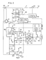
- FIG.3 is a circuit diagram showing the conventional circuit breaker having tripping test function.
- a connector 11 for testing operation has terminals 11a, 11b, 11c and 11d.
- the terminal 11a is connected to a negative terminal 5d of an electric power circuit 500.
- the terminal 11b is connected to the anode of a diode 12 which is for preventing reverse current to the terminals.
- the cathode of the diode 12 is connected to a positive terminal 30a of a rectifying circuit 30.
- the terminal 11c is connected to a first test signal generating circuit 13 and the terminal 11d is connected to a second test signal generating circuit 14.
- Terminals 15a, 15b, 15c and 15d are disconnectably connected to the terminals 11a, 11b, 11c and 11d, respectively.
- the terminal 15a is connected to the negative electrode of a D.C. power source 16.
- Other terminals 15b, 15c and 15d are respectively connected to switches 17a, 17b and 17c.
- the switches 17a, 17b and 17c are connected to the positive electrode of the D.C. power source 16.
- terminals 15a, 15b, 15c and 15d are connected to the contacts 11a, 11b, 11c and 11d of the connector 11, respectively.
- a predetermined voltage for example, 24V is applied to the electric power circuit 500 from the outer D.C. power source 16, and a direct current (D.C.) flows on the electric power circuit 500.
- D.C. direct current
- a switch 18 is turned to a first D.C. power source 19 by the output of the first test signal generating circuit 13.
- the voltage from the first D.C. power source 19 is applied to the positive input terminal of a differential amplifier 60 as an input signal and the output signal of the differential amplifier 60 is applied to a time delay circuit 70.
- an instant time tripping circuit 230 issues an output in the instant time tripping region as an output of the time delay circuit 70.
- a switch 22 is turned to a second D.C. power source 20 by the output of the second test signal generating circuit 14.
- the voltage from the second D.C. power source 20 is applied to the positive input terminal of a differential amplifier 61 as an input signal.
- the output signal of the differential amplifier 61 is applied to the time delay circuit 70.
- the long time tripping circuit 170 issues an output of a long time tripping region as an output of the time delay circuit 70.
- the conventional testing of the instant time tripping characteristic and the long time tripping characteristic in the state of connection of the circuit breaker actually to the power line is executed by following sequential steps of: connecting the terminals 15a, 15b, 15c and 15d to the contacts 11a, 11b, 11c and 11d of the connector 11 respectively for testing operation and turning on the switch 17; supplying the voltage of the D.C. power source 16 to the electric power circuit 500; closing the switch 17b or 17c; turning the switch 18 or 22 to be connected to the D.C. power source 19 or 20 by the output of the first or second test signal generating circuit 13 or 14; and applying the output voltage of the first or second D.C. power source 19 or 20 as a quasi input signal to the differential amplifier 60 or 61.
- a solid state circuit is used as a control circuit of the circuit breaker and it is known that the solid state circuit is reliable. Accordingly, when the solid state circuit is adopted as a control circuit of the conventional circuit shown in FIG.3, testing relatively often is necessary only for mechanical operation of the tripping.
- the conventional circuit breaker having tripping test function comprises the circuit testing function performed by configuration of the test signal generating circuits 13 and 14, the D.C. power source 19 and 20 and the switches 18 and 22 for testing an instant time tripping operation and a long time or a short time tripping operation. Therefore, the complexity and the expensiveness of the control circuit of the conventional circuit breaker shown in FIG.3 become its disadvantage. Furthermore, the disconnectable unit consisting of the D.C. power source 16, the switches 17a--17c and the terminals 15a--15d are exclusively for the circuit of FIG.3, and the unit can not be used in another circuit breaker having different constitution from the circuit shown in FIG.3.
- Purpose of the present invention is to provide an improved circuit breaker with detachable tripping tester, wherein the tripping tester has the simplified constitution and is compatible in another circuit breaker having different constitution for tripping test.
- a circuit breaker with detachable tripping tester in accordance with the present invention comprises: first and second terminals provided on a surface of a housing of the circuit breaker, the first terminal being connected to a negative terminal of an electric power source of the circuit breaker, the second terminal being connected to the anode of a diode and the cathode of the diode being connected to a positive terminal of the electric power source; a series connection of a tripping coil and a first switch connected between the negative terminal and the positive terminal of the electric power source, an actuator of the tripping coil being linked to a tripping mechanism of the circuit breaker for driving the tripping mechanism when the switch is turned on; quasi over-current signal generating means connected between the second terminal and the negative terminal of the electric power source for generating a quasi over-current signal for turning on the switch when a predetermined D.C.
- detachable tripping tester having a D.C. power source, a second switch and third and fourth terminals, the third terminal being connected to a negative terminal of the D.C. power source and to be connected to the first terminal, the fourth terminal being connected to a terminal of the second switch and to be connected to the second terminal, and the other terminal of the switch being connected to a positive terminal of the D.C. power source.
- the way of tripping test by using the apparatus in accordance with the present invention is as follows.
- the third and fourth terminals of the detachable tripping tester are connected to the first and second terminals of the circuit breaker, respectively.
- a predetermined D.C. power is applied between the negative and positive terminals of the electric power source of the circuit breaker and the quasi over-current signal generating means (circuit).
- the quasi over-current generating means turns on the first switch and the tripping coil is excited by the D.C. power, since the series connection of the tripping coil and the first switch is connected to the electric power source of the circuit breaker.
- the tripping mechanism is driven and a switch on an electric power line is disconnected.
- FIG.1 is a perspective view showing a circuit breaker with detachable tripping tester in accordance with the present invention.
- FIG.2 is a circuit diagram of the circuit breaker with detachable tripping tester in accordance with the present invention.
- FIG.3 is the circuit diagram of the conventional circuit breaker having tripping test function.
- FIG.1 is a perspective view showing an external appearance of a part of the circuit breaker with detachable tripping tester in accordance with the present invention.
- FIG.2 is a circuit diagram of the circuit breaker with detachable tripping tester in accordance with the present invention. In this embodiment, only a single phase of the power line and a circuit breaker of a single phase are shown for making the description simple, but the actual system has three power lines and three circuit breakers of the same constitution.
- an detachable tripping tester 25 comprises a switch 17 such as an push button switch, an electric power source 16 such as a battery and a connector plug 15 including female terminals (third and fourth terminals) 15a and 15b.
- the switch 17, the electric power source 16 and the terminals 15a and 15b are electrically inter-connected by cables 18.
- An over-current tripping relay 26 is fixed on a front face 35a of a housing 35 of a circuit breaker or a switch box.
- Male terminals (first and second terminals) 11a and 11b of a connector receptacle 11 are provided on a front face 26a of the relay 26.
- the connector 15 is to be coupled to the connector 11.
- the female terminals 15a and 15b are electrically connected to the male terminals 11a and 11b, respectively.
- a terminal on electric power side 101 is to be connected to an A.C. electric power source (not shown); and a load break contact 201 is connected to the terminal on the electric power side 101.
- the A.C. power line 1 is connected between the load break contact 201 and a terminal on load side 301.
- a current transformer 21 is provided on the A.C. power line 1 at the section between the terminal 101 on electric power side and the terminal 301 on the load side.
- a full-wave rectifying circuit 30 is connected to secondary output terminals of the current transformer 21 for changing an alternating current flowing on secondary winding of the current transformer 21 into a unidirectional current.
- the full-wave rectifying circuit 30 consists of known two sets of series connection of diodes.
- An electric power circuit 500 for outputting a D.C. constant voltage is connected to a positive output terminal of the rectifying circuit 30.
- the electric power circuit 500 has a positive terminal 5a, a reference voltage output terminal 5b, a grounded middle output terminal 5c and a negative output terminal 5
- the negative terminal 5d of the electric power circuit 500 is connected to a terminal of a resistor 40 for current detection.
- the other terminal of the resistor 40 is connected to a terminal of another resistor 41 for current detection.
- the other terminal of the resistor 41 is connected to the negative terminal of the rectifying circuit 30.
- Each differential amplifier 60 or 61 consists of an operational amplifier 63 or 631 and four resistors 64, 65, 66 and 67 or 641, 651, 661 and 671. Electric power is supplied to the differential amplifiers 60 and 61 from the electric power circuit 500. Input terminals of the differential amplifiers 60 and 61 are connected to both terminals of the resistors 40 and 41, respectively. The differential amplifiers 60 and 61 convert the voltage drops by the resistors 40 and 41, respectively, to a voltage signal which is based on a middle voltage V0 of the electric power source 500.
- the relation of gains of the differential amplifiers 60 and 61 are selected such that the gain of the one nearer to the electric power circuit 500 is smaller than that of the other. In this embodiment, the relation is concluded that the gain of the differential amplifier 60 is smaller than that of the differential amplifier 61.
- a time delay circuit 70 comprises an instant time tripping circuit 230, a short time tripping circuit 220 and a long time tripping circuit 170. Respective output terminals of the instant time tripping circuit 230, the short time tripping circuit 220 and the long time tripping circuit 170 are connected commonly to an output terminal 70a of the time delay circuit 70.
- the instant time tripping circuit 230 is connected to the output terminal of the differential amplifier 60.
- a series connection of a peak value conversion circuit 210 and the short time tripping circuit 220 and another series connection of an effective value conversion circuit 211 and the long time tripping circuit 170 are connected parallel to the instant time tripping circuit 230.
- the instant time tripping circuit 230 outputs a trip signal at the time when the input signal thereto becomes above a first predetermined value.
- the short time tripping circuit 220 outputs a trip signal shortly after that the input of peak value from the peak value conversion circuit 210 becomes above a second predetermined value.
- the long time tripping circuit 170 outputs a trip signal after a predetermined long time period from that the input of effective value from the effective value conversion circuit 211 becomes above a third predetermined value.
- An electromagnetic tripping coil 80 is connected to a positive terminal of the rectifying circuit 30.
- a switching circuit 120 is connected between the other end of the electromagnetic tripping coil 80 and the negative terminal 5d of the electric power circuit 500.
- the electromagnetic tripping coil 80 is mechanically linked to the tripping mechanism 100 for opening the load break contact 201 provided on the A.C. power line 1 and is excited for driving the tripping mechanism 100 when the switching circuit 120 turns on.
- An insufficient-operation locking circuit 50 for locking the tripping operation when the voltage of the electric power circuit 500 is insufficient (i.e. below a predetermined voltage) has an output switch 54 which is connected between the switching circuit 120 and the time delay circuit 70.
- the connector 11 which is provided on the front face 26a of the relay 26 as shown in FIG.1 has the terminals 11a and 11b.
- the terminal 11a is connected to the negative terminal 5d of the electric power circuit 500.
- the terminal 11b is connected to the anode of a diode 12 which is for preventing reverse current to the terminal 11b.
- the cathode of the diode 12 is connected to the positive terminal 30a of the rectifying circuit 30.
- the terminals 15a and 15b of the connector 15 are detachably connected to the terminals 11a and 11b.
- the terminal 15a is connected to the negative electrode of the D.C. electric power source 16.
- the other terminal 15b is connected to the switch 17.
- the switch 17 is connected to the positive electrode of the D.C. electric power source 16.
- the connector plug 15 is coupled to the connector receptacle 11 and thereby the terminals 15a and 15b are respectively connected to the terminals 11a and 11b.
- a predetermined D.C. voltage for example, 24V is applied to the electric power circuit 500 from the D.C. power source 16, and a direct current (D.C.) flows on the electric power circuit 500.
- the predetermined D.C. voltage from the D.C. power source 16 is applied to the test signal generating circuit 13.
- the test signal generating circuit 13 outputs a test signal for turning on the switch 18.
- a predetermined D.C. voltage from the first D.C. power source 19 is applied to the positive input terminal of the differential amplifier 60 as an input signal and the output signal of the differential amplifier 60 is applied to the time delay circuit 70.
- the instant time tripping circuit 230 issues an instant trip signal as a quasi over-current signal of the time delay circuit 70 to make an instant trip of the tripping mechanism 100.
- the above-mentioned circuit breaker with detachable tripping tester in accordance with the present invention has another advantageous that the detachable tripping tester 25 can be used as a remote control device for manual tripping of the circuit breaker.
- the test signal generating circuit 13 makes the switch 18 turn on.
- the switch 18 turns on, the predetermined D.C. voltage from the D.C. power source 19 is superposed on the output voltage between the terminals of the register 40.
- the time delay circuit 70 outputs a signal for turning on the switching circuit 120 for exciting the tripping coil 80.
- the load break contact 201 is opened by remote controlling.
- a circuit breaker for breaking double or triple phases of A.C. power lines can be realized by comprising: plural current transformers for converting the currents flowing on the double or triple phases of A.C. power lines to output currents of secondary winding in proportion to predetermined ratio of current transformation; plural rectifying circuits for converting the alternating secondary output current of the current transformers to unidirectional currents; plural (two or three) sets of series connections of two resistors which are also connected to an electric power circuit whereon the output current of the rectifying circuits flow; and plural sets of differential amplifier, test signal generating circuit, switch and so on corresponding to respective resistors.
- the circuit breaker for plural phases of A.C. power lines has checking function of the tripping characteristics similar to the afore-mentioned embodiment.
- the detachable tripping tester 25 has the simplest constitution having only the switch 17 and the D.C. power source 16 such as a battery. Therefore, only one detachable tripping tester 25 can be used for testing the tripping mechanism of all the circuit breaker for all phases.
Abstract
Description
- The present invention relates to a circuit breaker having tripping test function, and especially relates to a circuit breaker having a detachable tripping tester to be used for not only a tripping tester but also a remote controller for manually tripping the circuit breaker.
- A conventional circuit breaker having tripping test function, for example. shown in the United States Patent 4,873,603 is described referring to FIG.3. FIG.3 is a circuit diagram showing the conventional circuit breaker having tripping test function.
- In FIG.3, a
connector 11 for testing operation hasterminals terminal 11a is connected to anegative terminal 5d of anelectric power circuit 500. Theterminal 11b is connected to the anode of adiode 12 which is for preventing reverse current to the terminals. And the cathode of thediode 12 is connected to apositive terminal 30a of a rectifyingcircuit 30. The terminal 11c is connected to a first testsignal generating circuit 13 and the terminal 11d is connected to a second test signal generating circuit 14. -
Terminals terminals terminal 15a is connected to the negative electrode of aD.C. power source 16.Other terminals 15b, 15c and 15d are respectively connected toswitches switches D.C. power source 16. - Tripping test operation of the above-mentioned conventional circuit breaker is described.
- At first, the
terminals contacts connector 11, respectively. - Under the condition that the
load break contact 201 is opened and any current does not flow on the A.C. power line 1, when the switch 17a is closed, a predetermined voltage, for example, 24V is applied to theelectric power circuit 500 from the outerD.C. power source 16, and a direct current (D.C.) flows on theelectric power circuit 500. - Under the above-mentioned condition, when the
switch 17b is closed, aswitch 18 is turned to a firstD.C. power source 19 by the output of the first testsignal generating circuit 13. The voltage from the firstD.C. power source 19 is applied to the positive input terminal of adifferential amplifier 60 as an input signal and the output signal of thedifferential amplifier 60 is applied to atime delay circuit 70. Hereupon, since the level of the output signal of thedifferential amplifier 60 is high, an instanttime tripping circuit 230 issues an output in the instant time tripping region as an output of thetime delay circuit 70. - On the contrary, when the
switch 17c is closed instead of theswitch 17b, aswitch 22 is turned to a secondD.C. power source 20 by the output of the second test signal generating circuit 14. The voltage from the secondD.C. power source 20 is applied to the positive input terminal of adifferential amplifier 61 as an input signal. And the output signal of thedifferential amplifier 61 is applied to thetime delay circuit 70. Hereupon, since the level of the output signal of thedifferential amplifier 61 is relatively lower than that of thedifferential amplifier 60, the longtime tripping circuit 170 issues an output of a long time tripping region as an output of thetime delay circuit 70. - As is obvious from the above-mentioned configuration, the conventional testing of the instant time tripping characteristic and the long time tripping characteristic in the state of connection of the circuit breaker actually to the power line is executed by following sequential steps of: connecting the
terminals contacts connector 11 respectively for testing operation and turning on theswitch 17; supplying the voltage of theD.C. power source 16 to theelectric power circuit 500; closing theswitch switch D.C. power source signal generating circuit 13 or 14; and applying the output voltage of the first or secondD.C. power source differential amplifier - Besides, a solid state circuit is used as a control circuit of the circuit breaker and it is known that the solid state circuit is reliable. Accordingly, when the solid state circuit is adopted as a control circuit of the conventional circuit shown in FIG.3, testing relatively often is necessary only for mechanical operation of the tripping.
- The conventional circuit breaker having tripping test function comprises the circuit testing function performed by configuration of the test
signal generating circuits 13 and 14, theD.C. power source switches D.C. power source 16, the switches 17a--17c and theterminals 15a--15d are exclusively for the circuit of FIG.3, and the unit can not be used in another circuit breaker having different constitution from the circuit shown in FIG.3. - Purpose of the present invention is to provide an improved circuit breaker with detachable tripping tester, wherein the tripping tester has the simplified constitution and is compatible in another circuit breaker having different constitution for tripping test.
- A circuit breaker with detachable tripping tester in accordance with the present invention comprises:
first and second terminals provided on a surface of a housing of the circuit breaker, the first terminal being connected to a negative terminal of an electric power source of the circuit breaker, the second terminal being connected to the anode of a diode and the cathode of the diode being connected to a positive terminal of the electric power source;
a series connection of a tripping coil and a first switch connected between the negative terminal and the positive terminal of the electric power source, an actuator of the tripping coil being linked to a tripping mechanism of the circuit breaker for driving the tripping mechanism when the switch is turned on;
quasi over-current signal generating means connected between the second terminal and the negative terminal of the electric power source for generating a quasi over-current signal for turning on the switch when a predetermined D.C. voltage is applied thereto; and
detachable tripping tester having a D.C. power source, a second switch and third and fourth terminals, the third terminal being connected to a negative terminal of the D.C. power source and to be connected to the first terminal, the fourth terminal being connected to a terminal of the second switch and to be connected to the second terminal, and the other terminal of the switch being connected to a positive terminal of the D.C. power source. - The way of tripping test by using the apparatus in accordance with the present invention is as follows. At first, the third and fourth terminals of the detachable tripping tester are connected to the first and second terminals of the circuit breaker, respectively. When the second switch of the detachable tripping tester is turned on, a predetermined D.C. power is applied between the negative and positive terminals of the electric power source of the circuit breaker and the quasi over-current signal generating means (circuit). The quasi over-current generating means turns on the first switch and the tripping coil is excited by the D.C. power, since the series connection of the tripping coil and the first switch is connected to the electric power source of the circuit breaker. When the tripping coil is excited, the tripping mechanism is driven and a switch on an electric power line is disconnected.
- FIG.1 is a perspective view showing a circuit breaker with detachable tripping tester in accordance with the present invention.
- FIG.2 is a circuit diagram of the circuit breaker with detachable tripping tester in accordance with the present invention.
- FIG.3 is the circuit diagram of the conventional circuit breaker having tripping test function.
- A preferred embodiment of a circuit breaker with detachable tripping tester in accordance with the present invention is described referring to FIGs.1 and 2. FIG.1 is a perspective view showing an external appearance of a part of the circuit breaker with detachable tripping tester in accordance with the present invention. FIG.2 is a circuit diagram of the circuit breaker with detachable tripping tester in accordance with the present invention. In this embodiment, only a single phase of the power line and a circuit breaker of a single phase are shown for making the description simple, but the actual system has three power lines and three circuit breakers of the same constitution.
- In FIG.1, an detachable tripping
tester 25 comprises aswitch 17 such as an push button switch, anelectric power source 16 such as a battery and aconnector plug 15 including female terminals (third and fourth terminals) 15a and 15b. Theswitch 17, theelectric power source 16 and theterminals cables 18. Anover-current tripping relay 26 is fixed on afront face 35a of ahousing 35 of a circuit breaker or a switch box. Male terminals (first and second terminals) 11a and 11b of aconnector receptacle 11 are provided on afront face 26a of therelay 26. Theconnector 15 is to be coupled to theconnector 11. And thefemale terminals male terminals - In FIG.2, a terminal on
electric power side 101 is to be connected to an A.C. electric power source (not shown); and aload break contact 201 is connected to the terminal on theelectric power side 101. The A.C. power line 1 is connected between theload break contact 201 and a terminal onload side 301. Acurrent transformer 21 is provided on the A.C. power line 1 at the section between the terminal 101 on electric power side and the terminal 301 on the load side. A full-wave rectifying circuit 30 is connected to secondary output terminals of thecurrent transformer 21 for changing an alternating current flowing on secondary winding of thecurrent transformer 21 into a unidirectional current. The full-wave rectifyingcircuit 30 consists of known two sets of series connection of diodes. Anelectric power circuit 500 for outputting a D.C. constant voltage is connected to a positive output terminal of the rectifyingcircuit 30. Theelectric power circuit 500 has apositive terminal 5a, a referencevoltage output terminal 5b, a grounded middle output terminal 5c and anegative output terminal 5d. - The negative terminal 5d of the
electric power circuit 500 is connected to a terminal of aresistor 40 for current detection. The other terminal of theresistor 40 is connected to a terminal of anotherresistor 41 for current detection. The other terminal of theresistor 41 is connected to the negative terminal of the rectifyingcircuit 30. - Each
differential amplifier operational amplifier resistors differential amplifiers electric power circuit 500. Input terminals of thedifferential amplifiers resistors differential amplifiers resistors electric power source 500. The relation of gains of thedifferential amplifiers electric power circuit 500 is smaller than that of the other. In this embodiment, the relation is concluded that the gain of thedifferential amplifier 60 is smaller than that of thedifferential amplifier 61. - A
time delay circuit 70 comprises an instanttime tripping circuit 230, a shorttime tripping circuit 220 and a longtime tripping circuit 170. Respective output terminals of the instanttime tripping circuit 230, the shorttime tripping circuit 220 and the longtime tripping circuit 170 are connected commonly to anoutput terminal 70a of thetime delay circuit 70. The instanttime tripping circuit 230 is connected to the output terminal of thedifferential amplifier 60. And a series connection of a peakvalue conversion circuit 210 and the shorttime tripping circuit 220 and another series connection of an effective value conversion circuit 211 and the longtime tripping circuit 170 are connected parallel to the instanttime tripping circuit 230. The instanttime tripping circuit 230 outputs a trip signal at the time when the input signal thereto becomes above a first predetermined value. The shorttime tripping circuit 220 outputs a trip signal shortly after that the input of peak value from the peakvalue conversion circuit 210 becomes above a second predetermined value. And the longtime tripping circuit 170 outputs a trip signal after a predetermined long time period from that the input of effective value from the effective value conversion circuit 211 becomes above a third predetermined value. - One end of an electromagnetic tripping
coil 80 is connected to a positive terminal of the rectifyingcircuit 30. A switchingcircuit 120 is connected between the other end of the electromagnetic trippingcoil 80 and the negative terminal 5d of theelectric power circuit 500. The electromagnetic trippingcoil 80 is mechanically linked to the trippingmechanism 100 for opening theload break contact 201 provided on the A.C. power line 1 and is excited for driving the trippingmechanism 100 when theswitching circuit 120 turns on. - An insufficient-
operation locking circuit 50 for locking the tripping operation when the voltage of theelectric power circuit 500 is insufficient (i.e. below a predetermined voltage) has anoutput switch 54 which is connected between the switchingcircuit 120 and thetime delay circuit 70. - The
connector 11 which is provided on thefront face 26a of therelay 26 as shown in FIG.1 has theterminals electric power circuit 500. The terminal 11b is connected to the anode of adiode 12 which is for preventing reverse current to the terminal 11b. And the cathode of thediode 12 is connected to thepositive terminal 30a of the rectifyingcircuit 30. - The
terminals connector 15 are detachably connected to theterminals electric power source 16. Theother terminal 15b is connected to theswitch 17. Theswitch 17 is connected to the positive electrode of the D.C.electric power source 16. - Tripping test operation of the above-mentioned circuit breaker with detachable tripping tester in accordance with the present invention is described.
- At first, the
connector plug 15 is coupled to theconnector receptacle 11 and thereby theterminals terminals - Under the condition that the
load break contact 201 is opened and any current does not flow on the A.C. power line 1, when theswitch 17 is closed, a predetermined D.C. voltage, for example, 24V is applied to theelectric power circuit 500 from theD.C. power source 16, and a direct current (D.C.) flows on theelectric power circuit 500. - At this time, the predetermined D.C. voltage from the
D.C. power source 16 is applied to the testsignal generating circuit 13. The testsignal generating circuit 13 outputs a test signal for turning on theswitch 18. When theswitch 18 is turned on, a predetermined D.C. voltage from the firstD.C. power source 19 is applied to the positive input terminal of thedifferential amplifier 60 as an input signal and the output signal of thedifferential amplifier 60 is applied to thetime delay circuit 70. Hereupon, since the level of the output signal of thedifferential amplifier 60 is high, the instanttime tripping circuit 230 issues an instant trip signal as a quasi over-current signal of thetime delay circuit 70 to make an instant trip of the trippingmechanism 100. - Furthermore, in the above-mentioned embodiment, under condition that the
load break contact 201 is closed and the A.C. power line 1 is electified, even when each of thecontact connector 11 happens to be short-circuited, unexpected accident which badly affects the instant time tripping characteristic or the long time tripping characteristic does not occur, because thediode 12 for preventing the reverse current is connected between thecontact 11b and the positive terminal of the rectifyingcircuit 30. - Still more, the above-mentioned circuit breaker with detachable tripping tester in accordance with the present invention has another advantageous that the detachable tripping
tester 25 can be used as a remote control device for manual tripping of the circuit breaker. Namely, under the normal condition that theload break contact 201 is closed and the A.C. power line 1 is electified to flow current thereon, when theswitch 17 is turned on, the testsignal generating circuit 13 makes theswitch 18 turn on. When theswitch 18 turns on, the predetermined D.C. voltage from theD.C. power source 19 is superposed on the output voltage between the terminals of theregister 40. And thetime delay circuit 70 outputs a signal for turning on theswitching circuit 120 for exciting the trippingcoil 80. Thereby, theload break contact 201 is opened by remote controlling. - The above-mentioned embodiment has been described as a circuit breaker for breaking single phase of A.C. power line for simplicity's sake. However, a circuit breaker for breaking double or triple phases of A.C. power lines can be realized by comprising: plural current transformers for converting the currents flowing on the double or triple phases of A.C. power lines to output currents of secondary winding in proportion to predetermined ratio of current transformation; plural rectifying circuits for converting the alternating secondary output current of the current transformers to unidirectional currents; plural (two or three) sets of series connections of two resistors which are also connected to an electric power circuit whereon the output current of the rectifying circuits flow; and plural sets of differential amplifier, test signal generating circuit, switch and so on corresponding to respective resistors. Thereby, the circuit breaker for plural phases of A.C. power lines has checking function of the tripping characteristics similar to the afore-mentioned embodiment.
- Hereupon, the detachable tripping
tester 25 has the simplest constitution having only theswitch 17 and theD.C. power source 16 such as a battery. Therefore, only one detachable trippingtester 25 can be used for testing the tripping mechanism of all the circuit breaker for all phases. - Although the invention has been described in its preferred form with a certain degree of particularity, it is understood that the present disclosure of the preferred form has been changed in the details of construction and the combination and arrangement of parts may be resorted to without departing from the spirit and the scope of the invention as hereinafter claimed.
Claims (3)
- A circuit breaker with detachable tripping tester comprising:
first and second terminals provided on a surface of a housing of said circuit breaker;
a series connection of a tripping coil and a first switch connected between said negative terminal and said positive terminal of said electric power source, an actuator of said tripping coil being linked to a tripping mechanism of said circuit breaker for driving said tripping mechanism when said switch is turned on;
quasi over-current signal generating means connected between said second terminal and said negative terminal of said electric power source for generating a quasi over-current signal for turning on said switch when a predetermined D.C. voltage is applied thereto; and
detachable tripping tester having a D.C. power source, a second switch and third and fourth terminals, said third terminal being connected to said first terminal, said fourth terminal being connected to said second terminal. - A circuit breaker with detachable tripping tester comprising:
first and second terminals provided on a surface of a housing of said circuit breaker, said first terminal being connected to a negative terminal of an electric power source of said circuit breaker, said second terminal being connected to the anode of a diode and the cathode of said diode being connected to a positive terminal of said electric power source;
a series connection of a tripping coil and a first switch connected between said negative terminal and said positive terminal of said electric power source, an actuator of said tripping coil being linked to a tripping mechanism of said circuit breaker for driving said tripping mechanism when said switch is turned on;
quasi over-current signal generating means connected between said second terminal and said negative terminal of said electric power source for generating a quasi over-current signal for turning on said switch when a predetermined D.C. voltage is applied thereto; and
detachable tripping tester having a D.C. power source, a second switch and third and fourth terminals, said third terminal being connected to a negative terminal of said D.C. power source and to be connected to said first terminal, said fourth terminal being connected to a terminal of said second switch and to be connected to said second terminal, and said other terminal of said switch being connected to a positive terminal of said D.C. power source. - A circuit breaker with detachable tripping tester in accordance with claim 1 or 2, wherein
said D.C. power source is a battery and said second switch is a push button switch.
Applications Claiming Priority (2)
| Application Number | Priority Date | Filing Date | Title |
|---|---|---|---|
| JP45586/90 | 1990-02-28 | ||
| JP2045586A JPH0766724B2 (en) | 1990-02-28 | 1990-02-28 | Circuit breaker |
Publications (2)
| Publication Number | Publication Date |
|---|---|
| EP0444622A2 true EP0444622A2 (en) | 1991-09-04 |
| EP0444622A3 EP0444622A3 (en) | 1992-07-29 |
Family
ID=12723453
Family Applications (1)
| Application Number | Title | Priority Date | Filing Date |
|---|---|---|---|
| EP19910102837 Withdrawn EP0444622A3 (en) | 1990-02-28 | 1991-02-26 | Circuit breaker with detachable tripping tester |
Country Status (5)
| Country | Link |
|---|---|
| US (1) | US5173833A (en) |
| EP (1) | EP0444622A3 (en) |
| JP (1) | JPH0766724B2 (en) |
| KR (1) | KR910016027A (en) |
| ZA (1) | ZA911386B (en) |
Cited By (3)
| Publication number | Priority date | Publication date | Assignee | Title |
|---|---|---|---|---|
| WO2001089052A1 (en) * | 2000-05-16 | 2001-11-22 | Siemens Aktiengesellschaft | Circuit breaker remote service system |
| GB2388977A (en) * | 2002-05-24 | 2003-11-26 | Fung Yip Electrical Mfg Ltd | A load overcurrent alarm device and a connector overheat alarm device |
| CN104638602A (en) * | 2015-03-03 | 2015-05-20 | 周云侠 | Alternating current power source power-off prompting device |
Families Citing this family (2)
| Publication number | Priority date | Publication date | Assignee | Title |
|---|---|---|---|---|
| US5446386A (en) * | 1993-02-26 | 1995-08-29 | General Electric Company | Molded case circuit breaker auxiliary power supply plug |
| IL140047A0 (en) * | 2000-03-27 | 2002-02-10 | Good Space Ltd | Vehicle related services system and methodology |
Citations (4)
| Publication number | Priority date | Publication date | Assignee | Title |
|---|---|---|---|---|
| FR2254137A1 (en) * | 1973-12-10 | 1975-07-04 | Simplex Appareils | Fault detector for overhead cables - detection circuit charges batteries from transformers if no fault occurs |
| US4105965A (en) * | 1977-07-14 | 1978-08-08 | General Electric Company | Static trip circuit breaker test set |
| US4803434A (en) * | 1988-03-18 | 1989-02-07 | Westinghouse Electric Corp. | Test device for circuit breakers having electronic trip units |
| EP0330148A2 (en) * | 1988-02-24 | 1989-08-30 | Mitsubishi Denki Kabushiki Kaisha | Circuit breaker |
Family Cites Families (2)
| Publication number | Priority date | Publication date | Assignee | Title |
|---|---|---|---|---|
| US3924160A (en) * | 1973-09-28 | 1975-12-02 | Westinghouse Electric Corp | Circuit breaker with detachably connected fault simulator |
| EP0235479B1 (en) * | 1986-01-10 | 1993-08-04 | Merlin Gerin | Static tripping unit with test circuit for electrical circuit interruptor |
-
1990
- 1990-02-28 JP JP2045586A patent/JPH0766724B2/en not_active Expired - Lifetime
- 1990-11-27 KR KR1019900019232A patent/KR910016027A/en not_active Application Discontinuation
-
1991
- 1991-02-25 US US07/659,684 patent/US5173833A/en not_active Expired - Fee Related
- 1991-02-26 EP EP19910102837 patent/EP0444622A3/en not_active Withdrawn
- 1991-02-26 ZA ZA911386A patent/ZA911386B/en unknown
Patent Citations (4)
| Publication number | Priority date | Publication date | Assignee | Title |
|---|---|---|---|---|
| FR2254137A1 (en) * | 1973-12-10 | 1975-07-04 | Simplex Appareils | Fault detector for overhead cables - detection circuit charges batteries from transformers if no fault occurs |
| US4105965A (en) * | 1977-07-14 | 1978-08-08 | General Electric Company | Static trip circuit breaker test set |
| EP0330148A2 (en) * | 1988-02-24 | 1989-08-30 | Mitsubishi Denki Kabushiki Kaisha | Circuit breaker |
| US4803434A (en) * | 1988-03-18 | 1989-02-07 | Westinghouse Electric Corp. | Test device for circuit breakers having electronic trip units |
Cited By (5)
| Publication number | Priority date | Publication date | Assignee | Title |
|---|---|---|---|---|
| WO2001089052A1 (en) * | 2000-05-16 | 2001-11-22 | Siemens Aktiengesellschaft | Circuit breaker remote service system |
| US6778650B1 (en) | 2000-05-16 | 2004-08-17 | Siemens Aktiengesellschaft | Circuit breaker remote service system |
| GB2388977A (en) * | 2002-05-24 | 2003-11-26 | Fung Yip Electrical Mfg Ltd | A load overcurrent alarm device and a connector overheat alarm device |
| SG105572A1 (en) * | 2002-05-24 | 2004-08-27 | Fung Yip Electrical Mfg Ltd | A load overcurrent alarm device and a connector overheat alarm device |
| CN104638602A (en) * | 2015-03-03 | 2015-05-20 | 周云侠 | Alternating current power source power-off prompting device |
Also Published As
| Publication number | Publication date |
|---|---|
| EP0444622A3 (en) | 1992-07-29 |
| JPH03250514A (en) | 1991-11-08 |
| ZA911386B (en) | 1992-10-28 |
| JPH0766724B2 (en) | 1995-07-19 |
| US5173833A (en) | 1992-12-22 |
| KR910016027A (en) | 1991-09-30 |
Similar Documents
| Publication | Publication Date | Title |
|---|---|---|
| US5757598A (en) | Ground fault circuit interrupter | |
| EP0289042B1 (en) | Circuit breaker | |
| GB2178255A (en) | Solid state power controller with leakage current shunt circuit | |
| US4713716A (en) | Detection device for contact fusion in an electromagnetic contactor | |
| US5173833A (en) | Circuit breaker with detachable tripping tester | |
| EP0330148B1 (en) | Circuit breaker | |
| CA1234905A (en) | 400 hz aircraft ground power supply | |
| US5267116A (en) | Electrical safety socket | |
| EP0302470B1 (en) | Circuit breaker including selectively operable long-time-delay tripping circuit | |
| EP0922322B1 (en) | Power back | |
| EP1386338B1 (en) | Electric pole for low-voltage power circuit breaker | |
| CA1331050C (en) | Electrical safety socket | |
| EP0542344A3 (en) | ||
| US3979599A (en) | Operatively interlocked electronic system | |
| EP1051786B1 (en) | Protective circuit breaking circuitry | |
| RU2752001C1 (en) | Automatic switch | |
| DE102017217267A1 (en) | Residual current circuit breaker and test circuit | |
| SU1737550A1 (en) | Reed relay-based high-voltage switching unit | |
| SU1120420A1 (en) | Three-phase switching device with short-circuit protection | |
| SU1725341A1 (en) | High-voltage stabilizer with changeable polarity of output voltage | |
| RU39755U1 (en) | INPUT PANEL | |
| SU1658268A1 (en) | Device for overload protection of high-voltage dc system | |
| SU1700686A1 (en) | Device for connection of three-phase load to mains through converter with protection against abnormal modes | |
| JPS6345769Y2 (en) | ||
| SU1826104A1 (en) | Device for current protection of sectionalizer busducts |
Legal Events
| Date | Code | Title | Description |
|---|---|---|---|
| PUAI | Public reference made under article 153(3) epc to a published international application that has entered the european phase |
Free format text: ORIGINAL CODE: 0009012 |
|
| AK | Designated contracting states |
Kind code of ref document: A2 Designated state(s): CH DE FR GB IT LI |
|
| PUAL | Search report despatched |
Free format text: ORIGINAL CODE: 0009013 |
|
| AK | Designated contracting states |
Kind code of ref document: A3 Designated state(s): CH DE FR GB IT LI |
|
| 17P | Request for examination filed |
Effective date: 19920630 |
|
| 17Q | First examination report despatched |
Effective date: 19941026 |
|
| STAA | Information on the status of an ep patent application or granted ep patent |
Free format text: STATUS: THE APPLICATION IS DEEMED TO BE WITHDRAWN |
|
| 18D | Application deemed to be withdrawn |
Effective date: 19951019 |