EP0443660B1 - Magnetoresistor - Google Patents
Magnetoresistor Download PDFInfo
- Publication number
- EP0443660B1 EP0443660B1 EP91200268A EP91200268A EP0443660B1 EP 0443660 B1 EP0443660 B1 EP 0443660B1 EP 91200268 A EP91200268 A EP 91200268A EP 91200268 A EP91200268 A EP 91200268A EP 0443660 B1 EP0443660 B1 EP 0443660B1
- Authority
- EP
- European Patent Office
- Prior art keywords
- openings
- semi
- film
- paths
- magnetoresistor
- Prior art date
- Legal status (The legal status is an assumption and is not a legal conclusion. Google has not performed a legal analysis and makes no representation as to the accuracy of the status listed.)
- Expired - Lifetime
Links
- 239000010408 film Substances 0.000 claims description 40
- 239000004065 semiconductor Substances 0.000 claims description 36
- 239000000463 material Substances 0.000 claims description 10
- 239000010409 thin film Substances 0.000 claims description 7
- 239000000758 substrate Substances 0.000 description 6
- JBRZTFJDHDCESZ-UHFFFAOYSA-N AsGa Chemical compound [As]#[Ga] JBRZTFJDHDCESZ-UHFFFAOYSA-N 0.000 description 2
- 229910001218 Gallium arsenide Inorganic materials 0.000 description 2
- RPQDHPTXJYYUPQ-UHFFFAOYSA-N indium arsenide Chemical compound [In]#[As] RPQDHPTXJYYUPQ-UHFFFAOYSA-N 0.000 description 2
- 230000037230 mobility Effects 0.000 description 2
- 229910000530 Gallium indium arsenide Inorganic materials 0.000 description 1
- 229910000673 Indium arsenide Inorganic materials 0.000 description 1
- 239000002800 charge carrier Substances 0.000 description 1
- 238000005229 chemical vapour deposition Methods 0.000 description 1
- 230000001419 dependent effect Effects 0.000 description 1
- 238000000151 deposition Methods 0.000 description 1
- 238000000609 electron-beam lithography Methods 0.000 description 1
- 230000008020 evaporation Effects 0.000 description 1
- 238000001704 evaporation Methods 0.000 description 1
- WPYVAWXEWQSOGY-UHFFFAOYSA-N indium antimonide Chemical compound [Sb]#[In] WPYVAWXEWQSOGY-UHFFFAOYSA-N 0.000 description 1
- 239000011810 insulating material Substances 0.000 description 1
- 229910052751 metal Inorganic materials 0.000 description 1
- 239000002184 metal Substances 0.000 description 1
- 238000000034 method Methods 0.000 description 1
- 238000004544 sputter deposition Methods 0.000 description 1
Images
Classifications
-
- H—ELECTRICITY
- H10—SEMICONDUCTOR DEVICES; ELECTRIC SOLID-STATE DEVICES NOT OTHERWISE PROVIDED FOR
- H10N—ELECTRIC SOLID-STATE DEVICES NOT OTHERWISE PROVIDED FOR
- H10N50/00—Galvanomagnetic devices
- H10N50/10—Magnetoresistive devices
Definitions
- the present invention relates to a thin film magnetoresistor as specified in the preamble of claim 1, for example as disclosed in SU-A-920596.
- Magnetoresistors are resistors whose resistance is varied by applying a magnetic field across the resistor. Magnetoresistors can be used, in conjunction with a permanent magnet, to sense the distance between the magnet and the magnetoresistors. This leads to their potential application in position sensing devices, such as are used in the automotive industry.
- One class of these devices known as magnetodiodes, operates on the basis of selective re-combination of electrons and holes.
- the other class operates on the deflection of the current paths in a rectangular or circular resistor.
- the performance of the first class of devices depends strongly on the electron-hole re-combination rate, and the performance of the second class of devices depends on the carrier mobilities.
- a magnetoresistor according to the present invention is chacterised by the features specified in the characterising portion of claim 1.
- the present invention is directed to a thin film magnetoresistor in which the path of the resistance material is such that, when the device is subjected to a magnetic field, electrons flow in substantially a circular path so as to increase the resistance of the device.
- the magnetoresistor comprises a thin film of a degenerately-doped semi-conductor material having a pair of conductive contacts at opposite ends of the film.
- the film is in the form of a series of paths which extend at least partially in a substantially circular pattern.
- the magnetoresistor 10 comprises a substrate 12 of an insulating material, such as iron-doped gallium arsenide, having a thin film 14 of a degenerately-doped semi-conductor material, such as indium arsenide or indium antimonide, on a surface 16 thereof.
- the semi-conductor film 14, which is the active layer of the magnetoresistor, is of a thickness of no greater than about 5 micrometres, and preferably has a thickness no greater than about 3 micrometres.
- the semi-conductor film 14 is substantially rectangular, and separate conductive contacts 18 and 20 are on the substrate surface 16 at opposite edges of the semi-conductor film 14. The contacts 18 and 20 are in ohmic contact with the semi-conductor film 14.
- the semi-conductor film 14 has a plurality of openings 22 therethrough in the form of circular holes which are arranged in spaced parallel rows extending across the film 14 parallel to the contacts 18 and 20.
- the holes 22 in alternate rows are arranged between the holes 22 in the adjacent rows.
- the spacing between the holes 22, i.e., the width of the paths 24 and 26, should be no greater than the mean free path of electrons in the semi-conductor film 14.
- the holes 22 should have a radius such that the perimeter (circumference) of the hole is no greater than the mean free path of electrons in semi-conductor material of film 14.
- the mean free path is about 300 nanometres (3000 Angstroms).
- each hole 22 acts as a minuscule cyclotron, and electrons flow along the paths 24 and 26 around the holes 22 as indicated by the arrows 28. The electrons so flow until they either re-combine or scatter. This results in an increase in the resistance of the magnetoresistor 10.
- the field at which this occurs is only a function of the geometry. This is so because the electron effective mass, and its Fermi velocity are parameters which are quite temperature-independent in degenerate semi-conductors. Thus, the magnetoresistor 10 has a high resistance and a low temperature coefficient.
- the magnetoresistor 30 comprises a thin film 32 of degenerated semi-conductor material on the surface of an insulating substrate 34, and conductive contacts 36 and 38 on the substrate at opposite ends of the semi-conductor film 32.
- the semi-conductor film 32 comprises a plurality of spaced, parallel first paths 40 extending parallel to the contacts 36 and 38, and a plurality of spaced second paths 42 extending between the first paths 40 substantially perpendicular to the contacts 36 and 38.
- the second paths 42 between two adjacent first paths 40 are not aligned with the second paths 42 between the next adjacent pairs of first paths 40 so as to form openings 43 which are arranged in a substantially staggered brick-work pattern.
- the spacing N between adjacent first paths 40 is no greater than one-third of the mean free path of electrons in the semi-conductor film 32, and is preferably smaller than one-third of the mean free path.
- the spacing 2N between adjacent second paths 42 is about twice the spacing between adjacent first paths 40.
- the thickness of the paths 40 and 42 is about 2/5N.
- a voltage applied between the contacts 36 and 38 causes a flow of current along the paths 40 and 42.
- a magnetic field is applied perpendicular to the surface of the semi-conductor film 32, at each intersection of a first path 40 and a second path 42, the charge carriers are preferentially steered in one direction in a substantially circular path around a corner or opening 43 by the Lorentz force as indicated by the arrows 44. This blocks the flow of electrons along the semi-conductor film 32 so as to achieve an increase in the resistance.
- the magnetic field applied to the magnetoresistor 30 results in an increase in the magnetoresistance.
- the magnetoresistor 30 also has a low temperature coefficient.
- the magnetoresistors 10 and 30 may be made by depositing a film of the semi-conductor material on the surface of a substrate using any suitable chemical vapor-deposition process for the particular material used. Metal contacts are then deposited on the substrate surface at the ends of the semi-conductor film either by evaporation in a vacuum or by sputtering.
- the holes 22 in the semi-conductor film of the magnetoresistor 10 and the openings between the paths 40 and 42 in the semi-conductor film of the magnetoresistor 30 are formed by electron-beam lithography.
- a magnetoresistor in which the paths of the semi-conductor film are designed so that, when a magnetic field is applied to the semi-conductor film, the electrons will flow in a circular path and thereby increase the resistance of the magnetoresistor.
- the factors which affect this increase in resistance are temperature-independent so that the temperature coefficient of the magnetoresistor is low.
Landscapes
- Hall/Mr Elements (AREA)
- Thermistors And Varistors (AREA)
Description
- The present invention relates to a thin film magnetoresistor as specified in the preamble of claim 1, for example as disclosed in SU-A-920596.
- Magnetoresistors are resistors whose resistance is varied by applying a magnetic field across the resistor. Magnetoresistors can be used, in conjunction with a permanent magnet, to sense the distance between the magnet and the magnetoresistors. This leads to their potential application in position sensing devices, such as are used in the automotive industry. There are essentially two classes of magnetoresistors. One class of these devices, known as magnetodiodes, operates on the basis of selective re-combination of electrons and holes. The other class operates on the deflection of the current paths in a rectangular or circular resistor. The performance of the first class of devices depends strongly on the electron-hole re-combination rate, and the performance of the second class of devices depends on the carrier mobilities. Both the electron-hole re-combination rate and the carrier mobilities are temperature-dependent quantities. Thus, to date, most field sensors using these magnetoresistors have large temperature coefficients. In the automotive industry, where there are wide variations in the temperature to which these sensors are subjected, it would be desirable to have a magnetoresistor which not only has a large variation in resistance, but also has a low temperature coefficient.
- A magnetoresistor according to the present invention is chacterised by the features specified in the characterising portion of claim 1.
- The present invention is directed to a thin film magnetoresistor in which the path of the resistance material is such that, when the device is subjected to a magnetic field, electrons flow in substantially a circular path so as to increase the resistance of the device. More particularly, the magnetoresistor comprises a thin film of a degenerately-doped semi-conductor material having a pair of conductive contacts at opposite ends of the film. The film is in the form of a series of paths which extend at least partially in a substantially circular pattern. Thus, with a magnetic field applied perpendicular to the film, electrons flow between the contacts in a substantially circular pattern and thereby increase the resistance between the contacts.
- The invention and how it may be performed are hereinafter particularly described with reference to the accompanying drawings, in which:
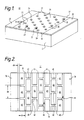
- Figure 1 is a perspective view of a magnetoresistor made in accordance with the present invention; and
- Figure 2 is a top plan view of another magnetoresistor in accordance with the invention. The drawings are not necessarily to scale.
- Referring to Figure 1, there is shown a perspective view of a magnetoresistor 10 in accordance with the present invention. The magnetoresistor 10 comprises a
substrate 12 of an insulating material, such as iron-doped gallium arsenide, having athin film 14 of a degenerately-doped semi-conductor material, such as indium arsenide or indium antimonide, on asurface 16 thereof. Thesemi-conductor film 14, which is the active layer of the magnetoresistor, is of a thickness of no greater than about 5 micrometres, and preferably has a thickness no greater than about 3 micrometres. Thesemi-conductor film 14 is substantially rectangular, and separateconductive contacts substrate surface 16 at opposite edges of thesemi-conductor film 14. Thecontacts semi-conductor film 14. - The
semi-conductor film 14 has a plurality ofopenings 22 therethrough in the form of circular holes which are arranged in spaced parallel rows extending across thefilm 14 parallel to thecontacts holes 22 in alternate rows are arranged between theholes 22 in the adjacent rows. This forms thefilm 14 into a plurality ofspaced paths 24 which extend across thefilm 14 parallel to thecontacts spaced paths 26 which extend between thepaths 24 substantially perpendicular to thecontacts holes 22, i.e., the width of thepaths semi-conductor film 14. Theholes 22 should have a radius such that the perimeter (circumference) of the hole is no greater than the mean free path of electrons in semi-conductor material offilm 14. For example, in gallium arsenide or indium arsenide at room temperature, the mean free path is about 300 nanometres (3000 Angstroms). - In the presence of a magnetic field applied along an axis perpendicular to the surface of the
semi-conductor film 14, the in-plane trajectory of the electrons through thesemi-conductor film 14 and along thepaths semi-conductor film 14 with the radius of the circle, RH, the cyclotron radius, being:
where m is the electron effective mass, v is its total velocity, e is the elemental electron charge, and B is the applied magnetic field. When the magnetic field B is such that the radius R of eachhole 22 equals the cyclotron radius RH, eachhole 22 acts as a minuscule cyclotron, and electrons flow along thepaths holes 22 as indicated by thearrows 28. The electrons so flow until they either re-combine or scatter. This results in an increase in the resistance of the magnetoresistor 10. The field at which this occurs is only a function of the geometry. This is so because the electron effective mass, and its Fermi velocity are parameters which are quite temperature-independent in degenerate semi-conductors. Thus, the magnetoresistor 10 has a high resistance and a low temperature coefficient. - Referring to Figure 2, there is shown a top plan view of another
magnetoresistor 30 in accordance with the present invention. Themagnetoresistor 30 comprises athin film 32 of degenerated semi-conductor material on the surface of aninsulating substrate 34, andconductive contacts semi-conductor film 32. Thesemi-conductor film 32 comprises a plurality of spaced, parallelfirst paths 40 extending parallel to thecontacts second paths 42 extending between thefirst paths 40 substantially perpendicular to thecontacts second paths 42 between two adjacentfirst paths 40 are not aligned with thesecond paths 42 between the next adjacent pairs offirst paths 40 so as to formopenings 43 which are arranged in a substantially staggered brick-work pattern. The spacing N between adjacentfirst paths 40 is no greater than one-third of the mean free path of electrons in thesemi-conductor film 32, and is preferably smaller than one-third of the mean free path. Thespacing 2N between adjacentsecond paths 42 is about twice the spacing between adjacentfirst paths 40. The thickness of thepaths - In the operation of the
magnetoresistor 30, a voltage applied between thecontacts paths semi-conductor film 32, at each intersection of afirst path 40 and asecond path 42, the charge carriers are preferentially steered in one direction in a substantially circular path around a corner or opening 43 by the Lorentz force as indicated by thearrows 44. This blocks the flow of electrons along thesemi-conductor film 32 so as to achieve an increase in the resistance. Thus, the magnetic field applied to themagnetoresistor 30 results in an increase in the magnetoresistance. For the reasons stated with regard to the magnetoresistor 10, themagnetoresistor 30 also has a low temperature coefficient. - The
magnetoresistors 10 and 30 may be made by depositing a film of the semi-conductor material on the surface of a substrate using any suitable chemical vapor-deposition process for the particular material used. Metal contacts are then deposited on the substrate surface at the ends of the semi-conductor film either by evaporation in a vacuum or by sputtering. Theholes 22 in the semi-conductor film of the magnetoresistor 10 and the openings between thepaths magnetoresistor 30 are formed by electron-beam lithography. - Thus, there is provided by the present invention a magnetoresistor in which the paths of the semi-conductor film are designed so that, when a magnetic field is applied to the semi-conductor film, the electrons will flow in a circular path and thereby increase the resistance of the magnetoresistor. The factors which affect this increase in resistance are temperature-independent so that the temperature coefficient of the magnetoresistor is low.
Claims (5)
- A magnetoresistor (10;30) comprising: a thin film (14;32) of a semi-conductor material and a pair of conductive contacts (18,20;36,38) at opposite ends of the film (14;32), said film having openings (22;43) formed therethrough such that, when a magnetic field is applied perpendicular to the semi-conductor film (14;32), the electrical resistance between the conductive contacts (18,20;36,38) increases, characterised in that said semi-conductor material is a degenerately-doped semi-conductor material which is of a thickness no greater than 5 micrometres and which provides a given mean free path of electrons in said thin film (14;32); said openings (22:43) in said semi-conductor film (14;32) form parallel rows of uniformly-shaped openings (22;43) therein, said openings having dimensions small enough to provide an opening perimeter that is not greater than the mean free path of electrons in said semi-conductor film (14;32); said openings (22;43) are spaced apart from one another by a predetermined spacing that is no greater than the mean free path of electrons in the semi-conductor film (14;32); said rows of openings (22;43) provide laterally-spaced paths (26;42) in said semi-conductor film (14;32) which are substantially perpendicular to the conductive contacts (18,20;36,38); said rows of openings (22;43) provide longitudinally-spaced paths (24;40) in said semi-conductive film (14;32) which are substantially parallel to the conductive contacts (18,20;36,38); said spaced paths each have a width not greater than the mean free path of electrons in said semi-conductor film (14;32); and said parallel and perpendicular paths (24,26;40,42) intersect with one another at locations adjacent said openings (22;43) to provide substantially annular paths around said openings (22;43) such that, when said magnetic field is applied perpendicular to the semi-conductor film (14;32), electrons flowing through the semi-conductor film (14;32) between the conductive contacts (18,20;36,38) are caused to flow in said substantially annular paths (28;44) around at least some of said openings (22;43) to thereby increase the electrical resistance between the conductive contacts (18,20;36,38).
- A magnetoresistor (10;30) according to claim 1, in which the openings (22;43) are arranged in rows substantially parallel to the conductive contacts (18,20;36,38) with the openings (22;43) in each row being laterally disposed from and spaced between the openings (22;43) in the adjacent rows.
- A magnetoresistor (10) according to claim 1 or 2, in which the openings are circular holes (22).
- A magnetoresistor (30) according to claim 1 or 2, in which the openings (43) are rectangular in shape, each rectangular opening (43) having a dimension N in the direction perpendicular to the contacts (36,38) that is no greater than one-third the mean free path of electrons through the film (32), and having a dimension parallel to the contacts (36,38) which is equivalent to 2N.
- A magnetoresistor (30) according to claim 4, in which the paths (40,42) of the film (32) have spaced parallel first portions (40) extending parallel to the contacts (36,38) and spaced parallel second portions (42) extending between the first portions (40) to form the rectangular openings (43).
Applications Claiming Priority (2)
| Application Number | Priority Date | Filing Date | Title |
|---|---|---|---|
| US07/483,689 US5038131A (en) | 1990-02-23 | 1990-02-23 | Magnetoresistor |
| US483689 | 1990-02-23 |
Publications (2)
| Publication Number | Publication Date |
|---|---|
| EP0443660A1 EP0443660A1 (en) | 1991-08-28 |
| EP0443660B1 true EP0443660B1 (en) | 1994-11-30 |
Family
ID=23921123
Family Applications (1)
| Application Number | Title | Priority Date | Filing Date |
|---|---|---|---|
| EP91200268A Expired - Lifetime EP0443660B1 (en) | 1990-02-23 | 1991-02-08 | Magnetoresistor |
Country Status (3)
| Country | Link |
|---|---|
| US (1) | US5038131A (en) |
| EP (1) | EP0443660B1 (en) |
| DE (1) | DE69105294T2 (en) |
Families Citing this family (7)
| Publication number | Priority date | Publication date | Assignee | Title |
|---|---|---|---|---|
| US5883564A (en) * | 1994-04-18 | 1999-03-16 | General Motors Corporation | Magnetic field sensor having high mobility thin indium antimonide active layer on thin aluminum indium antimonide buffer layer |
| EP0678925A1 (en) * | 1994-04-18 | 1995-10-25 | General Motors Corporation | Magnetic field sensor |
| US5491461A (en) * | 1994-05-09 | 1996-02-13 | General Motors Corporation | Magnetic field sensor on elemental semiconductor substrate with electric field reduction means |
| US5561079A (en) * | 1994-12-16 | 1996-10-01 | General Motors Corporation | Stalagraphy |
| US6510031B1 (en) * | 1995-03-31 | 2003-01-21 | International Business Machines Corporation | Magnetoresistive sensor with magnetostatic coupling to obtain opposite alignment of magnetic regions |
| US6075437A (en) * | 1998-03-09 | 2000-06-13 | General Motors Corporation | In-plane magnetoresistance bridge |
| JP3651433B2 (en) * | 2001-09-28 | 2005-05-25 | 株式会社村田製作所 | Magnetic sensor |
Family Cites Families (10)
| Publication number | Priority date | Publication date | Assignee | Title |
|---|---|---|---|---|
| GB1309785A (en) * | 1969-05-16 | 1973-03-14 | Exxon Research Engineering Co | Promotor for acid gas absorption |
| US3856921A (en) * | 1970-07-22 | 1974-12-24 | Exxon Research Engineering Co | Promoting scrubbing of acid gases |
| US3931389A (en) * | 1971-06-04 | 1976-01-06 | Metallgesellschaft Aktiengesellschaft | Process of desulfurizing hot gases |
| US3789311A (en) * | 1971-09-13 | 1974-01-29 | Denki Onkyo Co Ltd | Hall effect device |
| US3898359A (en) * | 1974-01-15 | 1975-08-05 | Precision Electronic Component | Thin film magneto-resistors and methods of making same |
| US3989811A (en) * | 1975-01-30 | 1976-11-02 | Shell Oil Company | Process for recovering sulfur from fuel gases containing hydrogen sulfide, carbon dioxide, and carbonyl sulfide |
| US4224594A (en) * | 1978-12-22 | 1980-09-23 | General Electric Company | Deep diode magnetoresistor |
| US4939456A (en) * | 1988-12-23 | 1990-07-03 | General Motors Corporation | Position sensor including a thin film indium arsenide magnetoresistor on a permanent magnet |
| US4978938A (en) * | 1988-12-23 | 1990-12-18 | General Motors Corporation | Magnetoresistor |
| US4926154A (en) * | 1988-12-23 | 1990-05-15 | General Motors Corporation | Indium arsenide magnetoresistor |
-
1990
- 1990-02-23 US US07/483,689 patent/US5038131A/en not_active Expired - Lifetime
-
1991
- 1991-02-08 EP EP91200268A patent/EP0443660B1/en not_active Expired - Lifetime
- 1991-02-08 DE DE69105294T patent/DE69105294T2/en not_active Expired - Fee Related
Also Published As
| Publication number | Publication date |
|---|---|
| DE69105294D1 (en) | 1995-01-12 |
| EP0443660A1 (en) | 1991-08-28 |
| US5038131A (en) | 1991-08-06 |
| DE69105294T2 (en) | 1995-04-13 |
Similar Documents
| Publication | Publication Date | Title |
|---|---|---|
| US5196821A (en) | Integrated magnetic field sensor | |
| KR100696960B1 (en) | Abnormal Magnetoresistance at Room Temperature in Heterogeneous Semiconductors with Narrow Bandgap | |
| EP0698279B1 (en) | Bi-stable memory element | |
| US4939456A (en) | Position sensor including a thin film indium arsenide magnetoresistor on a permanent magnet | |
| US4978938A (en) | Magnetoresistor | |
| EP0443660A1 (en) | Magnetoresistor | |
| DE68919036T2 (en) | Magnetic field sensors. | |
| US20040263163A1 (en) | Sensor structure and magnetic field sensor | |
| KR101423925B1 (en) | Graphene multiple-valued logic device, method for operating the same and method for fabricating the same | |
| US5486804A (en) | Integrated magnetoresistive sensor fabrication method and apparatus | |
| EP3731230A1 (en) | Magnetic element having an improved measurement range | |
| US3617975A (en) | Two-layer magnetoresistors | |
| JPH077195A (en) | Magnetic reluctance converter and preparation thereof | |
| KR950009549A (en) | Magnetoresistive device and magnetic head having the device | |
| US5432494A (en) | Magnetoresistance element | |
| US5646051A (en) | Process for forming a magnetoresistive sensor for a reading head | |
| US5622874A (en) | Process for forming a magnetoresistive sensor for a read/write head | |
| EP0678925A1 (en) | Magnetic field sensor | |
| JPH11317555A (en) | In-plane magnetoresistive bridge | |
| US7741204B2 (en) | Mixed-scale electronic interfaces | |
| JPS6311672Y2 (en) | ||
| CN1705891B (en) | Magnetic field detection device | |
| EP0381541A2 (en) | Superconductive magnetoresistive device | |
| KR100629676B1 (en) | Gate control Hall effect device and method of manufacturing the same | |
| JP2962293B2 (en) | Corbino type magnetic sensor |
Legal Events
| Date | Code | Title | Description |
|---|---|---|---|
| PUAI | Public reference made under article 153(3) epc to a published international application that has entered the european phase |
Free format text: ORIGINAL CODE: 0009012 |
|
| AK | Designated contracting states |
Kind code of ref document: A1 Designated state(s): DE FR NL |
|
| 17P | Request for examination filed |
Effective date: 19911004 |
|
| 17Q | First examination report despatched |
Effective date: 19931001 |
|
| GRAA | (expected) grant |
Free format text: ORIGINAL CODE: 0009210 |
|
| AK | Designated contracting states |
Kind code of ref document: B1 Designated state(s): DE FR NL |
|
| REF | Corresponds to: |
Ref document number: 69105294 Country of ref document: DE Date of ref document: 19950112 |
|
| ET | Fr: translation filed | ||
| PLBE | No opposition filed within time limit |
Free format text: ORIGINAL CODE: 0009261 |
|
| STAA | Information on the status of an ep patent application or granted ep patent |
Free format text: STATUS: NO OPPOSITION FILED WITHIN TIME LIMIT |
|
| 26N | No opposition filed | ||
| PGFP | Annual fee paid to national office [announced via postgrant information from national office to epo] |
Ref country code: DE Payment date: 19991231 Year of fee payment: 10 |
|
| PGFP | Annual fee paid to national office [announced via postgrant information from national office to epo] |
Ref country code: FR Payment date: 20000217 Year of fee payment: 10 |
|
| PGFP | Annual fee paid to national office [announced via postgrant information from national office to epo] |
Ref country code: NL Payment date: 20000229 Year of fee payment: 10 |
|
| PG25 | Lapsed in a contracting state [announced via postgrant information from national office to epo] |
Ref country code: NL Free format text: LAPSE BECAUSE OF NON-PAYMENT OF DUE FEES Effective date: 20010901 |
|
| PG25 | Lapsed in a contracting state [announced via postgrant information from national office to epo] |
Ref country code: FR Free format text: LAPSE BECAUSE OF NON-PAYMENT OF DUE FEES Effective date: 20011031 |
|
| NLV4 | Nl: lapsed or anulled due to non-payment of the annual fee |
Effective date: 20010901 |
|
| REG | Reference to a national code |
Ref country code: FR Ref legal event code: ST |
|
| PG25 | Lapsed in a contracting state [announced via postgrant information from national office to epo] |
Ref country code: DE Free format text: LAPSE BECAUSE OF NON-PAYMENT OF DUE FEES Effective date: 20011201 |