EP0442286B1 - Power factor correction circuit - Google Patents
Power factor correction circuit Download PDFInfo
- Publication number
- EP0442286B1 EP0442286B1 EP91100679A EP91100679A EP0442286B1 EP 0442286 B1 EP0442286 B1 EP 0442286B1 EP 91100679 A EP91100679 A EP 91100679A EP 91100679 A EP91100679 A EP 91100679A EP 0442286 B1 EP0442286 B1 EP 0442286B1
- Authority
- EP
- European Patent Office
- Prior art keywords
- signal
- produce
- coupled
- voltage
- current
- Prior art date
- Legal status (The legal status is an assumption and is not a legal conclusion. Google has not performed a legal analysis and makes no representation as to the accuracy of the status listed.)
- Expired - Lifetime
Links
Images

Classifications
-
- H—ELECTRICITY
- H02—GENERATION; CONVERSION OR DISTRIBUTION OF ELECTRIC POWER
- H02M—APPARATUS FOR CONVERSION BETWEEN AC AND AC, BETWEEN AC AND DC, OR BETWEEN DC AND DC, AND FOR USE WITH MAINS OR SIMILAR POWER SUPPLY SYSTEMS; CONVERSION OF DC OR AC INPUT POWER INTO SURGE OUTPUT POWER; CONTROL OR REGULATION THEREOF
- H02M1/00—Details of apparatus for conversion
- H02M1/42—Circuits or arrangements for compensating for or adjusting power factor in converters or inverters
- H02M1/4208—Arrangements for improving power factor of AC input
- H02M1/4225—Arrangements for improving power factor of AC input using a non-isolated boost converter
-
- H—ELECTRICITY
- H05—ELECTRIC TECHNIQUES NOT OTHERWISE PROVIDED FOR
- H05B—ELECTRIC HEATING; ELECTRIC LIGHT SOURCES NOT OTHERWISE PROVIDED FOR; CIRCUIT ARRANGEMENTS FOR ELECTRIC LIGHT SOURCES, IN GENERAL
- H05B41/00—Circuit arrangements or apparatus for igniting or operating discharge lamps
- H05B41/14—Circuit arrangements
- H05B41/26—Circuit arrangements in which the lamp is fed by power derived from dc by means of a converter, e.g. by high-voltage dc
- H05B41/28—Circuit arrangements in which the lamp is fed by power derived from dc by means of a converter, e.g. by high-voltage dc using static converters
-
- Y—GENERAL TAGGING OF NEW TECHNOLOGICAL DEVELOPMENTS; GENERAL TAGGING OF CROSS-SECTIONAL TECHNOLOGIES SPANNING OVER SEVERAL SECTIONS OF THE IPC; TECHNICAL SUBJECTS COVERED BY FORMER USPC CROSS-REFERENCE ART COLLECTIONS [XRACs] AND DIGESTS
- Y02—TECHNOLOGIES OR APPLICATIONS FOR MITIGATION OR ADAPTATION AGAINST CLIMATE CHANGE
- Y02B—CLIMATE CHANGE MITIGATION TECHNOLOGIES RELATED TO BUILDINGS, e.g. HOUSING, HOUSE APPLIANCES OR RELATED END-USER APPLICATIONS
- Y02B70/00—Technologies for an efficient end-user side electric power management and consumption
- Y02B70/10—Technologies improving the efficiency by using switched-mode power supplies [SMPS], i.e. efficient power electronics conversion e.g. power factor correction or reduction of losses in power supplies or efficient standby modes
Definitions
- the present invention concerns a ballast circuit according to the introductory portion of claim 1 and a method according to the introductory portion of claim 3.
- Ballast circuitry within a fluorescent lamp system is used to convert an incoming AC voltage signal to a high DC voltage signal.
- the incoming AC voltage signal typically has a RMS voltage of either 120 volts or 277 volts.
- the high DC voltage is converted to a high frequency AC voltage which is applied to a series resonant/lamp circuit.
- the amplitude of the current drawn from the incoming AC voltage signal should be in phase with the amplitude of the voltage of the incoming AC voltage signal.
- a control circuit generates an output signal, the frequency of which is controlled to maintain the output voltage of the switching regulator at a substantially constant level and the pulse width of which is controlled such that the current drawn by the regulator is substantially sinusoidal.
- US-A-4 412 277 discloses an AC to DC converter for converting an AC signal to a DC signal under the control of a control signal.
- the control signal is generated by a control circuit that includes a first analog generator that provides a first signal analog to the voltage of the AC signal to be converted.
- a second analog generator generates a second signal analog to the current of the AC signal and a third analog generator generates a third signal analog to the voltage of the DC output signal.
- the third and the first signals are multiplied together to obtain a fourth signal.
- the control signal is generated by the comparison of the fourth signal with the second signal to obtain a difference signal which is then compared with a high frequency sawtooth waveform and is used to generate the control signal for driving the AC to DC converter.
- GB-A-2 213 614 describes a waveform control arrangement for a switched mode power supply.
- a control arrangement for interfacing a DC-DC converter in the power supply with a mains power supply includes a semiconductor switch for controlling the input current to the arrangement to have the same waveform as the input voltage to the arrangement.
- the duty ratio of the semiconductor switch is controlled in dependence on a predetermined relation between a predetermined time-varying signal generated by a sawtooth circuit and a signal derived from the input current.
- An output voltage error signal controls the peak amplitude of the sawtooth signal.
- the problem underlying the present invention is to provide inexpensive ballast circuitry which allows for high power conservation.
- the problem is solved by the ballast circuit as characterized in claim 1 and the method as characterized in claim 3.
- a ballast circuit for producing a DC signal with a high voltage amplitude is presented.
- a capacitor connected to a circuit output stores a charge which provides the high voltage amplitude of the DC signal.
- Current from an inductor is used to charge the capacitor.
- a current gate when it is turned on, drains current from the inductor. Energy is thus stored in the inductor when the current gate is turned on.
- the current gate When the current gate is turned off, current from the inductor charges the capacitor.
- a control circuit turns the current gate on and off so that the amplitude of the current drawn from the incoming AC voltage signal is in phase with the amplitude of the voltage of the incoming AC voltage signal.
- the control circuit includes a ramp generator which generates a pulse modulation reference signal with a varying voltage amplitude and a comparator which compares the pulse modulation reference signal with the incoming AC voltage signal after the incoming AC voltage signal has been rectified and the voltage divided by a voltage divider. The comparator produces a first modulated signal.
- the control circuit also includes a second comparator which compares the pulse modulation reference signal with a feedback signal to produce a second modulated signal.
- the feedback signal is proportional to the DC signal.
- a logical AND is performed on the first modulated and the second modulated signal.
- the resultant signal is then amplified to produce a control signal which is used to turn the current gate on and off.
- the control circuit is inexpensive to manufacture and yet allows the ballast circuit to accomplish the goal of drawing off current from the incoming AC voltage signal in phase with the amplitude of the voltage of the incoming AC voltage signal.
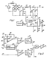
- FIG. 1 shows ballast circuitry in accordance with a preferred embodiment of the present invention.
- FIG. 2 shows a block diagram of a correction circuit within the ballast circuitry of Figure 1, in accordance with the preferred embodiment of the present invention.
- Figure 3 shows voltage amplitude as a function of time for various signals within the correction circuit of Figure 2 in accordance with the preferred embodiment of the present invention.
- FIG. 1 ballast circuitry which is used in a fluorescent lamp system.
- An AC signal source 10 represents the AC signal from a power source such as a standard electrical outlet.
- the RMS voltage of the AC signal is typically 120 volts or 277 volts.
- An inductor 11 is used to provide input inductance to the incoming AC voltage signal before the AC signal is connected to a rectifier 12.
- Rectifier 12 consists of rectifiers 13, 14, 15 and 16 connected as shown. Rectifier 12 produces a rectified AC signal which is placed on a line 37.
- Capacitor 23 is charged by current provided from an inductor 20 through a diode 21. When the AC signal from AC signal source 10 is at greater voltage amplitudes, current energy is stored in inductor 20. When the AC signal is at lesser voltage amplitudes, energy stored in inductor 20 is used to charge capacitor 23. A capacitor 17 is used to store charge utilized to maintain current through inductor 20.
- Energy is stored within inductor 20 by turning on a gate 22.
- gate 22 When gate 22 is turned on, an end 38 of inductor 20 is connected to a ground 28. This causes energy in the form of current flow to be stored in inductor 20.
- gate 22 When gate 22 is turned off, this current is forced to flow through diode 21 and to charge capacitor 23.
- Gate 22 is switched on and off by a control signal on a line 31. The control signal is generated by a correction circuit 24. Correction circuit 24 causes gate 22 to be switched on and off in a pattern such that current drawn from AC signal source 10 varies synchronously with the voltage amplitude of the AC signal from AC signal source 10.
- Correction circuit 24 receives on a line 33 a clock signal from a clock 27. Correction circuit 24 receives on a line 32 a voltage divided signal based on the rectified AC signal. The voltage amplitude of the rectified AC signal is proportionately reduced by a voltage divider consisting of a resistor 18 and a resistor 19.
- Correction circuit 24 also receives as feedback the high DC level signal on line 30.
- the high DC level signal on line 30 may be, for example, set at 300 volts.
- the high DC level signal on line 30 may be, for example, set at 450 volts.
- the high DC level signal is proportionately reduced by a voltage divider consisting of a resistor 25 within correction circuit 24 and a resistor 26 external to correction circuit 24.
- the divided feedback voltage is placed on a line 34.
- Power to correction circuit 24 is supplied by a DC voltage placed on a line 35 by a DC power source 29.
- Correction circuit 24 is also connected to ground 28.
- Correction circuit 24 may be inhibited/enabled by an inhibit/enable signal placed on a line 36.
- FIG. 2 shows a block diagram of correction circuit 24.
- a ramp generator 42 receives the clock signal on line 33 and produces a ramp signal on a line 61.
- the ramp signal on line 61 is used as input to a comparator 43 and a comparator 44.
- Comparator 44 compares the ramp signal with the relative voltage amplitude of the rectified AC signal on line 32.
- the output signal of comparator 44 may be latched by an RS latch 46.
- the output signal of RS latch 46 is placed on a line 64.
- the clock signal on line 33 is used to reset RS latch 46.
- Comparator 43 compares the ramp signal with an amplified signal on line 62 generated by an "Error" amplifier 41.
- Error amplifier 41 has a gain of approximately 10.
- the voltage of the amplified signal on line 62 is proportional to the voltage differential between the divided feedback voltage on line 34 and an internal reference voltage.
- the internal reference voltage is determined by a voltage divider consisting of a resistor 50 and a resistor 51 connected between line 35 and ground 28. Resistors 50 and 51 are internal to correction circuit 24 so that voltage at a location 65 is approximately 14.5 volts.
- a capacitor 49 is connected as shown in order to provide negative feedback to amplifier 41 in order to prevent oscillation. Capacitor 49 may be for example 1 microfarad (16 volts).
- the output signal of comparator 43 may be latched by an RS latch 45.
- the output signal of RS latch 45 is placed on a line 63.
- the clock signal on line 33 is used to reset RS latch 45.
- a logical AND gate 47 receives as input the signal on line 63 and the signal on line 64.
- the output of logical AND gate 47 is amplified by an amplifier 48 to produce the control signal on line 31.
- the inhibit/enable signal on line 36 is used to inhibit/enable logical AND gate 47 as shown.
- Figure 3 shows voltage amplitude on an axis 102 as a function of time on an axis 101 for various signals within correction circuit 24.
- a voltage amplitude 132 is the voltage amplitude of the voltage divided signal on line 32 and is proportional to the voltage amplitude of the rectified AC signal on line 37.
- a voltage amplitude 161 is the voltage amplitude of the ramp signal on line 61.
- a voltage amplitude 164 is the voltage amplitude of the output signal of RS latch 46 placed on line 64.
- a voltage amplitude 163 is the voltage amplitude of the output signal of RS latch 45 placed on line 63.
- a voltage amplitude 131 is the voltage amplitude of the control signal on line 31.
- Voltage amplitude 131 is obtained as a result of performing a logical AND of voltage amplitude 163 and voltage amplitude 164.
- the amplitude of the current drawn from AC signal source 10 is in phase with the amplitude of the voltage of AC signal source 10.
- the following values may be used for the components shown in Figure 2.
- Inductor 11 is 1.25 millihenries.
- Diodes 13, 14, 15 and 16 are type 1N4003.
- Capacitor 17 is 1.0 micro farads (250 volts).
- Inductor 20 is 0.750 millihenries.
- Resistor 18 is 430 kilohms.
- Resistor 19 is 10 kilohms.
- Gate 22 is type IRF 720, available from Siliconix Inc., having a business address of 2201 Laurelwood Road, Santa Clara, CA 95056.
- Diode 21 is type FR105 available from Diodes Inc., having a business address of 9957 Canoga Avenue, chatsworth, CA 91311.
- Capacitor 23 is 22 microfarads (350 volts).
- Resistor 25 is 510 kilohms.
- Resistor 26 is 16.3 kilohms.
- Inductor 11 is 1.25 millihenries.
- Diodes 13, 14, 15 and 16 are type 1N4005.
- Capacitor 17 is 0.33 micro farads (450 volts).
- Inductor 20 is 0.450 millihenries.
- Resistor 18 is 430 kilohms.
- Resistor 19 is 3.6 kilohms.
- Gate 22 is type IRF 820.
- Diode 21 is type FR105 available from Diodes Inc.
- Capacitor 23 is 33 microfarads (450 volts).
- Resistor 25 is 510 kilohms.
- Resistor 26 is 23.6 kilohms.
Description
- The present invention concerns a ballast circuit according to the introductory portion of claim 1 and a method according to the introductory portion of claim 3.
- Ballast circuitry within a fluorescent lamp system is used to convert an incoming AC voltage signal to a high DC voltage signal. The incoming AC voltage signal typically has a RMS voltage of either 120 volts or 277 volts. The high DC voltage is converted to a high frequency AC voltage which is applied to a series resonant/lamp circuit.
- In order to best conserve power, the amplitude of the current drawn from the incoming AC voltage signal should be in phase with the amplitude of the voltage of the incoming AC voltage signal.
- From WO-A-85 01400 there is prior known a switching regulator circuit corresponding to the ballast circuit according to the introductory portion of claim 1. A control circuit generates an output signal, the frequency of which is controlled to maintain the output voltage of the switching regulator at a substantially constant level and the pulse width of which is controlled such that the current drawn by the regulator is substantially sinusoidal.
- US-A-4 412 277 discloses an AC to DC converter for converting an AC signal to a DC signal under the control of a control signal. The control signal is generated by a control circuit that includes a first analog generator that provides a first signal analog to the voltage of the AC signal to be converted. A second analog generator generates a second signal analog to the current of the AC signal and a third analog generator generates a third signal analog to the voltage of the DC output signal. The third and the first signals are multiplied together to obtain a fourth signal. The control signal is generated by the comparison of the fourth signal with the second signal to obtain a difference signal which is then compared with a high frequency sawtooth waveform and is used to generate the control signal for driving the AC to DC converter.
- GB-A-2 213 614 describes a waveform control arrangement for a switched mode power supply. A control arrangement for interfacing a DC-DC converter in the power supply with a mains power supply includes a semiconductor switch for controlling the input current to the arrangement to have the same waveform as the input voltage to the arrangement. The duty ratio of the semiconductor switch is controlled in dependence on a predetermined relation between a predetermined time-varying signal generated by a sawtooth circuit and a signal derived from the input current. An output voltage error signal controls the peak amplitude of the sawtooth signal.
- The problem underlying the present invention is to provide inexpensive ballast circuitry which allows for high power conservation. The problem is solved by the ballast circuit as characterized in claim 1 and the method as characterized in claim 3.
- In accordance with the preferred embodiment of the present invention, a ballast circuit for producing a DC signal with a high voltage amplitude is presented. In the ballast circuit, a capacitor connected to a circuit output stores a charge which provides the high voltage amplitude of the DC signal. Current from an inductor is used to charge the capacitor. A current gate, when it is turned on, drains current from the inductor. Energy is thus stored in the inductor when the current gate is turned on. When the current gate is turned off, current from the inductor charges the capacitor.
- A control circuit turns the current gate on and off so that the amplitude of the current drawn from the incoming AC voltage signal is in phase with the amplitude of the voltage of the incoming AC voltage signal. The control circuit includes a ramp generator which generates a pulse modulation reference signal with a varying voltage amplitude and a comparator which compares the pulse modulation reference signal with the incoming AC voltage signal after the incoming AC voltage signal has been rectified and the voltage divided by a voltage divider. The comparator produces a first modulated signal.
- The control circuit also includes a second comparator which compares the pulse modulation reference signal with a feedback signal to produce a second modulated signal. The feedback signal is proportional to the DC signal. A logical AND is performed on the first modulated and the second modulated signal. The resultant signal is then amplified to produce a control signal which is used to turn the current gate on and off.
- The control circuit is inexpensive to manufacture and yet allows the ballast circuit to accomplish the goal of drawing off current from the incoming AC voltage signal in phase with the amplitude of the voltage of the incoming AC voltage signal.
- Figure 1 shows ballast circuitry in accordance with a preferred embodiment of the present invention.
- Figure 2 shows a block diagram of a correction circuit within the ballast circuitry of Figure 1, in accordance with the preferred embodiment of the present invention.
- Figure 3 shows voltage amplitude as a function of time for various signals within the correction circuit of Figure 2 in accordance with the preferred embodiment of the present invention.
- In Figure 1 is shown ballast circuitry which is used in a fluorescent lamp system. An
AC signal source 10 represents the AC signal from a power source such as a standard electrical outlet. The RMS voltage of the AC signal is typically 120 volts or 277 volts. An inductor 11 is used to provide input inductance to the incoming AC voltage signal before the AC signal is connected to a rectifier 12. Rectifier 12 consists ofrectifiers line 37. - Charge stored within a
capacitor 23 is used to provide a high DC level signal on aline 30.Capacitor 23 is charged by current provided from aninductor 20 through adiode 21. When the AC signal fromAC signal source 10 is at greater voltage amplitudes, current energy is stored ininductor 20. When the AC signal is at lesser voltage amplitudes, energy stored ininductor 20 is used to chargecapacitor 23. Acapacitor 17 is used to store charge utilized to maintain current throughinductor 20. - Energy is stored within
inductor 20 by turning on agate 22. Whengate 22 is turned on, anend 38 ofinductor 20 is connected to aground 28. This causes energy in the form of current flow to be stored ininductor 20. Whengate 22 is turned off, this current is forced to flow throughdiode 21 and to chargecapacitor 23.Gate 22 is switched on and off by a control signal on aline 31. The control signal is generated by acorrection circuit 24.Correction circuit 24 causesgate 22 to be switched on and off in a pattern such that current drawn fromAC signal source 10 varies synchronously with the voltage amplitude of the AC signal fromAC signal source 10. -
Correction circuit 24 receives on a line 33 a clock signal from aclock 27.correction circuit 24 receives on a line 32 a voltage divided signal based on the rectified AC signal. The voltage amplitude of the rectified AC signal is proportionately reduced by a voltage divider consisting of aresistor 18 and aresistor 19. -
Correction circuit 24 also receives as feedback the high DC level signal online 30. When the RMS voltage ofAC signal source 10 is 120 volts, the high DC level signal online 30 may be, for example, set at 300 volts. When the RMS voltage ofAC signal source 10 is 277 volts, the high DC level signal online 30 may be, for example, set at 450 volts. - The high DC level signal is proportionately reduced by a voltage divider consisting of a
resistor 25 withincorrection circuit 24 and aresistor 26 external tocorrection circuit 24. The divided feedback voltage is placed on aline 34. Power tocorrection circuit 24 is supplied by a DC voltage placed on aline 35 by aDC power source 29.Correction circuit 24 is also connected toground 28.Correction circuit 24 may be inhibited/enabled by an inhibit/enable signal placed on aline 36. - Figure 2 shows a block diagram of
correction circuit 24. Aramp generator 42 receives the clock signal online 33 and produces a ramp signal on aline 61. The ramp signal online 61 is used as input to acomparator 43 and acomparator 44.Comparator 44 compares the ramp signal with the relative voltage amplitude of the rectified AC signal online 32. In order to prevent noise online 32 from causing oscillation in the output ofcomparator 44, the output signal ofcomparator 44 may be latched by anRS latch 46. The output signal of RS latch 46 is placed on a line 64. The clock signal online 33 is used to resetRS latch 46. -
Comparator 43 compares the ramp signal with an amplified signal online 62 generated by an "Error" amplifier 41. Error amplifier 41 has a gain of approximately 10. The voltage of the amplified signal online 62 is proportional to the voltage differential between the divided feedback voltage online 34 and an internal reference voltage. The internal reference voltage is determined by a voltage divider consisting of aresistor 50 and aresistor 51 connected betweenline 35 andground 28.Resistors correction circuit 24 so that voltage at alocation 65 is approximately 14.5 volts. Acapacitor 49 is connected as shown in order to provide negative feedback to amplifier 41 in order to prevent oscillation.Capacitor 49 may be for example 1 microfarad (16 volts). In order to preventnoise oil line 62 from causing oscillation in the output ofcomparator 43, the output signal ofcomparator 43 may be latched by anRS latch 45. The output signal of RS latch 45 is placed on aline 63. The clock signal online 33 is used to resetRS latch 45. - A logical AND
gate 47 receives as input the signal online 63 and the signal on line 64. The output of logical ANDgate 47 is amplified by anamplifier 48 to produce the control signal online 31. The inhibit/enable signal online 36 is used to inhibit/enable logical ANDgate 47 as shown. - Figure 3 shows voltage amplitude on an
axis 102 as a function of time on anaxis 101 for various signals withincorrection circuit 24. Avoltage amplitude 132 is the voltage amplitude of the voltage divided signal online 32 and is proportional to the voltage amplitude of the rectified AC signal online 37. Avoltage amplitude 161 is the voltage amplitude of the ramp signal online 61. Avoltage amplitude 164 is the voltage amplitude of the output signal of RS latch 46 placed on line 64. Avoltage amplitude 163 is the voltage amplitude of the output signal of RS latch 45 placed online 63. Avoltage amplitude 131 is the voltage amplitude of the control signal online 31. - As may be seen from Figure 3, when
voltage amplitude 161 is greater thanvoltage amplitude 132,voltage amplitude 164 is at a logic 1. Otherwise,voltage amplitude 164 is at a logic 0.Voltage amplitude 131 is obtained as a result of performing a logical AND ofvoltage amplitude 163 andvoltage amplitude 164. - As may be seen from Figure 3, the higher the value of
voltage amplitude 132, the shorter theduration voltage amplitude 131 is at logic 1. The implication of this is that when the voltage amplitude of the rectified signal online 37 is at a maximum,gate 22 is primarily turned off. When the voltage amplitude of the rectified signal online 37 is at a minimum,gate 22 is primarily turned on and energy is being stored withininductor 20 in order to chargecapacitor 23 whengate 22 is turned off. - When the components of the ballast circuitry are chosen appropriately, it is possible to cause the amplitude of the current drawn from
AC signal source 10 to be in phase with the amplitude of the voltage ofAC signal source 10. For example, when the RMS voltage ofAC signal source 10 is 120 volts the following values may be used for the components shown in Figure 2. Inductor 11 is 1.25 millihenries.Diodes Capacitor 17 is 1.0 micro farads (250 volts).Inductor 20 is 0.750 millihenries.Resistor 18 is 430 kilohms.Resistor 19 is 10 kilohms.Gate 22 is type IRF 720, available from Siliconix Inc., having a business address of 2201 Laurelwood Road, Santa Clara, CA 95056.Diode 21 is type FR105 available from Diodes Inc., having a business address of 9957 Canoga Avenue, chatsworth, CA 91311.Capacitor 23 is 22 microfarads (350 volts).Resistor 25 is 510 kilohms.Resistor 26 is 16.3 kilohms. - When the RMS voltage of
AC signal source 10 is 277 volts the following values may be used for the components shown in Figure 2. Inductor 11 is 1.25 millihenries.Diodes Capacitor 17 is 0.33 micro farads (450 volts).Inductor 20 is 0.450 millihenries.Resistor 18 is 430 kilohms.Resistor 19 is 3.6 kilohms.Gate 22 is type IRF 820.Diode 21 is type FR105 available from Diodes Inc.Capacitor 23 is 33 microfarads (450 volts).Resistor 25 is 510 kilohms.Resistor 26 is 23.6 kilohms.
Claims (4)
- A ballast circuit for producing on a circuit output a DC signal with a high voltage amplitude, the ballast circuit comprising:
a power source (10) for providing an AC signal,
rectifying means (12), coupled to the power source, for rectifying the AC signal to produce a rectified AC signal,
voltage dividing means (18, 19), coupled to the rectifying means (12), for dividing voltage of the rectified AC signal to produce a voltage divided signal,
capacitance means (23), coupled to the circuit output, for storing a charge,
inductance means (20), coupled to the rectifying means (12), for providing a current to charge the capacitance means (23),
diode means (21), coupled between the capacitance means (23) and the inductance means (20), for allowing current to flow from the inductance means to the capacitance means to charge the capacitance means, and for not allowing current to flow from the capacitance means to the inductance means,
current gate means (22) for draining current from the inductance means (20) when the current gate means is turned on, and
control circuitry (24), coupled to the current gate means (22) for turning the current gate means on and off,
characterized in that
the control circuitry including
ramp generator means (42) for generating a pulse modulation reference signal with a varying voltage amplitude, and
first comparator means (44), coupled to the ramp generator (42) and to the voltage divider (18, 19), for comparing the pulse modulation reference signal with the voltage divided signal to produce a first modulated signal,
feedback means (34), coupled to the circuit output for generating a feedback signal based on the high voltage amplitude of the DC signal,
second comparator means (43), coupled to the feedback means (34) and to the ramp generator means (42), for comparing the feedback signal with the pulse modulation reference signal to produce a second modulated signal, and
summing means (47) for performing a logical AND function on the first modulated signal and the second modulated signal to produce a control voltage used for turning the current gate means (22) on and off. - A ballast circuit as in claim 1,
wherein the summing means includes:
first latch means (46), coupled to the first comparator means (44), for latching output of the first comparator means to produce a first latched signal,
secondss latch means (45), coupled to the second comparator means (43), for latching output of the second comparator means to produce a second latched signal,
logic gate means (47), coupled to the first latch means (46) and to the second latch means (45), for performing a logical AND on the first latched signal and the second lateched signal to produce an unamplified control signal, and
amplification means (48), coupled to the logic gate means (47) and to the current gate means (22) for amplifying the unamplified control signal to produce an amplified signal used to control the current gate means. - A method for turning on and off a current gate (22) in a ballast circuit for producing on a circuit output a DC signal with a high voltage amplitude, the ballast circuit including an input for receiving an AC signal, a capacitor (23), coupled to the circuit output for storing a charge, an indicator (20), coupled to the input, which provides a current to charge the capacitor (23), the current gate (22) for draining current from the inductor when the current gate is turned on,
the method characterized by the steps of:(a) generating a pulse modulation reference signal with a varying voltage amplitude,(b) comparing the pulse modulation reference signal with a voltage divided signal to produce a first modulated signal, wherein the first modulated signal is used in generating a control voltage used to switch the current gate on and off and wherein the voltage divided signal is a voltage amplitude proportional to the absolute value of a voltage amplitude of the AC signal,(c) generating a feedback signal based on the high voltage amplitude of the DC signal,(d) comparing a feedback signal with the pulse modulation reference signal to produce a second modulated signal, and(e) performing a logical AND function on the first modulated signal and the second modulated signal to produce the control voltage. - A method as in claim 3
wherein step (e) comprises the substeps of:(e1) latching output of a first comparator means (44) to produce a first latched signal,(e2) latching output of a second comparator means (43) to produce a second latching signal,(e3) performing a logical AND on the first latched signal and the second latched signal to produce an unamplified control signal, and(e4) amplifying the unamplified control signal to produce an amplified signal used to control the current gate.
Applications Claiming Priority (2)
| Application Number | Priority Date | Filing Date | Title |
|---|---|---|---|
| US479650 | 1990-02-14 | ||
| US07/479,650 US5008599A (en) | 1990-02-14 | 1990-02-14 | Power factor correction circuit |
Publications (3)
| Publication Number | Publication Date |
|---|---|
| EP0442286A2 EP0442286A2 (en) | 1991-08-21 |
| EP0442286A3 EP0442286A3 (en) | 1992-04-08 |
| EP0442286B1 true EP0442286B1 (en) | 1995-05-03 |
Family
ID=23904855
Family Applications (1)
| Application Number | Title | Priority Date | Filing Date |
|---|---|---|---|
| EP91100679A Expired - Lifetime EP0442286B1 (en) | 1990-02-14 | 1991-01-21 | Power factor correction circuit |
Country Status (5)
| Country | Link |
|---|---|
| US (1) | US5008599A (en) |
| EP (1) | EP0442286B1 (en) |
| JP (1) | JPH04217870A (en) |
| CA (1) | CA2034799A1 (en) |
| DE (1) | DE69109325D1 (en) |
Families Citing this family (16)
| Publication number | Priority date | Publication date | Assignee | Title |
|---|---|---|---|---|
| US5430354A (en) * | 1992-03-24 | 1995-07-04 | North American Philips Corporation | HID lamp and auxiliary lamp ballast using a single multiple function switch |
| US5258692A (en) * | 1992-06-02 | 1993-11-02 | Appliance Control Technology, Inc. | Electronic ballast high power factor for gaseous discharge lamps |
| KR940007716B1 (en) * | 1992-07-03 | 1994-08-24 | 삼성전자 주식회사 | Continuous current control type power factor correct circuit |
| US5373215A (en) * | 1993-07-07 | 1994-12-13 | The United States Of America As Represented By The United States Department Of Energy | Ionization tube simmer current circuit |
| US5461303A (en) * | 1994-01-31 | 1995-10-24 | Power Integrations, Inc. | Power factor correction precompensation circuit |
| JP3315008B2 (en) * | 1994-06-28 | 2002-08-19 | 松下電工株式会社 | Discharge lamp lighting device |
| AU664153B3 (en) * | 1995-06-30 | 1995-11-02 | Jin Chung Lee | High power factor electrical stabilizer with protection circuit application |
| JPH09172779A (en) * | 1995-07-11 | 1997-06-30 | Meidensha Corp | Sine wave input converter circuit |
| US5661645A (en) | 1996-06-27 | 1997-08-26 | Hochstein; Peter A. | Power supply for light emitting diode array |
| US5894200A (en) * | 1997-03-26 | 1999-04-13 | Goodale, Jr.; Garold Joseph | Two terminal method of and apparatus for improving electrical and light producing efficiency in low voltage direct current incandescent lamp intensity control |
| US6150771A (en) * | 1997-06-11 | 2000-11-21 | Precision Solar Controls Inc. | Circuit for interfacing between a conventional traffic signal conflict monitor and light emitting diodes replacing a conventional incandescent bulb in the signal |
| JPH1167471A (en) * | 1997-08-26 | 1999-03-09 | Tec Corp | Lighting system |
| WO2009025517A2 (en) * | 2007-08-22 | 2009-02-26 | Silicon Mitus, Inc. | Power factor correction circuit |
| DE102010042020A1 (en) * | 2010-10-06 | 2012-04-12 | Osram Ag | Circuit and method for controlling a lamp |
| JP5327251B2 (en) * | 2011-02-28 | 2013-10-30 | Tdk株式会社 | LED lighting device |
| US9955547B2 (en) | 2013-03-14 | 2018-04-24 | Lutron Electronics Co., Inc. | Charging an input capacitor of a load control device |
Family Cites Families (5)
| Publication number | Priority date | Publication date | Assignee | Title |
|---|---|---|---|---|
| EP0059053A3 (en) * | 1981-02-21 | 1983-05-18 | THORN EMI plc | Switched mode power supply |
| US4412277A (en) * | 1982-09-03 | 1983-10-25 | Rockwell International Corporation | AC-DC Converter having an improved power factor |
| NZ209570A (en) * | 1983-09-19 | 1988-03-30 | Minitronics Pty Ltd | Switching regulator |
| GB8800527D0 (en) * | 1988-01-11 | 1988-02-10 | Farnell Instr Ltd | Control arrangement for switched mode power supply |
| US4952849A (en) * | 1988-07-15 | 1990-08-28 | North American Philips Corporation | Fluorescent lamp controllers |
-
1990
- 1990-02-14 US US07/479,650 patent/US5008599A/en not_active Expired - Fee Related
-
1991
- 1991-01-21 DE DE69109325T patent/DE69109325D1/en not_active Expired - Lifetime
- 1991-01-21 EP EP91100679A patent/EP0442286B1/en not_active Expired - Lifetime
- 1991-01-23 CA CA002034799A patent/CA2034799A1/en not_active Abandoned
- 1991-02-13 JP JP3020041A patent/JPH04217870A/en active Pending
Also Published As
| Publication number | Publication date |
|---|---|
| DE69109325D1 (en) | 1995-06-08 |
| CA2034799A1 (en) | 1991-08-15 |
| EP0442286A2 (en) | 1991-08-21 |
| EP0442286A3 (en) | 1992-04-08 |
| JPH04217870A (en) | 1992-08-07 |
| US5008599A (en) | 1991-04-16 |
Similar Documents
| Publication | Publication Date | Title |
|---|---|---|
| EP0442286B1 (en) | Power factor correction circuit | |
| US6275018B1 (en) | Switching power converter with gated oscillator controller | |
| US7064527B2 (en) | Transition mode operating device for the correction of the power factor in switching power supply units | |
| US5949229A (en) | Power factor correction circuit having an error signal multiplied by a current signal | |
| US6034513A (en) | System and method for controlling power factor and power converter employing the same | |
| US5592128A (en) | Oscillator for generating a varying amplitude feed forward PFC modulation ramp | |
| US5642267A (en) | Single-stage, unity power factor switching converter with voltage bidirectional switch and fast output regulation | |
| US6028776A (en) | Power factor correction converter | |
| US5903452A (en) | Adaptive slope compensator for current mode power converters | |
| US4885675A (en) | Transformer isolated AC to DC power conditioner with resistive input current | |
| US7307405B2 (en) | Transition mode operating device for the correction of the power factor in switching power supply units | |
| US6510062B2 (en) | Method and circuit to bias output-side width modulation control in an isolating voltage converter system | |
| JP3175663B2 (en) | Self-oscillation type switching power supply | |
| EP0383815A1 (en) | Current mode converter with controlled slope compensation | |
| JP2001095254A (en) | Series resonance converter with control circuit | |
| JPH11122926A (en) | Self-oscillating switching power supply | |
| US4325113A (en) | High voltage power supply | |
| JP2003125582A (en) | Power unit | |
| JPH06500227A (en) | How to control voltage converter | |
| JP2003125585A (en) | Power unit | |
| JPH06233541A (en) | Switching regulator | |
| EP0457807B1 (en) | Waveform generation and control | |
| JP2554736Y2 (en) | Switching regulator | |
| JP2569735Y2 (en) | Switching power supply | |
| JPH019270Y2 (en) |
Legal Events
| Date | Code | Title | Description |
|---|---|---|---|
| PUAI | Public reference made under article 153(3) epc to a published international application that has entered the european phase |
Free format text: ORIGINAL CODE: 0009012 |
|
| 17P | Request for examination filed |
Effective date: 19910220 |
|
| AK | Designated contracting states |
Kind code of ref document: A2 Designated state(s): DE GB |
|
| PUAL | Search report despatched |
Free format text: ORIGINAL CODE: 0009013 |
|
| AK | Designated contracting states |
Kind code of ref document: A3 Designated state(s): DE GB |
|
| 17Q | First examination report despatched |
Effective date: 19940223 |
|
| GRAA | (expected) grant |
Free format text: ORIGINAL CODE: 0009210 |
|
| AK | Designated contracting states |
Kind code of ref document: B1 Designated state(s): DE GB |
|
| REF | Corresponds to: |
Ref document number: 69109325 Country of ref document: DE Date of ref document: 19950608 |
|
| PG25 | Lapsed in a contracting state [announced via postgrant information from national office to epo] |
Ref country code: DE Effective date: 19950804 |
|
| PG25 | Lapsed in a contracting state [announced via postgrant information from national office to epo] |
Ref country code: GB Effective date: 19960121 |
|
| PLBE | No opposition filed within time limit |
Free format text: ORIGINAL CODE: 0009261 |
|
| STAA | Information on the status of an ep patent application or granted ep patent |
Free format text: STATUS: NO OPPOSITION FILED WITHIN TIME LIMIT |
|
| 26N | No opposition filed | ||
| GBPC | Gb: european patent ceased through non-payment of renewal fee |
Effective date: 19960121 |