EP0441998A1 - Fiberoptic Sagnac interferometer with digital phase cancellation for measuring rotation rate - Google Patents
Fiberoptic Sagnac interferometer with digital phase cancellation for measuring rotation rate Download PDFInfo
- Publication number
- EP0441998A1 EP0441998A1 EP90102739A EP90102739A EP0441998A1 EP 0441998 A1 EP0441998 A1 EP 0441998A1 EP 90102739 A EP90102739 A EP 90102739A EP 90102739 A EP90102739 A EP 90102739A EP 0441998 A1 EP0441998 A1 EP 0441998A1
- Authority
- EP
- European Patent Office
- Prior art keywords
- signal
- digital
- value
- component
- analog
- Prior art date
- Legal status (The legal status is an assumption and is not a legal conclusion. Google has not performed a legal analysis and makes no representation as to the accuracy of the status listed.)
- Granted
Links
Images


Classifications
-
- G—PHYSICS
- G01—MEASURING; TESTING
- G01C—MEASURING DISTANCES, LEVELS OR BEARINGS; SURVEYING; NAVIGATION; GYROSCOPIC INSTRUMENTS; PHOTOGRAMMETRY OR VIDEOGRAMMETRY
- G01C19/00—Gyroscopes; Turn-sensitive devices using vibrating masses; Turn-sensitive devices without moving masses; Measuring angular rate using gyroscopic effects
- G01C19/58—Turn-sensitive devices without moving masses
- G01C19/64—Gyrometers using the Sagnac effect, i.e. rotation-induced shifts between counter-rotating electromagnetic beams
- G01C19/72—Gyrometers using the Sagnac effect, i.e. rotation-induced shifts between counter-rotating electromagnetic beams with counter-rotating light beams in a passive ring, e.g. fibre laser gyrometers
- G01C19/726—Phase nulling gyrometers, i.e. compensating the Sagnac phase shift in a closed loop system
Definitions
- t0 the transit time of each of the light rays through the fiber spool is designated.
- phase ramp The slope of the compensating or resetting sawtooth voltage (phase ramp) corresponds to the yaw rate, is therefore proportional to ⁇ 0 / t0, with ⁇ 0 the non-reciprocal phase shift, for example caused by a rotary movement, is designated.
- phase ramp reset method described in the above-mentioned DE publication is hardly usable because accuracies are required for inertial rotation rate measurements, in particular with regard to the switchable phase shifts, the amplitude or slope of the reset signal and the proportionality or scale factor, which are required in analog circuit technology cannot be guaranteed.
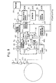
- FIG. 3 of a Sagnac interferometer with closed fiber loop corresponding to the state of the art mentioned shows a light source L, for example a laser, whose parallel light beams are polarized by a polarizer P and split into two light beams via a beam splitter ST2 and in opposite direction are radiated into an interferometer fiber coil FS.
- the fiber spool FS will preferably consist of an optical single-mode fiber.
- the beam splitter ST2 also acts as a mixer for recombining the two light beams after passing through the fiber spool FS.
- the interference signal of the two superimposed light beams After passing through the polarizer P, the interference signal of the two superimposed light beams reaches a via a second beam splitter ST1 and its output branch AUS Photodetector PD, which scans the intensity of the interference image.
- ⁇ 0 the phase difference between the two light beams propagating in opposite directions in the closed fiber coil FS
- the optical Power density at the input of the photodetector PD and the measurement sensitivity is referred to the literature mentioned.
- the sensitivity of the interferometer can be increased by applying a constant, non-reciprocal bias to the two opposing light beams in the fiber coil FS, in such a way that the two opposing light beams (light waves) periodically in the Working point of highest sensitivity of the interferometer can be shifted by angles of (2n + 1) ⁇ ⁇ / 2, where n is an integer.
- the phase modulator PM is initially excited with a signal ⁇ 1 (t), which causes a periodic phase shift of, for example, ⁇ ⁇ / 2, 3 ⁇ / 2, ..., and whose period is 2t0, with t0 the duration of one Light wave in the fiber coil FS is called.
- phase ramp signal the slope of which is proportional to ⁇ / t0, ie to ⁇ , i.e. the non-reciprocal Phase shift.
- the resetting phase ramp signal in the circuit according to FIG. 3 is a sawtooth or step signal, in which the amplitude of a sawtooth or the height of a step is equal to ⁇ , while the duration of a sawtooth or a step has the duration t der or an odd number Corresponds to multiples of t0.
- the function of the circuit according to FIG. 3 is to generate a reciprocal, alternating phase shift optimizing the operating point in time with the frequency f0 and the step-shaped ramp reset signal including a scale factor control is briefly described below:
- the demodulated output signal is fed via an amplifier A, which is generally combined with a filter, as signal VA to an analog / digital converter AD, the digital output signal of which is proportional to the rotation rate and contains sign information with regard to the direction of rotation.
- the signal VAD then passes to a circuit GSC, which essentially contains a digital integrator and delivers a phase control signal VSC, i. H. a composite signal consisting of the digital phase ramp reset signal and the digital phase modulation signal.
- the composite digital signal VSC is then converted into an analog control voltage VC in a digital / analog converter DA and applied as a control voltage to the phase modulator PM via a driver amplifier AP.
- phase modulation signal and the phase ramp reset signal is synchronized and controlled by a central processor CPU via a bidirectional bus BC, which is connected to a quartz-stabilized oscillator OSC, which supplies the frequency f0.
- the central processor CPU Apart from the on a certain angle of rotation, for. B. four arc seconds, related number of bits per word, which correspond to the capacity of an adder contained in the circuit GSC, supplies the latter overflow signals SL. Depending on these overflow signals SL and in accordance with the clock signal of the oscillator OSC, the central processor CPU generates the various control and synchronization signals, and in order to enable a scale factor correction, depending on the overflow condition, the modulation stroke between a "mode A" and a " Mode B "is switched over such that a modulation stroke of, for example, ⁇ ⁇ / 2 applies to mode A and a modulation stroke of ⁇ 3 / 2 ⁇ applies to mode B.
- the detected amplitude differences between the operating states with different modulation strokes are a measure of the scale factor error at the times of the phase ramp signal overflow.
- the known circuit according to FIG. 3 is equipped with a demodulator SFC which detects the amplitude differences of the f0 modulation signal in mode A (phase shift e.g. ⁇ ⁇ / 2) and mode B (phase shift e.g. ⁇ 3 / 2 ⁇ ) detected and this demodulated signal via an integrating amplifier IA as an analog correction signal SIA to a correcting analog input e M of the digital / analog converter DA.
- Switching from "Mode A” to “Mode B” is directly dependent on the ramp value of the resetting sawtooth signal and thus on the angle of rotation of the gyro.
- a ramp run can correspond to an angular increment of, for example, approximately four arc seconds.
- the modulation stroke switchover effectively triggers the gyro bias by tripling the amplitude of the modulation signal and by scattering it into the sensitive signal path of the photodetector signal VD.
- These undesirable stray effects are indicated in the circuit according to FIG. 3 by dashed lines and the coupling factor K.
- this switching of the modulation stroke signal is dependent on the angle of rotation, it leads to an insensitivity range (“lock-in") of the gyro. It can also be shown, as explained below, that this effect leads to a scale factor non-linearity outside the lock-in zone.
- This alternating frequency is proportional to the rotation rate, ie, according to the example explained in the cited US patent specification, a return of 2 ⁇ corresponds to an angular increment of 5 arc seconds; at 1 Hz return frequency, this corresponds to a rotation rate of 5 ° / h.
- EMC e lektro- m agnetic V tolerability
- English EMC measures, e lectro- m agnetic c ompatibility
- shielding indicated in Fig. 3 by shielding the connecting line from the driver amplifier AP to the phase modulator PM
- the signal VSC or VC, VC 'contains the modulation frequency f0 1 ⁇ 2t0, which is generated in the oscillator OSC or via the processor CPU.
- the photodetector signal VD contains the rotation rate information with the same frequency and phase position. This signal is detected in the synchronous demodulator SYNCD.
- the circuit groups that generate the modulation size of the frequency f0 and the circuit parts that carry the rate-sensitive signal of the same frequency are closely related and usually have to be fed from a common power supply device.
- the risk of electromagnetic energy of frequency f0 being scattered into the sensitive signal path (signal VD) is thus obvious.
- Blocking filters for f0 in the signal lines are not possible because the desired signal information is available at precisely this frequency. Undesired interferences can z. B. can only be reduced to a certain extent by shielding the amplifier Aul and the synchronous demodulator SYNCD against the rest of the circuit and by filtering its current supply.
- the spectral component with the frequency f0 in the signal VC or VC ' is generally in the range of a few V.
- the rotation rate signal VD corresponds - depending on the light output, detector sensitivity and gyro scale factor - Voltages in the range of a few nV with a rotation rate of 1 ° / h.
- the closed-loop control loop is used to regulate the ramp slope of the reset signal in proportion to the sum of the true input rotation rate D e and the respective bias B a or B b , depending on whether modulation mode A or B is present.
- the slope during mode B is flatter than in mode A, since B b ⁇ B a is assumed.
- the duty cycle of the modes (T a / T b ) also depends on D e . From this follows the scale factor non-linearity mentioned above.
- the above-mentioned lock-in effect occurs in a rotation rate range in which the sum (D e + B a ) or (D e + B b ) has a different sign for both modes, ie if z.
- the ramp of the reset signal begins, for. B. in mode A with a positive slope, since (D e + B a )> 0 applies as required. If the ramp reaches the (upper) overflow range (overflow signal SL in FIG. 3), the system switches to mode B.
- the control then triggers a negative ramp slope, since (D e + B b ) ⁇ 0 now applies, ie the ramp slope changes its sign and thus leaves the overflow area and mode A applies again.
- This mode A has a positive one again Ramp incline until switching back to mode B, etc.
- the control is thus "trapped", ie the interferometer arrangement becomes insensitive, ie is in the lock-in state.
- the speed of the control determines how quickly the “zigzag ramp” shown in FIG. 2 changes between modes A and B at the overflow limit; this is generally very high.
- the lock-in state applies to an input rotation rate range in which the specified inequalities are fulfilled, ie the lock-in range has a width of
- the respective ramp value means the instantaneous value of the (unmodulated) ramp ⁇ (t).
- This ramp value is proportional to the angle of rotation.
- the ramp slope d ⁇ / dt corresponds to the time derivative of the angle of rotation, i.e. the rate of rotation.
- the problem of the known digital ramp reset method is that the ramp value, ie the value of the angle of rotation, is the criterion for whether operating mode A or B and thus the different biases B a or B b are present and because of B a ⁇ B b influence the ramp slope itself.
- the scale factor error information is, as shown, in the form of an intensity change signal, the frequency of which is proportional to the rotation rate and can change between 0 and approximately 100 kHz if the theoretical duty cycle of the modulation strokes between mode A and mode B is 1: 3.
- the apparent advantage that the information-bearing intensity changes occur more frequently at high rotation rates and thus better scale factor error information is available at high rotation rates is, however, opposed by the fact that the associated signal processing device has to process a comparatively high frequency range.
- the known ramp reset method leads to the absence of the scale factor error information in the region of the rotation rate zero and thus to drift problems.
- the invention is therefore based on the object, the insensitivity range of a fiber optic rotation rate sensor at low rotation rates, i. H. to avoid the "lock-in effect" shown and to obtain easily processed signals for regulating the scale factor.
- An electrical signal which consists of two components, is fed to the phase modulator PM (e.g. circuit according to FIG. 3).
- the first component is a modulation signal which performs a basic control of the interferometer to the reversal points ⁇ ⁇ / 2, ⁇ 3 ⁇ / 2 ... of the interferometer characteristic in a known manner.
- the second component is the reset signal, which is intended to compensate for the Sagnac effect, which is sensitive to the rotation rate, and is provided by the control system, which makes the sum of the measured Sagnac phase and the reset phase zero.
- Both components, and thus also the combined control signal, are time-discrete staircase functions with a cycle time t0, which is equal to the passage time of the light through the fiber coil FS.
- the phase generated by the phase modulator PM is proportional to the difference between two successive values of the discrete-time control signal.
- the voltage range of the control signal for the phase modulator PM can be restricted by adding an appropriate integer multiple of the voltage, which corresponds to the phase 2 ⁇ , to the control signal.
- a modulo operation is used according to the state of the art according to the aforementioned US patent, which limits the control signal to a range corresponding to the interval from 0 to 2 ⁇ . This operation is also called "ramp overflow".
- the light power I measured by the photodetector PD is proportional to the value of the interferometer characteristic currently being driven. Since the slope in the controlled reversal points of the characteristic curve constantly changes its sign due to the modulation process shown above, the demodulator must reverse this effect.
- the modulation method must also serve the further purpose of obtaining the scale factor error signal.
- at least three different reversal points have to be constantly controlled. In the method described in US-A-4 705 399, this is achieved by the automatically occurring ramp overflow, which ensures that, depending on the instantaneous value of the reset signal, different pairs of reversal points, alternately points with positive and negative slope of the Interferometer characteristic, can be controlled.
- the demodulation function must be a periodic function of time, the values with the frequency 1 ⁇ 2t0 Accepts +1 and -1.
- the demodulator input is therefore sensitive to signals which contain components with this frequency. If such a signal is coupled into the demodulator input, the system is simulated to have a rotation rate that is actually not available, ie a bias error occurs.
- the scale factor modulation is generated by the ramp overflows, i. H. if the modulation stroke is dependent on the reset signal, then the bias error is also dependent on the reset signal and the conditions explained above for the occurrence of a look-in zone in the range of low rotation rates are present.
- the technical teaching according to the invention is that the second signal component of the composite modulation signal acting on the phase modulator is formed from the sum of two components, of which the first component consists of alternating values 0 and ⁇ / 2 is formed and the second part is formed from largely correlation-free successive values 0 and ⁇ and that the synchronous demodulator is controlled with the product of four factors, of which the first factor has a constant value of -1, the second factor is -1 if the second component of said second signal component has the value 0, but is +1 if the second component has the value ⁇ , the third factor is -1 if the second component from the last preceding modulation clock has the value 0, but +1 is when the second part from the last previous modulation clock has the value , and the fourth factor is -1 if the first component has the value 0, but is +1 if the first component has the value ⁇ / 2, and that the product of the four factors is corrected for a runtime compensation that
- a modulation signal generator MG generates a modulation signal consisting of bits b0 and b1 with the values ⁇ and ⁇ / 2. This modulation signal is added in the correct position to the reset signal AT 1 supplied by the control device (cf. FIG. 3), with the most significant bit (HSB bit) a0 being assigned the value ⁇ .
- the sum signal PMS controls the phase modulator PM and, in short, the "gyro" via the digital / analog converter DA.
- the HSB bit has the significance ⁇ ; all high-order bits are suppressed, so that a modulo-2 ⁇ operation automatically results.
- the output signal PMS of the digital / analog converter DA passes through the interferometer arrangement or the "gyro path" and reaches the input of the demodulator DEM as a signal e proportional to the received light intensity I.
- the demodulation signal d is supplied by the modulation signal generator MG and reaches the demodulator DEM after a delay compensation T Laufzeit.
- the time-of-flight compensation T0 compensates for the signal propagation times caused by the digital / analog conversion and the filters in the gyro path as well as by the analog / digital conversion, so that the demodulation signal "matches" the received signal e.
- the modulation signal generator contains a random number generator from which the signals b0, b1 and d are derived.
- permanently stored signal patterns can also be used, which are put together in such a way that the required statistical independence is obtained.
- the solution with a random number generator is assumed for the following description.
- the reversal points of the slope to be controlled are odd multiples of ⁇ / 2.
- bit b0 supplied by the modulation signal generator MG is initially arbitrary and can be used as a degree of freedom for the selection of points with a positive or negative slope of the interferometer characteristic.
- This sign signal generated in this way (cf. FIG. 6) is used after the runtime compensation T0 to demodulate the received signal e.
- the structure of the modulation signal generator MG that follows from the above equations is shown in FIG. 6.
- the signal d (n) is statistically independent of s (n), although s (n) is used to generate it. When d (n) is formed, however, s (n) is completely scrambled again by multiplying it by the product r (n) ⁇ r (n-1) formed from random numbers.
- d (n) is statistically independent of all signals occurring in the modulation process and of the reset signal and all signals derived therefrom in the linear sense, so that the conditions set out at the outset are fulfilled.
- FIG. 7 shows a first concrete exemplary embodiment of an interferometer arrangement according to the invention, in which, however, the scale factor control is initially not yet included.
- the assemblies known from FIG. 3 and corresponding to the prior art are not explained again.
- a first signal portion AT 1 of the phase modulator PM signal PMS to be fed to the digital / analog conversion signal from the ramp signal generator RG is fed to a first input of an adder ADD with modulo formation, with the function of the modules IG (integrator) and RG (ramp generator) essentially correspond to the GSC module in FIG. 3.
- the second signal portion AT2 is composed of the signal portions AT21 and AT22 defined in the characterizing part of claim 1 and is provided by the processor CPU.
- the synchronous demodulator SYNCD1 is acted upon in accordance with the second characterizing feature of claim 1 with the delay-corrected signal d (n) derived above.
- FIG. 8 corresponds to that of FIG. 7, but contains the scale factor correction circuit SK defined in claim 2 as an important addition.
- This scale factor correction circuit SK comprises a second synchronous demodulator SYNCD2, the structure of which can correspond to the synchronous demodulator with this function in the circuit according to FIG. 14 of US-A-4 705 399, that is to say essentially consists of a number of differential amplifiers.
- the amplified photodetector signal VD ' is fed to the signal input of the synchronous demodulator SYNCD2.
- the sign-corrected signal d '(n) is fed to the demodulator input via a multiplier MR - corrected for the running time by an adapted value T0' -, the second input of the multiplier MR being acted upon by a subtractor SUB, which continuously records the last output value of the adder ADD via a memory M3, subtracted from the current output value of the adder ADD.
- the output signal VSY2 of the second synchronous demodulator SYNCD2 feeds the input of an integrating amplifier IA, which essentially represents a filter dimensioned according to control engineering aspects and whose output signal SIA corresponds to at least a portion of the time integral of the input signal VSY2.
- the signal SIA is fed as an analog signal to a correction input of the digital / analog converter DA, which delivers as an output variable the signal which acts on the phase modulator PM and which is essentially proportional to the product of the signals PMS (digital) and SIA (analog).
- the amplified photodetector signal VD 'becomes immediate, that is to say before each further one Working process, converted analog / digital and then applies a digital synchronous demodulator SYNCDD1, at whose demodulator input the signal d (n) is present.
- the structure of the arrangement according to FIG. 9 essentially corresponds to that according to FIG. 7.
- FIG. 11 The principle of the synchronous demodulation used in FIG. 9 is illustrated in FIG. 11.
- the illustration in FIG. 11 is immediately understandable for the person skilled in the art and is regarded as part of the description of the invention.
- the representation of FIG. 10 again corresponds to that of FIG. 8, but the scale factor control SK is implemented completely digitally.
- the second synchronous demodulator SYNCDD2 which is supplied with the data signal DMS by the output signal of the analog / digital converter AD, is also implemented as a digital demodulator, which supplies an output-side scale factor correction signal SIAD, which acts on an input of a further multiplier MP, at whose other input the output signal of the adder is ADD, so that the digital / analog converter DA is already supplied with the scale factor-corrected signal.
- a modulation method for the control signal of a phase modulator of a fiber-optic ring interferometer for rotation rate measurement was provided, which avoids the bias errors caused by electromagnetic coupling and the resulting insensitivity ranges, as occur in the prior art, without increasing the necessary control range for the phase modulator.
Abstract
Zur Vermeidung eines Unempfindlichkeitsbereichs und zur Beseitigung von Skalenfaktor-Nichtlinearitäten insbesondere bei kleinen Drehraten wird für einen über einen digitalen Regelkreis phasenrampenrückgestellten faseroptischen Interferometer-Drehratensensor vorgeschlagen, als Demodulationssignal innerhalb des Regelkreises ein statistisch von allen in Betracht kommenden Störsignalen unabhängiges Signal (d) zu verwenden, das aus einem mit einem Zufallszahlengenerator versehenen Modulations-Signalgenerator (MG) stammt, der außerdem statistisch verteilt eine Umschaltung des Phasenmodulatorsignals (PM) auf ganzzahlige Werte von π/2 der Interferometerkennlinie besorgt. <IMAGE>In order to avoid an insensitivity range and to eliminate scale factor non-linearities, especially at low rotation rates, it is proposed for a fiber-optic interferometer rotation rate sensor that is phase-ramp reset via a digital control loop to use a signal (d) that is statistically independent of all interference signals to be considered as a demodulation signal within the control loop. that comes from a modulation signal generator (MG) provided with a random number generator, which also statistically distributes switching of the phase modulator signal (PM) to integer values of π / 2 of the interferometer characteristic. <IMAGE>
Description
Die Erfindung betrifft ein faseroptisches Sagnac-Interferometer zur Drehratenmessung, bei dem zwei aus einer Lichtquelle stammende, durch einen Polarisator polarisierte und durch Strahlteilung erzeugte Lichtstrahlen in entgegengesetzten Richtungen in eine Faserspule eingestrahlt und anschließend wiedervereinigt werden, bei dem das entstehende Interferenzbild nach Durchlauf durch den Polarisator eine Detektoreinrichtung beaufschlagt, deren Ausgangssignal der Lichtintensität des Interferenzbildes entspricht, bei dem die beiden Lichtstrahlen mittels eines in der Faserspule liegenden Phasenmodulators durch ein aus mehreren variablen Anteilen zusammengesetztes, durch eine Modulo-Operation auf einen Wert von 2π begrenztes Signal moduliert werden, wobei ein erster Signalanteil ein durch einen Integrator erzeugtes Rampensignal ist, welches nichtreziproke, inkrementale Phasenverschiebungen der beiden Lichtstrahlen kompensiert, und ein zweiter Signalanteil einen ganzzahligen positiven Wert von π/2 jeweils für eine Zeit t₀ mit t₀ = Laufzeit jedes der Lichtstrahlen durch die Faserspule im Ruhezustand darstellt, bei dem das verstärkte Photodetektorausgangssignal einem mit der Frequenz f₀ = 1/t₀ getakteten ersten Synchrondemodulator zugeführt wird, bei dem das demodulierte Ausgangssignal in einen digitalen Integrator integriert und nach Digital/Analog-/Wandlung als Rampensignal auf den Phasenmodulator zurückgeführt wird, um die nichtreziproken Phasenverschiebungen der Lichtstrahlen zu kompensieren, und bei dem ein Prozessor die Steuer- und Synchronisationssignale für den ersten Synchrondemodulator, einen Analog/Digital-Wandler und den digitalen Integrator liefert.The invention relates to a fiber optic Sagnac interferometer for rotation rate measurement, in which two light rays originating from a light source, polarized by a polarizer and generated by beam splitting are irradiated in opposite directions into a fiber coil and then reunited, in which the resulting interference image after passing through the polarizer a detector device is acted upon, the output signal of which corresponds to the light intensity of the interference image, in which the two light beams are modulated by means of a phase modulator located in the fiber coil by a signal composed of several variable components and limited to a value of 2π by a modulo operation, a first Signal component is a ramp signal generated by an integrator, which compensates for non-reciprocal, incremental phase shifts of the two light beams, and a second signal component represents an integer positive value of π / 2 each for a time t₀ with t₀ = transit time of each of the light beams through the fiber coil in the idle state, in which the amplified photodetector output signal is fed to a first synchronous demodulator clocked with the frequency f₀ = 1 / t₀, in which the demodulated output signal integrated in a digital integrator and after digital / analog / conversion is fed back as a ramp signal to the phase modulator in order to compensate for the non-reciprocal phase shifts of the light beams, and in which a processor controls and synchronizes signals for the first synchronous demodulator, an analog / Digital converter and the digital integrator supplies.
Zum Messen nichtreziproker Phasenverschiebungen in einem faseroptischen Sagnac-Interferometer, auch Ringinterferometer genannt, ist es aus der Druckschrift DE-A1-31 44 162 bekannt, den im Bereich eines Eingangs der Faserspule liegenden Phasenmodulator einerseits mit einem mit der Frequenz f₀ = ½ t₀ umschaltbaren Phasenhub bestimmter Amplitude und andererseits mit einer den Phasenhub ebenfalls verschiebenden Sägezahnspannung zur Nachregelung der nichtreziproken Phasenverschiebungen z. B. aufgrund von Drehraten, zu beaufschlagen, wobei mit t₀ die Laufzeit jedes der Lichtstrahlen durch die Faserspule bezeichnet ist. Die Steigung der kompensierenden oder rückstellenden Sägezahnspannung (Phasenrampe) entspricht der Drehrate, ist also proportional zu Δφ₀/t₀, wobei mitΔφ₀ die nichtreziproke Phasenverschiebung, beispielsweise verursacht durch eine Drehbewegung, bezeichnet ist. In der Praxis jedoch ist das in der genannten DE-Druckschrift beschriebene, sogenannte Phasenrampen-Rückstellverfahren kaum brauchbar, weil für inertiale Drehratenmessungen Genauigkeiten, insbesondere hinsichtlich der umschaltbaren Phasenhübe, der Amplitude bzw. Steigung des Rückstellsignals sowie des Proportionalitäts- oder Skalenfaktors verlangt werden, die sich in analoger Schaltungstechnik nicht gewährleisten lassen.For measuring non-reciprocal phase shifts in a fiber optic Sagnac interferometer, also called a ring interferometer, it is known from the document DE-A1-31 44 162 that the phase modulator located in the area of an input of the fiber coil has a phase shift that can be switched with the frequency f₀ = ½ t₀ certain amplitude and on the other hand with a sawtooth voltage which also shifts the phase shift for readjustment of the non-reciprocal phase shifts z. B. due to yaw rates, with t₀ the transit time of each of the light rays through the fiber spool is designated. The slope of the compensating or resetting sawtooth voltage (phase ramp) corresponds to the yaw rate, is therefore proportional to Δφ₀ / t₀, with Δφ₀ the non-reciprocal phase shift, for example caused by a rotary movement, is designated. In practice, however, the so-called phase ramp reset method described in the above-mentioned DE publication is hardly usable because accuracies are required for inertial rotation rate measurements, in particular with regard to the switchable phase shifts, the amplitude or slope of the reset signal and the proportionality or scale factor, which are required in analog circuit technology cannot be guaranteed.
Mit der US-A-4 705 399 (≙ EP-A1-0 168 292) ist eine bemerkenswerte Weiterentwicklung des in der genannten DE-Druckschrift grundsätzlich beschriebenen Rampenrückstellverfahrens für faseroptische Ringinterferometer bekannt geworden, das bei der Signalauswertung und -aufbereitung vollständig digital arbeitet, so daß sich die erforderliche Signalpräzision insbesondere hinsichtlich der Genauigkeit der umschaltbaren Phasenhübe und des Rampen-Rückstellsignals mit eindeutiger Zuordnung einer automatischen Meßbereichumschaltung sowie einer Korrektur der Skalenfaktoren gewinnen lassen. Anhand der Fig. 3, die - in vereinfachter Darstellung - dem Stand der Technik nach Fig. 14 der genannten Druckschrift US-A-4 705 399 entspricht (vgl. auch H.C. Lefèvre et al. in Integrated Optics: "A practical solution for the Fiber-Optic Gyroscope", SPIE Vol. 719, Fiber Optic Gyros, 1986) - wird zunächst das Funktionsprinzip des digitalen Phasenrampenrückstellverfahrens für faseroptische Drehratensensoren nach dem Stand der Technik erläutert, wobei hinsichtlich der Einzelheiten auf die genannte Literatur verwiesen wird:With US-A-4 705 399 (≙ EP-A1-0 168 292), a remarkable further development of the ramp reset method for fiber-optic ring interferometer, which is basically described in the above-mentioned DE publication, is known, which works completely digitally in the signal evaluation and processing, so that the required signal precision can be obtained in particular with regard to the accuracy of the switchable phase shifts and the ramp reset signal with a clear assignment of an automatic measuring range switchover and a correction of the scale factors. 3, which - in a simplified representation - corresponds to the prior art according to FIG. 14 of the cited document US Pat. No. 4,705,399 (cf. also HC Lefèvre et al. In Integrated Optics: "A practical solution for the Fiber-Optic Gyroscope ", SPIE Vol. 719, Fiber Optic Gyros, 1986) - the functional principle of the digital phase ramp reset method for fiber-optic rotation rate sensors according to the prior art is first explained, reference being made to the literature for details:
Die schematische und vereinfachte Darstellung der Fig. 3 eines dem genannten Stand der Technik entsprechenden Sagnac-Interferometers mit geschlossener Faserschleife zeigt eine Lichtquelle L, beispielsweise einen Laser, dessen parallele Lichtstrahlen durch einen Polarisator P polarisiert und über einen Strahlteiler ST2 in zwei Lichtstrahlen aufgeteilt sowie in entgegengesetzter Richtung in eine Interferometer-Faserspule FS eingestrahlt werden. Die Faserspule FS wird vorzugsweise aus einer optischen Monomodefaser bestehen. Der Strahlteiler ST2 wirkt gleichzeitig als Mischer zur Rekombination der beiden Lichtstrahlen nach Durchlaufen der Faserspule FS. Das Interferenzsignal der beiden überlagerten Lichtstrahlen gelangt nach Durchlaufen des Polarisators P über einen zweiten Strahlteiler ST1 und dessen Ausgangszweig AUS auf einen Photodetektor PD, der die Intensität des Interferenzbildes abtastet. Wird mit Δφ₀ die Phasendifferenz zwischen den beiden sich in entgegengesetzten Richtungen in der geschlossenen Faserspule FS ausbreitenden Lichtstrahlen bezeichnet, so gilt, solange keine nichtreziproken Störungen vorliegen: Δφ₀ = 0. Hinsichtlich des mathematischen Zusammenhangs zwischen der Phasendifferenz Δφ₀ und der Drehrate oder Drehgeschwindigkeit, der optischen Leistungsdichte am Eingang des Photodetektors PD und der Meßempfindlichkeit wird auf die genannte Literatur verwiesen. Dort ist auch beschrieben, wie die Empfindlichkeit des Interferometers durch Beaufschlagung der beiden gegenläufigen Lichtstrahlen in der Faserspule FS durch Einführung eines konstanten, nichtreziproken Bias erhöht werden kann, und zwar so, daß mittels eines Phasenmodulators PM die beiden gegenläufigen Lichtstrahlen (Lichtwellen) periodisch in den Arbeitspunkt höchster Empfindlichkeit des Interferometers um Winkel von (2n + 1)·π/2 verschoben werden, wobei n eine ganze Zahl ist. Zu diesem Zweck wird der Phasenmodulator PM also zunächst mit einem Signal φ₁(t) erregt, das eine periodische Phasenverschiebung von beispielsweise ± π/2, 3π/2 , ..., bewirkt und dessen Periode 2t₀ beträgt, wobei mit t₀ die Laufzeit einer Lichtwelle in der Faserspule FS bezeichnet ist.The schematic and simplified representation of FIG. 3 of a Sagnac interferometer with closed fiber loop corresponding to the state of the art mentioned shows a light source L, for example a laser, whose parallel light beams are polarized by a polarizer P and split into two light beams via a beam splitter ST2 and in opposite direction are radiated into an interferometer fiber coil FS. The fiber spool FS will preferably consist of an optical single-mode fiber. The beam splitter ST2 also acts as a mixer for recombining the two light beams after passing through the fiber spool FS. After passing through the polarizer P, the interference signal of the two superimposed light beams reaches a via a second beam splitter ST1 and its output branch AUS Photodetector PD, which scans the intensity of the interference image. If the phase difference between the two light beams propagating in opposite directions in the closed fiber coil FS is designated with Δφ₀, as long as there are no non-reciprocal disturbances: Δφ₀ = 0. With regard to the mathematical relationship between the phase difference Δφ₀ and the rotation rate or rotational speed, the optical Power density at the input of the photodetector PD and the measurement sensitivity is referred to the literature mentioned. There it is also described how the sensitivity of the interferometer can be increased by applying a constant, non-reciprocal bias to the two opposing light beams in the fiber coil FS, in such a way that the two opposing light beams (light waves) periodically in the Working point of highest sensitivity of the interferometer can be shifted by angles of (2n + 1) · π / 2, where n is an integer. For this purpose, the phase modulator PM is initially excited with a signal φ₁ (t), which causes a periodic phase shift of, for example, ± π / 2, 3π / 2, ..., and whose period is 2t₀, with t₀ the duration of one Light wave in the fiber coil FS is called.
Bei der Schaltung nach Fig. 3 werden, wie in der genannten US-Patentschrift beschrieben, nichtreziproke Phasenverschiebungen durch eine negative Rückkopplung auf den Phasenmodulator PM kompensiert durch ein sogenanntes Phasenrampensignal, dessen Steigung proportional ist zu Δφ/t₀, d. h. zu Δφ, also der nichtreziproken Phasenverschiebung. Das rückstellende Phasenrampensignal ist bei der Schaltung nach Fig. 3 ein Sägezahn- oder Treppenstufensignal, bei dem die Amplitude eines Sägezahns bzw. die Höhe einer Treppenstufe gleich Δφ beträgt, während die Dauer eines Sägezahns oder einer Treppenstufe der Laufzeit t₀ bzw. einem ungeradzahligen Vielfachen von t₀ entspricht.In the circuit according to FIG. 3, as described in the aforementioned US patent, non-reciprocal phase shifts are compensated for by a negative feedback to the phase modulator PM by a so-called phase ramp signal, the slope of which is proportional to Δφ / t₀, ie to Δφ, i.e. the non-reciprocal Phase shift. The resetting phase ramp signal in the circuit according to FIG. 3 is a sawtooth or step signal, in which the amplitude of a sawtooth or the height of a step is equal to Δφ, while the duration of a sawtooth or a step has the duration t der or an odd number Corresponds to multiples of t₀.
Dieses in der Literatur, insbesondere der genannten US-A-4 705 399 beschriebene digitale Phasenrampenprinzip hat gegenüber einer analogen Lösung den entscheidenden Vorteil, daß die Skalenfaktoren des Phasenmodulationssteuersignals und des Phasenrampenrückstellsignals wenigstens im Prinzip korrigiert sind und eine präzise Definition der Sägezahnamplituden des Rückstellsignals gewährleistet ist.This digital phase ramp principle described in the literature, in particular the aforementioned US-A-4 705 399, has the decisive advantage over an analog solution that the scale factors of the phase modulation control signal and the phase ramp reset signal are corrected at least in principle and a precise definition of the sawtooth amplitudes of the reset signal is ensured .
Die Funktion der Schaltung nach Fig. 3 ist zur Erzeugung einer den Arbeitspunkt optimierenden reziproken, alternierenden Phasenverschiebung im Takt der Frequenz f₀ sowie des stufenförmigen Rampenrückstellsignals einschließlich einer Skalenfaktorregelung wird nachfolgend kurz beschrieben:The function of the circuit according to FIG. 3 is to generate a reciprocal, alternating phase shift optimizing the operating point in time with the frequency f₀ and the step-shaped ramp reset signal including a scale factor control is briefly described below:
Das elektrische Signal VD des Photodetektors PD wird über einen Impedanzwandler und Verstärker A₀ angehoben, dessen Ausgangssignal VD' einen Synchrondemodulator SYNCD speist, der auf die Abtastfrequenz f₀ = ½t₀ synchronisiert ist. Das demodulierte Ausgangssignal gelangt über einen in der Regel mit einem Filter kombinierten Verstärker A als Signal VA auf einen Analog/Digital-Wandler AD, dessen digitales Ausgangssignal proportional ist zur Drehrate und eine Vorzeicheninformation hinsichtlich der Drehrichtung enthält. Das Signal VAD gelangt sodann auf eine Schaltung GSC, die im wesentlichen einen digitalen Integrator beinhaltet und ein Phasensteuersignal VSC liefert, d. h. ein zusammengesetztes Signal, bestehend aus dem digitalen Phasenrampen-Rückstellsignal und dem digitalen Phasenmodulationssignal. Das zusammengesetzte Digitalsignal VSC wird anschließend in einem Digital/Analog-Wandler DA in eine analoge Steuerspannung VC gewandelt und über einen Treiberverstärker AP als Steuerspannung auf den Phasenmodulator PM gegeben.The electrical signal VD of the photodetector PD is raised via an impedance converter and amplifier A₀, the output signal VD 'of which feeds a synchronous demodulator SYNCD, which is synchronized with the sampling frequency f₀ = ½t₀. The demodulated output signal is fed via an amplifier A, which is generally combined with a filter, as signal VA to an analog / digital converter AD, the digital output signal of which is proportional to the rotation rate and contains sign information with regard to the direction of rotation. The signal VAD then passes to a circuit GSC, which essentially contains a digital integrator and delivers a phase control signal VSC, i. H. a composite signal consisting of the digital phase ramp reset signal and the digital phase modulation signal. The composite digital signal VSC is then converted into an analog control voltage VC in a digital / analog converter DA and applied as a control voltage to the phase modulator PM via a driver amplifier AP.
Die soweit beschriebene Schaltung zur Erzeugung des Phasenmodulationssignals und des Phasenrampen-Rückstellsignals wird von einem Zentralprozessor CPU über einen bidirektionalen Bus BC synchronisiert und gesteuert, der mit einem quarzstabilisierten Oszillator OSC verbunden ist, der die Frequenz f₀ liefert.The circuit described so far for generating the phase modulation signal and the phase ramp reset signal is synchronized and controlled by a central processor CPU via a bidirectional bus BC, which is connected to a quartz-stabilized oscillator OSC, which supplies the frequency f₀.
Abgesehen von der auf einen bestimmten Drehwinkel, z. B. vier Bogensekunden, bezogenen Anzahl von Bits pro Wort, die der Kapazität eines in der Schaltung GSC enthaltenen Addierers entsprechen, liefert letzterer Überlaufsignale SL. In Abhängigkeit von diesen Überlaufsignalen SL und in Übereinstimmung mit dem Taktsignal des Oszillators OSC generiert der Zentralprozessor CPU die verschiedenen Steuer- und Synchronisationssignale, wobei, um eine Skalenfaktorkorrektur zu ermöglichen, in Abhängigkeit von der Überlaufbedingung der Modulationshub zwischen einem "Modus A" und einem "Modus B" umgeschaltet wird, derart, daß für den Modus A ein Modulationshub von beispielsweise ±π/2 und für den Modus B ein Modulationshub von ±3/2π gilt. Wie in der genannten Literatur beschrieben, sind die detektierten Amplitudendifferenzen zwischen den Betriebszuständen mit unterschiedlichen Modulationshüben ein Maß für den Skalenfaktorfehler zu den Zeitpunkten des Phasenrampensignalüberlaufs. Um diesen Skalenfaktorfehler zu korrigieren, ist die bekannte Schaltung nach Fig. 3 mit einem Demodulator SFC ausgestattet, der die Amplitudenunterschiede des f₀-Modulationssignals im Modus A (Phasenhub z. B. ±π/2) und Modus B (Phasenhub z. B. ±3/2π) erfaßt und dieses demodulierte Signal über einen integrierenden Verstärker IA als analoges Korrektursignal SIA auf einen korrigierenden Analogeingang eM des Digital/Analog-Wandlers DA gibt.Apart from the on a certain angle of rotation, for. B. four arc seconds, related number of bits per word, which correspond to the capacity of an adder contained in the circuit GSC, supplies the latter overflow signals SL. Depending on these overflow signals SL and in accordance with the clock signal of the oscillator OSC, the central processor CPU generates the various control and synchronization signals, and in order to enable a scale factor correction, depending on the overflow condition, the modulation stroke between a "mode A" and a " Mode B "is switched over such that a modulation stroke of, for example, ± π / 2 applies to mode A and a modulation stroke of ± 3 / 2π applies to mode B. As described in the literature mentioned, the detected amplitude differences between the operating states with different modulation strokes are a measure of the scale factor error at the times of the phase ramp signal overflow. In order to correct this scale factor error, the known circuit according to FIG. 3 is equipped with a demodulator SFC which detects the amplitude differences of the f₀ modulation signal in mode A (phase shift e.g. ± π / 2) and mode B (phase shift e.g. ± 3 / 2π) detected and this demodulated signal via an integrating amplifier IA as an analog correction signal SIA to a correcting analog input e M of the digital / analog converter DA.
Dieses soweit anhand der Fig. 3 kurz beschriebene Funktionsprinzip des digitalen Phasenrampen-Rückstellverfahrens für faseroptische Drehratensensoren, bei dem die Steigung der Phasenrampe ein Maß für die rückgestellte Drehrate ist und bei dem in der Rücksprungphase zur Gewinnung eines Korrektursignals für den Skalenfaktor eine Umschaltung des Modulationshubs im Verhältnis 1:3 erfolgt, führt in der Praxis des Betriebs von solchen inertialen Drehratenmeßeinrichtungen zu erheblichen Schwierigkeiten aus folgenden Gründen:This operating principle of the digital phase ramp reset method for fiber optic rotation rate sensors, described briefly with reference to FIG. 3, in which the gradient of the phase ramp is a measure of the reset rotation rate and in the case of a switchover of the modulation stroke in a ratio of 1: 3 in the return phase to obtain a correction signal for the scale factor, the operation of such inertial rotation rate measuring devices leads to considerable difficulties in practice for the following reasons:
Die Umschaltung von "Modus A" auf "Modus B" ist direkt abhängig vom Rampenwert des rückstellenden Sägezahnsignals und damit vom Drehwinkel des Kreisels. Ein Rampendurchlauf kann dabei einem Winkelinkrement von beispielsweise ca. vier Bogensekunden entsprechen. Die Modulationshubumschaltung bewirkt aber über die Verdreifachung der Amplitude des Modulationssignals und über Einstreuungen desselben in den empfindlichen Signalpfad des Photodetektorsignals VD effektiv eine Umschaltung des Kreiselbias. Diese unerwünschten Einstreueffekte sind in der Schaltung nach Fig. 3 durch gestrichelte Linien und den Kopplungsfaktor K angedeutet. Da diese Umschaltung des Modulationshubsignals aber drehwinkelabhängig ist, führt sie zu einem Unempfindlichkeitsbereich ("lock-in") des Kreisels. Es läßt sich auch, wie nachfolgend erläutert, zeigen, daß dieser Effekt außerhalb der Lock-in-Zone zu einer Skalenfaktor-Nichtlinearität führt.Switching from "Mode A" to "Mode B" is directly dependent on the ramp value of the resetting sawtooth signal and thus on the angle of rotation of the gyro. A ramp run can correspond to an angular increment of, for example, approximately four arc seconds. The modulation stroke switchover, however, effectively triggers the gyro bias by tripling the amplitude of the modulation signal and by scattering it into the sensitive signal path of the photodetector signal VD. These undesirable stray effects are indicated in the circuit according to FIG. 3 by dashed lines and the coupling factor K. However, since this switching of the modulation stroke signal is dependent on the angle of rotation, it leads to an insensitivity range ("lock-in") of the gyro. It can also be shown, as explained below, that this effect leads to a scale factor non-linearity outside the lock-in zone.
Wie in Fig. 13 der Druckschrift US-A-4 705 399 gezeigt, ergibt sich bei Vorliegen eines Skalenfaktorfehlers eine unterschiedliche mittlere Intensität I des Photodetektorsignals VD bei Modulationshüben des Modus A bzw. den Modulationshüben des Modus B. Diese Intensitätsdifferenz wird im integrierenden Verstärker IA aufintegriert und liefert das analoge Korrektursignal an einen Eingang eM des Digital/Analog-Wandlers DA. Die Intensitätswechselfrequenz ist gleich der Wechselfrequenz von Modus A auf Modus B und somit gleich der Rampensignal-Rücksprungfrequenz, da die Umschaltung z. B. von Modus A auf Modus B durch Rampenüberlauf (Signal SL eines Addierers) entsteht. Diese Wechselfrequenz ist drehratenproportional, d. h. gemäß dem in der genannten US-Patentschrift erläuterten Beispiel entspricht ein Rücksprung von 2π einem Winkelinkrement von 5 Bogensekunden; bei 1 Hz Rücksprungfrequenz entspricht dies einer Drehrate von 5°/h.As shown in Fig. 13 of the document US-A-4 705 399, there is a different mean intensity I of the photodetector signal VD with modulation strokes of mode A or the modulation strokes of mode B when a scale factor error is present. This intensity difference is in the integrating amplifier IA integrated and delivers the analog correction signal to an input e M of the digital / analog converter DA. The intensity change frequency is equal to the change frequency from mode A to mode B and thus equal to the ramp signal return frequency, since the switch z. B. from mode A to mode B by ramp overflow (Signal SL of an adder) arises. This alternating frequency is proportional to the rotation rate, ie, according to the example explained in the cited US patent specification, a return of 2π corresponds to an angular increment of 5 arc seconds; at 1 Hz return frequency, this corresponds to a rotation rate of 5 ° / h.
Bei kleinen Drehraten kann diese Wechselfrequenz beliebig klein werden, weshalb der integrierende Verstärker IA nur selten die Intensitätsunterschiedinformation erhält. In den dann beliebig langen Intervallen, in denen der Modus nicht wechselt, fehlt dem integrierenden Verstärker IA diese Information, und jeder kleine elektrische Nullpunktfehler an seinem Eingang läßt seine Ausgangsgröße, also das Skalenfaktorkorrektursignal SIA weglaufen (driften). Aus diesem Grund ist der Skalenfaktor bei niedrigen Drehraten anfällig gegen Driften des integrierenden Verstärkers IA. Zwar ist der durch Skalenfaktordriften hervorgerufene prozentuale Drehratenfehler, ausgedrückt in absoluten Drehratenwerten, bei niedrigen Drehraten klein. Problematisch wird aber vor allem ein plötzliches starkes Ansteigen der Drehrate, da dann der Skalenfaktor noch "falsch" ist und somit auch hohe absolute Drehratenfehler entstehen, zumindest so lange, bis der Skalenfaktorregelkreis wieder im eingeschwungenen Zustand ist.At low rotation rates, this alternating frequency can become arbitrarily small, which is why the integrating amplifier IA only rarely receives the intensity difference information. In the then arbitrarily long intervals, in which the mode does not change, the integrating amplifier IA lacks this information, and every small electrical zero point error at its input causes its output variable, i.e. the scale factor correction signal SIA, to drift away. For this reason, the scale factor is susceptible to drifting of the integrating amplifier IA at low rotation rates. The percentage rotation rate error, caused by scale factor drifts, expressed in absolute rotation rate values, is small at low rotation rates. Above all, a sudden sharp increase in the yaw rate becomes problematic, since the scale factor is then still "wrong" and thus also high absolute yaw rate errors occur, at least until the scale factor control loop is in the steady state again.
Es wäre nun naheliegend, die elektromagnetischen Einstreuungen (Störungen mit einem Koppelfaktor K; siehe Fig. 3) durch EMV-Maßnahmen (EMV = elektro-magnetische Verträglichkeit; englisch: EMC measures, electro-magnetic compatibility), also insbesondere durch Abschirmungen (in Fig. 3 angedeutet durch Abschirmung der Verbindungsleitung vom Treiberverstärker AP zum Phasenmodulator PM) und den Einbau von Filtern in Signal- und Spannungszuführleitungen beseitigen oder zumindest vermindern zu wollen. Bei dem bekannten Interferometeraufbau nach Fig. 3 ergibt sich jedoch eine spezielle EMV-Problematik: Das Signal VSC bzw. VC, VC' beinhaltet die Modulationsfrequenz f₀ = ½t₀, die im Oszillator OSC bzw. über den Prozessor CPU erzeugt wird. Das Photodetektorsignal VD beinhaltet aber die Drehrateninformation mit derselben Frequenz und Phasenlage. Dieses Signal wird im Synchrondemodulator SYNCD detektiert. Die Schaltungsgruppen, die die Modulationsgröße der Frequenz f₀ erzeugen, und die Schaltungsteile, die das drehratenempfindliche Signal gleicher Frequenz führen, stehen in engem räumlichem Zusammenhang und müssen in aller Regel aus einer gemeinsamen Stromversorgungseinrichtung gespeist werden. Damit ist die Gefahr der Einstreuung von elektromagnetischer Energie der Frequenz f₀ in den empfindlichen Signalpfad (Signal VD) offenkundig. Sperrfilter für f₀ in den Signalleitungen sind nicht möglich, da die gewünschte Signalinformation bei eben dieser Frequenz vorliegt. Unerwünschte Einstreuungen können also z. B. nur durch Abschirmung des Verstärkers A₀ und des Synchrondemodulators SYNCD gegen den Rest der Schaltung sowie durch Filterung ihrer Stromzuführung in einem gewissen Umfang vermindert werden.It would now be obvious that electromagnetic interferences (disturbances having a coupling coefficient K; see Fig. 3) by EMC measures (EMC = e lektro- m agnetic V tolerability; English: EMC measures, e lectro- m agnetic c ompatibility), ie want to eliminate or at least reduce by shielding (indicated in Fig. 3 by shielding the connecting line from the driver amplifier AP to the phase modulator PM) and the installation of filters in signal and voltage supply lines. 3, however, there is a special one EMC problem: The signal VSC or VC, VC 'contains the modulation frequency f₀ = ½t₀, which is generated in the oscillator OSC or via the processor CPU. However, the photodetector signal VD contains the rotation rate information with the same frequency and phase position. This signal is detected in the synchronous demodulator SYNCD. The circuit groups that generate the modulation size of the frequency f₀ and the circuit parts that carry the rate-sensitive signal of the same frequency are closely related and usually have to be fed from a common power supply device. The risk of electromagnetic energy of frequency f₀ being scattered into the sensitive signal path (signal VD) is thus obvious. Blocking filters for f₀ in the signal lines are not possible because the desired signal information is available at precisely this frequency. Undesired interferences can z. B. can only be reduced to a certain extent by shielding the amplifier Aul and the synchronous demodulator SYNCD against the rest of the circuit and by filtering its current supply.
Ein Zahlenbeispiel für die Einstreuempfindlichkeit wird die besondere Problematik für den Fachmann sofort verdeutlichen: Der Spektralanteil mit der Frequenz f₀ im Signal VC bzw. VC' liegt im allgemeinen im Bereich von einigen V. Im Drehratensignal VD dagegen entsprechen - je nach Lichtleistung, Detektorempfindlichkeit und Kreiselskalenfaktor - Spannungen im Bereich einiger nV einer Drehrate von 1°/h. Bei derart großen Amplitudenunterschieden wird ein unerwünschter Einstreupfad trotz aller möglicher EMV-Maßnahmen unvermeidlich sein, wie dies in Fig. 3 durch den Koppelfaktor K zwischen den Signalen VC, VC' und VD symbolisiert ist; natürlich mit unterschiedlichen Einstreuamplituden und damit unterschiedlichen drehratenäquivalenten Fehlern im Signal VD, und zwar abhängig vom Betriebszustand Modus A bzw. B, da letzterer voraussetzungsgemäß eine dreifach höhere Modulationsamplitude als ersterer aufweist und somit eine stärkere Einstreuung bewirkt. Diese unterschiedlichen Einstreuamplituden führen, auf Drehraten bezogen, zu unterschiedlichen Kreiselnullpunktfehlern, die als Biase Ba bzw. Bb bezeichnet werden, je nach momentanem Modulationszustand Modus A bzw. Modus B.A numerical example of the scattering sensitivity will immediately clarify the particular problem for the person skilled in the art: The spectral component with the frequency f₀ in the signal VC or VC 'is generally in the range of a few V. In contrast, the rotation rate signal VD corresponds - depending on the light output, detector sensitivity and gyro scale factor - Voltages in the range of a few nV with a rotation rate of 1 ° / h. With such large differences in amplitude, an undesirable path of litter will be unavoidable in spite of all possible EMC measures, as symbolized in FIG. 3 by the coupling factor K between the signals VC, VC 'and VD; of course with different litter amplitudes and thus different rotation rate equivalent errors in the signal VD, depending on the operating mode A or B, since the latter is a three times higher one Modulation amplitude as the first and thus causes a greater spread. These different litter amplitudes, based on rotation rates, lead to different gyro zero point errors, which are referred to as Biase B a or B b , depending on the current modulation state mode A or mode B.
Über den geschlossenen Regelkreis wird damit die Rampensteigung des Rückstellsignals proportional zur Summe der wahren Eingangsdrehrate De und des jeweiligen Bias Ba bzw. Bb geregelt, je nachdem, ob Modulationsmodus A bzw. B vorliegt.The closed-loop control loop is used to regulate the ramp slope of the reset signal in proportion to the sum of the true input rotation rate D e and the respective bias B a or B b , depending on whether modulation mode A or B is present.
In Fig. 1 der beigefügten Zeichnungen ist ein Beispiel dargestellt, bei dem De + Ba > 0, De + Bb > 0 und Ba > Bb gilt, also unterschiedliche Biase Ba bzw. Bb vorliegen. Wird De = const. angenommen, so ergeben sich unterschiedliche Rampensteigungen, je nachdem, ob momentan Modus A bzw. Modus B vorliegt, da die Rampensteigung proportional zu De + Ba bzw. proportional zu De + Bb geregelt wird.1 of the accompanying drawings shows an example in which D e + B a > 0, D e + B b > 0 and B a > B b , ie different biases B a and B b are present. If D e = const. Assuming that there are different ramp slopes, depending on whether mode A or mode B is currently present, since the ramp slope is regulated in proportion to D e + B a or in proportion to D e + B b .
In dem in Fig. 1 dargestellten Beispiel ist die Steigung während des Modus B flacher als im Modus A, da Bb < Ba vorausgesetzt wird. Somit wird die Verweildauer tb im Modus B gegenüber der Verweildauer ta im Modus A größer als dies bei modusunabhängigen Biases (Ba = Bb) der Fall wäre. Da jedoch nicht nur Ba, Bb, sondern auch die Eingangsdrehrate De die Rampensteigung in beiden Modi beeinflußt, hängt das Tastverhältnis der Modi (Ta/Tb) auch von De ab. Daraus folgt die oben angesprochene Skalenfaktor-Nichtlinearität.In the example shown in FIG. 1, the slope during mode B is flatter than in mode A, since B b <B a is assumed. Thus, the dwell time t b in mode B becomes longer than the dwell time t a in mode A than would be the case with mode-independent biases (B a = B b ). However, since not only B a , B b , but also the input rotation rate D e influences the ramp gradient in both modes, the duty cycle of the modes (T a / T b ) also depends on D e . From this follows the scale factor non-linearity mentioned above.
Andererseits tritt der oben erwähnte Lock-in-Effekt in einem Drehratenbereich auf, in dem die Summe (De + Ba) bzw. (De + Bb) für beide Modi unterschiedliches Vorzeichen hat, d. h. wenn z. B. gilt (De + Ba) > 0 bzw. (De + Bb) < 0. Dieser für kleine Drehraten durchaus realistische Fall ist in Fig. 2 dargestellt:
Die Rampe des Rückstellsignals (zur besseren Übersichtlichkeit der Darstellung ohne Modulation gezeichnet) beginnt z. B. im Modus A mit positiver Steigung, da (De + Ba) > 0 voraussetzungsgemäß gilt. Erreicht die Rampe den (oberen) Überlaufbereich (Überlaufsignal SL in Fig. 3), so wird auf Modus B gewechselt. Die Regelung steuert dann aber eine negative Rampensteigung an, da jetzt gilt (De + Bb) < 0, d. h. die Rampensteigung wechselt ihr Vorzeichen und verläßt somit den Überlaufbereich und es gilt wieder Modus A. Zu diesem Modus A gehört aber wieder eine positive Rampensteigung, bis wieder nach Modus B umgeschaltet wird usw. Die Regelung hält sich also "gefangen", d. h. die Interferometeranordnung wird unempfindlich, d. h. befindet sich im Lock-in-Zustand. Wie schnell die in Fig. 2 dargestellte "Zick-Zack-Rampe" zwischen den Modi A und B an der Überlaufgrenze wechselt, bestimmt die Schnelligkeit der Regelung; diese liegt im allgemeinen sehr hoch. Der Lock-in-Zustand gilt für einen Eingangsdrehratenbereich, in dem die angegebenen Ungleichungen erfüllt sind, d. h. der Lock-in-Bereich hat also eine Breite von |Ba - Bb|.On the other hand, the above-mentioned lock-in effect occurs in a rotation rate range in which the sum (D e + B a ) or (D e + B b ) has a different sign for both modes, ie if z. For example, (D e + B a )> 0 or (D e + B b ) <0. This is a realistic case for small rotation rates in 2 shown:
The ramp of the reset signal (drawn for clarity of presentation without modulation) begins, for. B. in mode A with a positive slope, since (D e + B a )> 0 applies as required. If the ramp reaches the (upper) overflow range (overflow signal SL in FIG. 3), the system switches to mode B. The control then triggers a negative ramp slope, since (D e + B b ) <0 now applies, ie the ramp slope changes its sign and thus leaves the overflow area and mode A applies again. This mode A has a positive one again Ramp incline until switching back to mode B, etc. The control is thus "trapped", ie the interferometer arrangement becomes insensitive, ie is in the lock-in state. The speed of the control determines how quickly the “zigzag ramp” shown in FIG. 2 changes between modes A and B at the overflow limit; this is generally very high. The lock-in state applies to an input rotation rate range in which the specified inequalities are fulfilled, ie the lock-in range has a width of | B a - B b |.
Bei der soweit gegebenen Beschreibung ist mit dem jeweiligen Rampenwert der Momentanwert der (unmodulierten) Rampe φ(t) gemeint. Dieser Rampenwert ist proportional zum Drehwinkel. Die Rampensteigung dφ/dt entspricht der zeitlichen Ableitung des Drehwinkels, also der Drehrate. Auf den Punkt gebracht, liegt also die Problematik des bekannten digitalen Rampenrückstellverfahrens darin, daß der Rampenwert, d. h. der Wert des Drehwinkels, das Kriterium dafür ist, ob Betriebsmodus A oder B und damit die unterschiedlichen Biases Ba bzw. Bb vorliegen und wegen Ba ≠ Bb die Rampensteigung selbst beeinflussen. Die Skalenfaktorfehlerinformation liegt, wie dargestellt, in Form eines Intensitätsänderungssignals vor, dessen Frequenz drehratenproportional ist und sich zwischen 0 und etwa 100 kHz ändern kann, wenn das theoretische Tastverhältnis der Modulationshübe zwischen Modus A und Modus B 1:3 beträgt. Dem augenscheinlichen Vorteil, daß die informationstragenden Intensitätsänderungen bei hohen Drehraten öfter vorkommen und somit bei hohen Drehraten eine bessere Skalenfaktorfehlerinformation vorliegt, steht aber entgegen, daß die zugehörige Signalverarbeitungseinrichtung einen vergleichsweise hohen Frequenzbereich verarbeiten muß. Andererseits aber führt das bekannte Rampenrückstellverfahren, wie dargestellt, im Bereich der Drehrate Null zum Fehlen der Skalenfaktorfehlerinformation und damit zu Driftproblemen.In the description given so far, the respective ramp value means the instantaneous value of the (unmodulated) ramp φ (t). This ramp value is proportional to the angle of rotation. The ramp slope dφ / dt corresponds to the time derivative of the angle of rotation, i.e. the rate of rotation. In a nutshell, the problem of the known digital ramp reset method is that the ramp value, ie the value of the angle of rotation, is the criterion for whether operating mode A or B and thus the different biases B a or B b are present and because of B a ≠ B b influence the ramp slope itself. The scale factor error information is, as shown, in the form of an intensity change signal, the frequency of which is proportional to the rotation rate and can change between 0 and approximately 100 kHz if the theoretical duty cycle of the modulation strokes between mode A and mode B is 1: 3. The apparent advantage that the information-bearing intensity changes occur more frequently at high rotation rates and thus better scale factor error information is available at high rotation rates is, however, opposed by the fact that the associated signal processing device has to process a comparatively high frequency range. On the other hand, however, the known ramp reset method, as shown, leads to the absence of the scale factor error information in the region of the rotation rate zero and thus to drift problems.
Der Erfindung liegt damit die Aufgabe zugrunde, den Unempfindlichkeitsbereich eines faseroptischen Drehratensensors bei kleinen Drehraten, d. h. den dargestellten "Lock-in-Effekt", zu vermeiden und gut zu verarbeitende Signale zur Regelung des Skalenfaktors zu gewinnen.The invention is therefore based on the object, the insensitivity range of a fiber optic rotation rate sensor at low rotation rates, i. H. to avoid the "lock-in effect" shown and to obtain easily processed signals for regulating the scale factor.
Als Vorstufe zur Lösung der gestellten Aufgabe und um das Verständnis der Erfindung zu erleichtern, seien zunächst noch einmal die bei den bekannten, in der oben erwähnten Literatur beschriebenen Verfahren angewendeten Signalverarbeitungsprozesse betrachtet:
Dem Phasenmodulator PM (z. B. Schaltung nach Fig. 3) wird ein elektrisches Signal zugeführt, das aus zwei Komponenten besteht. Die erste Komponente ist ein Modulationssignal, das in bekannter Weise eine Grundaussteuerung des Interferometers zu den Umkehrpunkten ±π/2, ±3π/2 ... der Interferometerkennlinie vornimmt. Die zweite Komponente ist das Rückstellsignal, welches den drehratenempfindlichen Sagnac-Effekt kompensieren soll und von dem Regelsystem bereitgestellt wird, das die Summe aus gemessener Sagnac-Phase und Rückstellphase zu Null macht. Beide Komponenten, und damit auch das zusammengesetzte Ansteuersignal, sind zeitdiskrete Treppenfunktionen mit einer Taktzeit t₀, die gleich der Durchlaufzeit des Lichts durch die Faserspule FS ist. Die durch den Phasenmodulator PM erzeugte Phase ist proportional zur Differenz zweier aufeinanderfolgender Werte des zeitdiskreten Ansteuersignals.As a preliminary step to solving the problem and to facilitate understanding of the invention, the signal processing processes used in the known methods described in the above-mentioned literature are considered again:
An electrical signal, which consists of two components, is fed to the phase modulator PM (e.g. circuit according to FIG. 3). The first component is a modulation signal which performs a basic control of the interferometer to the reversal points ± π / 2, ± 3π / 2 ... of the interferometer characteristic in a known manner. The second component is the reset signal, which is intended to compensate for the Sagnac effect, which is sensitive to the rotation rate, and is provided by the control system, which makes the sum of the measured Sagnac phase and the reset phase zero. Both components, and thus also the combined control signal, are time-discrete staircase functions with a cycle time t₀, which is equal to the passage time of the light through the fiber coil FS. The The phase generated by the phase modulator PM is proportional to the difference between two successive values of the discrete-time control signal.
Da die Interferometerkennlinie (Fig. 4) eine in 2π periodische Funktion ist, kann der Spannungsbereich des Ansteuersignals für den Phasenmodulator PM eingeschränkt werden, indem ein passendes ganzzahliges Vielfaches der Spannung, die der Phase 2π entspricht, zum Ansteuersignal hinzuaddiert wird. Hierzu wird gemäß dem Stand der Technik nach der genannten US-Patentschrift eine Modulo-Operation eingesetzt, die das Ansteuersignal auf einen dem Intervall von 0 bis 2π entsprechenden Bereich eingrenzt. Diese Operation wird auch als "Rampenüberlauf" bezeichnet. Die durch den Photodetektor PD gemessene Lichtleistung I ist dem Wert der momentan angesteuerten Interferometerkennlinie proportional. Da die Steigung in den angesteuerten Umkehrpunkten der Kennlinie aufgrund des oben dargestellten Modulationsprozesses ständig ihr Vorzeichen ändert, muß der Demodulator diesen Effekt wieder rückgängig machen.Since the interferometer characteristic curve (FIG. 4) is a periodic function in 2π, the voltage range of the control signal for the phase modulator PM can be restricted by adding an appropriate integer multiple of the voltage, which corresponds to the phase 2π, to the control signal. For this purpose, a modulo operation is used according to the state of the art according to the aforementioned US patent, which limits the control signal to a range corresponding to the interval from 0 to 2π. This operation is also called "ramp overflow". The light power I measured by the photodetector PD is proportional to the value of the interferometer characteristic currently being driven. Since the slope in the controlled reversal points of the characteristic curve constantly changes its sign due to the modulation process shown above, the demodulator must reverse this effect.
Neben dem oben genannten Zweck, nämlich durch Ansteuerung der Umkehrpunkte der Interferometerkennlinie ein drehratenempfindliches Signal zu gewinnen, muß das Modulationsverfahren noch den weiteren Zweck der Gewinnung des Skalenfaktorfehlersignals erfüllen. Um diese zusätzliche Information zu erhalten, müssen ständig mindestens drei verschiedene Umkehrpunkte angesteuert werden. Bei dem in der Druckschrift US-A-4 705 399 beschriebenen Verfahren wird dies durch den automatisch auftretenden Rampenüberlauf erreicht, der dafür sorgt, daß, abhängig vom Momentanwert des Rückstellsignals, verschiedene Paare von Umkehrpunkten, und zwar abwechselnd Punkte mit positiver und negativer Steigung der Interferometerkennlinie, angesteuert werden. Demzufolge muß die Demodulationsfunktion eine periodische Funktion der Zeit sein, die mit der Frequenz ½t₀ die Werte +1 und -1 annimmt. Damit aber ist der Demodulatoreingang aus den oben erläuterten Gründen empfindlich gegen Signale, die Anteile mit dieser Frequenz enthalten. Wird ein derartiges Signal in den Demodulatoreingang eingekoppelt, so wird dem System eine Drehrate vorgetäuscht, die tatsächlich nicht vorhanden ist, d. h. es entsteht ein Bias-Fehler.In addition to the above-mentioned purpose, namely to obtain a rate-sensitive signal by controlling the reversal points of the interferometer characteristic, the modulation method must also serve the further purpose of obtaining the scale factor error signal. In order to obtain this additional information, at least three different reversal points have to be constantly controlled. In the method described in US-A-4 705 399, this is achieved by the automatically occurring ramp overflow, which ensures that, depending on the instantaneous value of the reset signal, different pairs of reversal points, alternately points with positive and negative slope of the Interferometer characteristic, can be controlled. Accordingly, the demodulation function must be a periodic function of time, the values with the frequency ½t₀ Accepts +1 and -1. However, for the reasons explained above, the demodulator input is therefore sensitive to signals which contain components with this frequency. If such a signal is coupled into the demodulator input, the system is simulated to have a rotation rate that is actually not available, ie a bias error occurs.
Wenn, wie in der genannten US-Patentschrift erläutert, die Skalenfaktormodulation durch die Rampenüberläufe erzeugt wird, d. h. wenn der Modulationshub vom Rückstellsignal abhängig ist, dann ist auch der Bias-Fehler vom Rückstellsignal abhängig und die oben erläuterten Bedingungen für das Auftreten einer Look-in-Zone im Bereich geringer Drehraten liegen vor.If, as explained in said U.S. patent, the scale factor modulation is generated by the ramp overflows, i. H. if the modulation stroke is dependent on the reset signal, then the bias error is also dependent on the reset signal and the conditions explained above for the occurrence of a look-in zone in the range of low rotation rates are present.
Mit der europäischen Patentanmeldung Nr. 90 100 103.2 wurde bereits vorgeschlagen, diesen Effekt dadurch zu beseitigen, daß die Skalenfaktormodulation unabhängig vom Rückstellsignal erzeugt wird. Dann verbleibt zwar ein Bias-Fehler, der jedoch durch ein geeignetes Taktverhältnis für die Skalenfaktormodulation im Mittel zu Null gemacht werden kann. Die vom Bias-Fehler hervorgerufene Unempfindlichkeitszone tritt nicht mehr auf. Die bereits vorgeschlagene Lösung des aufgezeigten Problems bedingt jedoch einen höheren Aussteuerbereich für den Phasenmodulator PM, nämlich von 7π/2 gegenüber 2π bei den anderen bekannten Verfahren, z. B. nach der erwähnten US-Patentschrift.With European patent application No. 90 100 103.2 it has already been proposed to eliminate this effect in that the scale factor modulation is generated independently of the reset signal. A bias error then remains, but this can be made zero on average by using a suitable clock ratio for the scale factor modulation. The insensitivity zone caused by the bias error no longer occurs. The solution to the problem already suggested, however, requires a higher modulation range for the phase modulator PM, namely of 7π / 2 compared to 2π in the other known methods, eg. B. according to the mentioned US patent.
Als Grundlage der Erfindung wurde erkannt, daß das Auftreten von Bias-Fehlern, die durch Einkopplung von Störsignalen in den Demodulatoreingang entstehen, durch die Verwendung eines Demodulationssignals unterdrückt werden kann, das statistisch unabhängig ist von allen als Ursache von Störsignalen in Betracht kommenden Signalquellen.As the basis of the invention, it was recognized that the occurrence of bias errors, which arise from the coupling of interference signals into the demodulator input, can be suppressed by using a demodulation signal which is statistically independent of all signal sources which are considered to be the cause of interference signals.
Auf der Grundlage und unter Verwendung eines faseroptischen Sagnac-Interferometers gemäß dem eingangs angegebenen Oberbegriff des Patentanspruchs 1 besteht die erfindungsgemäße technische Lehre darin, daß der zweite Signalanteil des den Phasenmodulator beaufschlagenden zusammengesetzten Modulationssignals aus der Summe von zwei Anteilen gebildet wird, von denen der erste Anteil aus wechselweise aufeinanderfolgenden Werten 0 und π/2 gebildet ist und der zweite Anteil aus weitgehend korrelationsfrei aufeinanderfolgenden Werten 0 und π gebildet ist und daß der Synchrondemodulator mit dem Produkt aus vier Faktoren angesteuert wird, von denen der erste Faktor konstant den Wert -1 hat, der zweite Faktor -1 ist, wenn der zweite Anteil des genannten zweiten Signalanteils den Wert 0 hat, jedoch +1 ist, wenn der zweite Anteil den Wert π hat, der dritte Faktor -1 ist, wenn der zweite Anteil aus dem letzten vorhergehenden Modulationstakt den Wert 0 hat, jedoch +1 ist, wenn der zweite Anteil aus dem letzten vorhergehenden Modulationstakt den Wert π hatte, und der vierte Faktor dann -1 ist, wenn der erste Anteil den Wert 0 hat, jedoch +1 ist, wenn der erste Anteil den Wert π/2 hat, und daß das Produkt der vier Faktoren um einen Laufzeitausgleich korrigiert wird, der der Zeit t₀ sowie der Prozeßzeit für die Summation zur Gewinnung des zweiten Signalanteils, zur Zusammensetzung des ersten und zweiten Signalanteils zum Ansteuersignal für den Phasenmodulator und der Digital/Analogwandlung entspricht.Based on and using a fiber optic Sagnac interferometer according to the preamble of claim 1, the technical teaching according to the invention is that the second signal component of the composite modulation signal acting on the phase modulator is formed from the sum of two components, of which the first component consists of alternating values 0 and π / 2 is formed and the second part is formed from largely correlation-free successive values 0 and π and that the synchronous demodulator is controlled with the product of four factors, of which the first factor has a constant value of -1, the second factor is -1 if the second component of said second signal component has the value 0, but is +1 if the second component has the value π, the third factor is -1 if the second component from the last preceding modulation clock has the value 0, but +1 is when the second part from the last previous modulation clock has the value , and the fourth factor is -1 if the first component has the value 0, but is +1 if the first component has the value π / 2, and that the product of the four factors is corrected for a runtime compensation that corresponds to the time t₀ and the process time for the summation for obtaining the second signal component, for the composition of the first and second signal components for the control signal for the phase modulator and the digital / analog conversion.
Die Erfindung und vorteilhafte Einzelheiten werden nachfolgend unter Bezug auf die Zeichnung zunächst an einer grundsätzlichen und sodann anhand verschiedener abgewandelter Ausführungsformen näher erläutert. Es zeigen:
- Fig. 1
- die bereits erläuterte, beim Stand der Technik von der Modulationshubänderung, also dem Betriebsmodus, abhängige Änderung der Rampensteigung des Rückstellsignals;
- Fig. 2
- die ebenfalls bereits erläuterte Entstehung des Lock-in-Effekts bei kleinen Drehraten;
- Fig. 3
- eine ebenfalls bereits erläuterte, dem Stand der Technik entsprechende Anordnung eines faseroptischen Interferometers mit digitaler Verarbeitung des Drehratensignals und Erzeugung der Modulationshubsignale und des Rampenrückstellsignals;
- Fig. 4
- die Interferometerkennlinie mit eingetragenen Umkehrpunkten;
- Fig. 5
- eine schematische, jedoch prinzipielle, Blockschaltbildanordnung zur Erzeugung von Modulations- und Demodulationssignalen gemäß dem Grundprinzip der Erfindung;
- Fig. 6
- den Aufbau eines Modulationssignalgenerators gemäß der Erfindung;
- Fig. 7
- eine dem Blockschaltbild der Fig. 3 (Stand der Technik) entsprechende Anwendung der Erfindung;
- Fig. 8
- einen der Fig. 7 entsprechenden Interferometeraufbau, jedoch mit erfindungsgemäß ergänzter Skalenfaktorkorrekturschaltung;
- Fig. 9
- eine gegenüber Fig. 7 abgewandelte Blockschaltbildanordnung, bei der (vgl. Patentanspruch 3) die Analog/Digitalwandlung des Interferometersignals unmittelbar nach einer Signalverstärkung erfolgt und dementsprechend eine digitale Synchrondemodulation angewendet wird;
- Fig. 10
- einen der Fig. 9 entsprechenden Interferometeraufbau, jedoch wiederum (entsprechend Fig. 8) mit ergänzter Skalenfaktorkorrekturschaltung;
- Fig. 11
- die Prinzipanordnung für eine digitale Synchrondemodulation; und
- Fig. 12
- einen prinzipiellen Blockschaltbildaufbau, bei dem der gesamte Verarbeitungsprozeß zur Bereitstellung des Ansteuersignals für den Phasenmodulator in einer zentralen Recheneinheit abläuft.
- Fig. 1
- the change in the ramp gradient of the reset signal which has already been explained and which is dependent on the modulation stroke change, that is to say the operating mode, in the prior art;
- Fig. 2
- the development of the lock-in effect at low rotation rates, which has also already been explained;
- Fig. 3
- an arrangement of a fiber-optic interferometer, which has also already been explained and corresponds to the prior art, with digital processing of the rotation rate signal and generation of the modulation stroke signals and the ramp reset signal;
- Fig. 4
- the interferometer characteristic with entered reversal points;
- Fig. 5
- a schematic, but basic, block diagram arrangement for generating modulation and demodulation signals according to the basic principle of the invention;
- Fig. 6
- the construction of a modulation signal generator according to the invention;
- Fig. 7
- an application of the invention corresponding to the block diagram of Figure 3 (prior art).
- Fig. 8
- an interferometer structure corresponding to FIG. 7, but with a scale factor correction circuit added according to the invention;
- Fig. 9
- a block diagram arrangement modified compared to FIG. 7, in which (cf. claim 3) the analog / digital conversion of the interferometer signal takes place immediately after signal amplification and accordingly a digital synchronous demodulation is used;
- Fig. 10
- one corresponding to FIG. 9, but again (according to FIG. 8) with an additional one Scale factor correction circuit;
- Fig. 11
- the basic arrangement for digital synchronous demodulation; and
- Fig. 12
- a basic block diagram structure, in which the entire processing process for providing the control signal for the phase modulator runs in a central processing unit.
Fig. 5 zeigt in prinzipieller Anordnung den für die Erfindung wesentlichen Teil einer Ringinterferometeranordnung, nämlich diejenigen Teile und Baugruppen, die für die Modulation und Demodulation wichtig sind. Ein Modulations-Signalgenerator MG erzeugt ein Modulationssignal, bestehend aus Bits b0 und b1 mit den Wertigkeiten π bzw. π/2. Dieses Modulationssignal wird stellenwertrichtig zu dem von der Regeleinrichtung (vgl. Fig. 3) gelieferten Rückstellsignal AT₁ addiert, wobei dem höchstwertigen Bit (HSB-Bit) a0 die Wertigkeit π zugeordnet ist. Das Summensignal PMS steuert über den Digital/Analog-Wandler DA den Phasenmodulator PM und damit kurz gesagt, den "Kreisel" an. Das HSB-Bit hat, wie erwähnt, die Wertigkeit π; alle höherwertigen Bits werden unterdrückt, so daß sich automatisch eine Modulo-2π-Operation ergibt. Das Ausgangssignal PMS des Digital/Analog-Wandlers DA durchläuft die Interferometeranordnung oder den "Kreiselpfad" und gelangt als ein der empfangenen Lichtintensität I proportionales Signal e auf den Eingang des Demodulators DEM. Das Demodulationssignal d liefert der Modulations-Signalgenerator MG und gelangt nach einem Laufzeitausgleich T₀ an den Demodulator DEM. Der Laufzeitausgleich T₀ kompensiert die durch die Digital/Analog-Wandlung und die im Kreiselpfad liegenden Filter sowie durch die Analog/Digital-Wandlung hervorgerufenen Signallaufzeiten, so daß das Demodulationssignal zum empfangenen Signal e "paßt".5 shows in a basic arrangement the part of a ring interferometer arrangement that is essential for the invention, namely those parts and assemblies that are important for the modulation and demodulation. A modulation signal generator MG generates a modulation signal consisting of bits b0 and b1 with the values π and π / 2. This modulation signal is added in the correct position to the reset signal AT 1 supplied by the control device (cf. FIG. 3), with the most significant bit (HSB bit) a0 being assigned the value π. The sum signal PMS controls the phase modulator PM and, in short, the "gyro" via the digital / analog converter DA. As mentioned, the HSB bit has the significance π; all high-order bits are suppressed, so that a modulo-2π operation automatically results. The output signal PMS of the digital / analog converter DA passes through the interferometer arrangement or the "gyro path" and reaches the input of the demodulator DEM as a signal e proportional to the received light intensity I. The demodulation signal d is supplied by the modulation signal generator MG and reaches the demodulator DEM after a delay compensation T Laufzeit. The time-of-flight compensation T₀ compensates for the signal propagation times caused by the digital / analog conversion and the filters in the gyro path as well as by the analog / digital conversion, so that the demodulation signal "matches" the received signal e.
Um die erwähnte statistische Unabhängigkeit des Demodulationssignals d von allen anderen als Störquellen in Betracht kommenden Signalen zu garantieren, enthält der Modulations-Signalgenerator einen Zufallszahlengenerator, aus dem die Signale b0, b1 und d abgeleitet werden. Alternativ können auch fest abgespeicherte Signalmuster verwendet werden, die so zusammengesetzt werden, daß sich die geforderte statistische Unabhängigkeit ergibt. Für die folgende Beschreibung wird von der Lösung mit einem Zufallszahlengenerator ausgegangen.In order to guarantee the aforementioned statistical independence of the demodulation signal d from all other signals that are considered as sources of interference, the modulation signal generator contains a random number generator from which the signals b0, b1 and d are derived. Alternatively, permanently stored signal patterns can also be used, which are put together in such a way that the required statistical independence is obtained. The solution with a random number generator is assumed for the following description.
Wie sich aus der Interferometerkennlinie gemäß Fig. 4 ablesen läßt, liegen die anzusteuernden Umkehrpunkte der Steigung bei ungeradzahligen Vielfachen von π/2. Sofern keine Drehrate vorliegt (Ruhezustand), besteht die Interferometerphase aus der Differenz der momentanen Modulatorphase p(n) und der zeitlich vorangegangenen Modulatorphase p(n-1). Damit diese Differenz stets ein ungeradzahliges Vielfaches von π/2 ist, muß p(n) abwechselnd ein geradzahliges bzw. ungeradzahliges Vielfaches von π/2 sein, d. h., das vom Modulations-Signalgenerator MG gelieferte Bit b1 mit der Wertigkeit π/2 muß ständig oszillieren:
![]()
As can be seen from the interferometer characteristic curve according to FIG. 4, the reversal points of the slope to be controlled are odd multiples of π / 2. If there is no rotation rate (idle state), the interferometer phase consists of the difference between the current modulator phase p (n) and the previous modulator phase p (n-1). So that this difference is always an odd multiple of π / 2, p (n) must alternately be an even or odd multiple of π / 2, ie the bit b1 supplied by the modulation signal generator MG with the value π / 2 must always be oscillate:
![]()
Dieses Bit b1(n) wird erzeugt aus einem internen Signal s(n)
![]()
![]()
This bit b1 (n) is generated from an internal signal s (n)
![]()
![]()
Das vom Modulations-Signalgenerator MG gelieferte Bit b0 ist zunächst beliebig und kann als Freiheitsgrad für die Auswahl von Punkten mit positiver oder negativer Steigung der Interferometerkennlinie verwendet werden. Bei der hier vorgeschlagenen Lösung wird das Bit b0 aus der von einem Zufallszahlengenerator gelieferten Zahlenfolge R(n) abgeleitet, die gleich verteilt und statistisch unabhängig den Werten -1 oder 1 entspricht. Das Bit b0 ergibt sich hieraus durch
![]()
The bit b0 supplied by the modulation signal generator MG is initially arbitrary and can be used as a degree of freedom for the selection of points with a positive or negative slope of the interferometer characteristic. In the solution proposed here, bit b0 is made up of that of a Random number generator supplied number sequence R (n) derived, which is equally distributed and statistically independent of the values -1 or 1. Bit b0 results from this
![]()
Das Vorzeichen des jeweils angesprungenen Punkts der Interferometerkennlinie ergibt sich somit aus
![]()
The sign of the point of the interferometer characteristic curve that has jumped to is obtained from
![]()
Dieses so erzeugte Vorzeichensignal (vgl. Fig. 6) wird, nachdem es den Laufzeitausgleich T₀ passiert hat, zur Demodulation des empfangenen Signals e verwendet.This sign signal generated in this way (cf. FIG. 6) is used after the runtime compensation T₀ to demodulate the received signal e.
Der aus den obigen Gleichungen folgende Aufbau des Modulations-Signalgenerators MG geht aus Fig. 6 hervor. Das Signal d(n) ist von s(n) statistisch unabhängig, obwohl s(n) zu seiner Erzeugung herangezogen wird. Bei der Bildung von d(n) wird aber s(n) durch die Multiplikation mit dem aus Zufallszahlen gebildeten Produkt r(n)·r(n-1) wieder vollständig verwürfelt. Das Demodulationssignal d(n) ist aber auch von r(n) statistisch unabhängig, weil t(n)=r(n)·r(n-1) von r(n) statistisch unabhängig ist, d. h., daß die kreuzkorrelierte Crt(i) zwischen r(n) und t(n) identisch gleich Null ist. Dieses Ergebnis ist offensichtlich für i ungleich 0 und 1, da dann die um 0 oder 1 Positionen gegeneinander verschobenen Glieder der Folgen r(n) und t(n) keine gemeinsame Information mehr tragen. Für i=0 oder 1 ergibt sich, daß die Kreuzkorrelierte von Crt(0) bzw. Crt(1) dem Mittelwert der Folge r(n) entspricht, welcher voraussetzungsgemäß gleich 0 ist.The structure of the modulation signal generator MG that follows from the above equations is shown in FIG. 6. The signal d (n) is statistically independent of s (n), although s (n) is used to generate it. When d (n) is formed, however, s (n) is completely scrambled again by multiplying it by the product r (n) · r (n-1) formed from random numbers. The demodulation signal d (n) is also statistically independent of r (n) because t (n) = r (n) · r (n-1) is statistically independent of r (n), i.e. that is, the cross-correlated Crt (i) between r (n) and t (n) is identically zero. This result is obviously not equal to 0 and 1 for i, since then the elements of the sequences r (n) and t (n) shifted by 0 or 1 positions relative to one another no longer carry any common information. For i = 0 or 1, it follows that the cross-correlation of Crt (0) or Crt (1) corresponds to the mean value of the sequence r (n), which is assumed to be 0.
Die Korrelation zwischen r(n) und t(n) läßt sich wie folgt darstellen:
Es gilt t(n) = r(n)·r(n-1)
Für i ≠ 0 und i ≠ 1:
Crt(i) = 0 evident!
d. h.:
Crt(i) = 0 für alle iThe correlation between r (n) and t (n) can be represented as follows:
The following applies: t (n) = r (n) r (n-1)
For i ≠ 0 and i ≠ 1:
Crt (i) = 0 evident!
ie:
Crt (i) = 0 for all i
Daraus ergibt sich, daß d(n) von allen beim Modulationsprozeß auftretenden Signalen sowie vom Rückstellsignal und allen aus diesen abgeleiteten Signalen im linearen Sinn statistisch unabhängig ist, so daß die eingangs aufgestellten Voraussetzungen erfüllt sind.It follows from this that d (n) is statistically independent of all signals occurring in the modulation process and of the reset signal and all signals derived therefrom in the linear sense, so that the conditions set out at the outset are fulfilled.
Die Fig. 7 zeigt ein erstes konkretes Ausführungsbeispiel einer erfindungsgemäßen Interferometeranordnung, bei der jedoch zunächst die Skalenfaktorregelung noch nicht enthalten ist. Die aus der Fig. 3 bekannten und dem Stand der Technik entsprechenden Baugruppen werden nicht erneut erläutert.FIG. 7 shows a first concrete exemplary embodiment of an interferometer arrangement according to the invention, in which, however, the scale factor control is initially not yet included. The assemblies known from FIG. 3 and corresponding to the prior art are not explained again.
Wie dargestellt, wird (vgl. auch Patentanspruch 1) ein erster Signalanteil AT₁ des nach Digital/Analog-Wandlung dem Phasenmodulator PM zuzuführenden Signals PMS vom Rampen-Signalgenerator RG an einen ersten Eingang eines Addierers ADD mit Modulobildung zugeführt, wobei in ihrer Funktion die Baugruppen IG (Integrator) und RG (Rampengenerator) im wesentlichen der Baugruppe GSC in Fig. 3 entsprechen. Der zweite Signalanteil AT₂ setzt sich aus den im Kennzeichen des Anspruchs 1 definierten Signalanteilen AT₂₁ und AT₂₂ zusammen und wird vom Prozessor CPU bereitgestellt.As shown, a first signal portion AT 1 of the phase modulator PM signal PMS to be fed to the digital / analog conversion signal from the ramp signal generator RG is fed to a first input of an adder ADD with modulo formation, with the function of the modules IG (integrator) and RG (ramp generator) essentially correspond to the GSC module in FIG. 3. The second signal portion AT₂ is composed of the signal portions AT₂₁ and AT₂₂ defined in the characterizing part of
Der Synchrondemodulator SYNCD1 wird entsprechend dem zweiten kennzeichnenden Merkmal des Anspruchs 1 mit dem oben abgeleiteten laufzeitkorrigierten Signal d(n) beaufschlagt.The synchronous demodulator SYNCD1 is acted upon in accordance with the second characterizing feature of
Die Darstellung der Fig. 8 entspricht derjenigen der Fig. 7, enthält jedoch als wichtige Ergänzung die im Patentanspruch 2 definierte Skalenfaktorkorrekturschaltung SK. Diese Skalenfaktorkorrekturschaltung SK umfaßt einen zweiten Synchrondemodulator SYNCD2, dessen Aufbau dem Synchrondemodulator mit dieser Funktion in der Schaltung nach Fig. 14 von US-A-4 705 399 entsprechen kann, also im wesentlichen aus einer Anzahl von Differenzverstärkern besteht. Dem Signaleingang des Synchrondemodulators SYNCD2 wird das verstärkte Photodetektorsignal VD' zugeführt. Dem Demodulatoreingang wird das vorzeichenkorrigierte Signal d'(n) über einen Multiplizierer MR - laufzeitkorrigiert um einen angepaßten Wert T₀' - zugeführt, wobei der zweite Eingang des Multiplizierers MR von einem Subtrahierer SUB beaufschlagt ist, welcher fortlaufend den letzten Ausgangswert des Addierers ADD, erfaßt über einen Speicher M3, vom aktuellen Ausgangswert des Addierers ADD subtrahiert. Das Ausgangssignal VSY2 des zweiten Synchrondemodulators SYNCD2 speist den Eingang eines integrierenden Verstärkers IA, der im wesentlichen ein nach regelungstechnischen Gesichtspunkten dimensioniertes Filter darstellt und dessen Ausgangssignal SIA zumindest einem Anteil des zeitigen Integrals des Eingangssignals VSY2 entspricht. Das Signal SIA wird als Analogsignal einem Korrektureingang des Digital/Analog-Wandlers DA zugeführt, der als Ausgangsgröße das den Phasenmodulator PM beaufschlagende Signal liefert, das im wesentlichen proportional ist zum Produkt der Signale PMS (digital) und SIA (analog).The representation of FIG. 8 corresponds to that of FIG. 7, but contains the scale factor correction circuit SK defined in
Bei der Schaltungsanordnung nach Fig. 9, deren Darstellungsweise jener der Fig. 7 entspricht, wird das verstärkte Photodetektorsignal VD' unmittelbar, also vor jedem weiteren Arbeitsprozeß, analog/digital-gewandelt und beaufschlagt dann einen digitalen Synchrondemodulator SYNCDD1, an dessen Demodulatoreingang das Signal d(n) anliegt. Ansonsten entspricht der Aufbau der Anordnung nach Fig. 9 im wesentlichen jener nach Fig. 7.In the circuit arrangement according to FIG. 9, the representation of which corresponds to that of FIG. 7, the amplified photodetector signal VD 'becomes immediate, that is to say before each further one Working process, converted analog / digital and then applies a digital synchronous demodulator SYNCDD1, at whose demodulator input the signal d (n) is present. Otherwise, the structure of the arrangement according to FIG. 9 essentially corresponds to that according to FIG. 7.
Das Prinzip der bei Fig. 9 angewendeten Synchrondemodulation ist in Fig. 11 veranschaulicht. Die Darstellung der Fig. 11 ist für den Fachmann unmittelbar aus sich heraus verständlich und wird als Teil der Erfindungsbeschreibung angesehen.The principle of the synchronous demodulation used in FIG. 9 is illustrated in FIG. 11. The illustration in FIG. 11 is immediately understandable for the person skilled in the art and is regarded as part of the description of the invention.
Die Darstellung der Fig. 10 entspricht wiederum jener nach Fig. 8, jedoch ist die Skalenfaktorregelung SK vollständig digital verwirklicht. Der zweite, vom Ausgangssignal des Analog/Digital-Wandlers AD mit dem Datensignal DMS beaufschlagte Synchrondemodulator SYNCDD2 ist ebenfalls als digitaler Demodulator verwirklicht, der ein ausgangsseitiges Skalenfaktor-Korrektursignal SIAD liefert, das einen Eingang eines weiteren Multiplizierers MP beaufschlagt, an dessen anderem Eingang das Ausgangssignal des Addierers ADD liegt, so daß der Digital/Analog-Wandler DA bereits mit dem skalenfaktorkorrigierten Signal versorgt wird.The representation of FIG. 10 again corresponds to that of FIG. 8, but the scale factor control SK is implemented completely digitally. The second synchronous demodulator SYNCDD2, which is supplied with the data signal DMS by the output signal of the analog / digital converter AD, is also implemented as a digital demodulator, which supplies an output-side scale factor correction signal SIAD, which acts on an input of a further multiplier MP, at whose other input the output signal of the adder is ADD, so that the digital / analog converter DA is already supplied with the scale factor-corrected signal.
Die Anordnung nach Fig. 12 zeigt schließlich eine reine "Digitallösung", welche hinsichtlich ihrer Funktion jener nach Fig. 10 entspricht. Hier sind sämtliche Funktionen der Regelstrecke in die zentrale Recheneinheit CPU verlegt, nämlich
- die Synchrondemodulation des Synchrondemodulators SYNCDD1,
- die Integrationsfunktion des Integrators IG,
- die Erzeugung des Rampensignals im Rampengenerator RG,
- die Bereitstellung des gegebenenfalls laufzeitkorrigierten Synchronsignals d bzw. d',
- die Bereitstellung des Skalenfaktor-Korrektursignals SIAD,
- die Funktion des Multiplizierers MP zur Bildung des ersten Signalanteils AT₁ sowie
- die Bereitstellung der Anteile AT₂₁ und AT₂₂ des zweiten Signalanteils für das Phasenmodulator-Ansteuersignal PMS.
- the synchronous demodulation of the synchronous demodulator SYNCDD1,
- the integration function of the integrator IG,
- the generation of the ramp signal in the ramp generator RG,
- the provision of the synchronization signal d or d ', which may have been corrected for the transit time,
- the provision of the scale factor correction signal SIAD,
- the function of the multiplier MP to form the first signal component AT₁ and
- the provision of the AT₂₁ and AT₂₂ portions of the second signal portion for the phase modulator control signal PMS.
Mit der Erfindung wurde ein Modulationsverfahren für das Ansteuersignal eines Phasenmodulators eines faseroptischen Ringinterferometers zur Drehratenmessung bereitgestellt, welches die durch elektromagnetische Überkopplungen verursachten Biasfehler und darauf beruhende Unempfindlichkeitsbereiche vermeidet, wie sie beim Stand der Technik auftreten, ohne den notwendigen Aussteuerbereich für den Phasenmodulator zu vergrößern.With the invention, a modulation method for the control signal of a phase modulator of a fiber-optic ring interferometer for rotation rate measurement was provided, which avoids the bias errors caused by electromagnetic coupling and the resulting insensitivity ranges, as occur in the prior art, without increasing the necessary control range for the phase modulator.
Die erfindungsgemäße Verwendung von statistisch unabhängigen Zufallsgeneratoren eignet sich auch zur Vermeidung von Übersprecheffekten von benachbarten Elektronikbaugruppen, wenn auf engem Raum eine mehrachsige Drehraten-Sensoranordnung aufgebaut werden soll.The use of statistically independent random generators according to the invention is also suitable for avoiding crosstalk effects from neighboring electronic assemblies if a multi-axis rotation rate sensor arrangement is to be built up in a small space.
Claims (7)
dadurch gekennzeichnet, daß
characterized in that
Priority Applications (5)
| Application Number | Priority Date | Filing Date | Title |
|---|---|---|---|
| DE9090102739T DE59001619D1 (en) | 1990-02-12 | 1990-02-12 | FIBER OPTICAL SAGNAC INTERFEROMETER WITH DIGITAL PHASE RAMP RESET FOR TURN RATE MEASUREMENT. |
| EP90102739A EP0441998B1 (en) | 1990-02-12 | 1990-02-12 | Fiberoptic sagnac interferometer with digital phase cancellation for measuring rotation rate |
| CA002026962A CA2026962C (en) | 1990-02-12 | 1990-10-04 | Fiber optic sagnac interferometer with digital phase ramp resetting for measurement of rate of rotation |
| US07/652,422 US5123741A (en) | 1990-02-12 | 1991-02-06 | Fiber optic sagnac interferrometer with digital phase ramp resetting via correlation-free demodulator control |
| JP3017512A JP2514474B2 (en) | 1990-02-12 | 1991-02-08 | Fiber-optic Sagnac interferometer for measuring rotational speed |
Applications Claiming Priority (1)
| Application Number | Priority Date | Filing Date | Title |
|---|---|---|---|
| EP90102739A EP0441998B1 (en) | 1990-02-12 | 1990-02-12 | Fiberoptic sagnac interferometer with digital phase cancellation for measuring rotation rate |
Publications (2)
| Publication Number | Publication Date |
|---|---|
| EP0441998A1 true EP0441998A1 (en) | 1991-08-21 |
| EP0441998B1 EP0441998B1 (en) | 1993-06-02 |
Family
ID=8203641
Family Applications (1)
| Application Number | Title | Priority Date | Filing Date |
|---|---|---|---|
| EP90102739A Expired - Lifetime EP0441998B1 (en) | 1990-02-12 | 1990-02-12 | Fiberoptic sagnac interferometer with digital phase cancellation for measuring rotation rate |
Country Status (5)
| Country | Link |
|---|---|
| US (1) | US5123741A (en) |
| EP (1) | EP0441998B1 (en) |
| JP (1) | JP2514474B2 (en) |
| CA (1) | CA2026962C (en) |
| DE (1) | DE59001619D1 (en) |
Cited By (5)
| Publication number | Priority date | Publication date | Assignee | Title |
|---|---|---|---|---|
| EP0498902B1 (en) * | 1991-02-11 | 1994-11-30 | LITEF GmbH | Fiber optic sagnac interferometer with digital phase modulation for measuring rotation rate |
| EP0652417A1 (en) * | 1993-10-28 | 1995-05-10 | LITEF GmbH | Fibre optic sagnac interferometer for rotation rate measurement with wavelength-stabilised light source |
| EP1031816A3 (en) * | 1999-02-22 | 2003-11-05 | Litton Systems | Fiber-optic gyro utilizing pseudorandom-bit-sequence light modulation |
| US7190463B2 (en) | 2001-06-22 | 2007-03-13 | Litef Gmbh | Method for preventing bias-errors as a result of synchronous interference in fiber-optic gyroscopes |
| WO2016156167A1 (en) * | 2015-03-27 | 2016-10-06 | Northrop Grumman Litef Gmbh | Phase modulator controlled without an average value for fiber optic gyroscopes and fiber optic gyroscope |
Families Citing this family (17)
| Publication number | Priority date | Publication date | Assignee | Title |
|---|---|---|---|---|
| FR2660996B1 (en) * | 1990-04-17 | 1992-08-07 | Photonetics | FIBER OPTIC MEASURING DEVICE, GYROMETER, NAVIGATION AND STABILIZATION UNIT, CURRENT SENSOR. |
| DE59201728D1 (en) * | 1992-01-13 | 1995-04-27 | Litef Gmbh | Method and device for measuring rotation rate using a fiber optic Sagnac interferometer. |
| DE59305073D1 (en) * | 1993-02-17 | 1997-02-20 | Litef Gmbh | Compensation for the change in light source wavelength in a controlled fiber optic Sagnac interferometer |
| US5400142A (en) * | 1994-05-03 | 1995-03-21 | Alliedsignal Inc. | Fiber optic angular rate sensor including digital phase modulation |
| US5530545A (en) * | 1994-07-29 | 1996-06-25 | Litton Systems, Inc. | Method for reducing random walk in fiber optic gyroscopes |
| US5682241A (en) * | 1996-03-11 | 1997-10-28 | Litton Systems, Inc. | Method and apparatus for overcoming cross-coupling in a fiber optic gyroscope employing overmodulation |
| DE19748909C1 (en) * | 1997-11-05 | 1999-04-22 | Litef Gmbh | Method of preventing null point errors in a fibre-optical Sagnac interferometer for revolution rate measurement |
| DE19755402C2 (en) * | 1997-12-12 | 1999-11-11 | Litef Gmbh | Wavelength measuring device with Mach-Zehnder interferometer controlled without averaging |
| US6115125A (en) * | 1999-02-22 | 2000-09-05 | Litton Systems Inc. | Pseudorandom-bit-sequence modulated fiber-optic gyro |
| US6744519B2 (en) * | 2002-04-30 | 2004-06-01 | Honeywell International Inc. | Methods and apparatus for fiber optic gyroscope dead band error suppression modulation |
| US7443326B2 (en) * | 2003-10-27 | 2008-10-28 | Dan Raphaeli | Digital input signals constructor providing analog representation thereof |
| JP2006194639A (en) | 2005-01-11 | 2006-07-27 | Denso Corp | Radar system |
| US7453576B2 (en) * | 2005-11-29 | 2008-11-18 | Honeywell International Inc. | Method and system for calibrating a fiber optic gyroscope |
| US7630082B2 (en) * | 2007-04-12 | 2009-12-08 | Honeywell International Inc. | Systems and methods for high precision feedback control in closed loop sensors |
| US8542364B1 (en) * | 2009-12-17 | 2013-09-24 | Honeywell International Inc. | System to reduce gyroscopic errors with limited power supply quality in a fiber optic gyroscope |
| US9140551B2 (en) | 2013-07-16 | 2015-09-22 | Honeywell International Inc. | Fiber optic gyroscope dead band error suppression |
| DE102020213286A1 (en) * | 2020-10-21 | 2022-04-21 | Robert Bosch Gesellschaft mit beschränkter Haftung | Method for determining a phase position of a yaw rate signal or a quadrature signal, method for adapting a demodulation phase and yaw rate sensor |
Citations (4)
| Publication number | Priority date | Publication date | Assignee | Title |
|---|---|---|---|---|
| GB2152207A (en) * | 1980-11-07 | 1985-07-31 | Thomson Csf | Optical interferometer |
| EP0168292A1 (en) * | 1984-06-14 | 1986-01-15 | Thomson-Csf | Apparatus for measuring a non-reciprocal phase shift in a ring interferometer |
| EP0294915A2 (en) * | 1987-03-27 | 1988-12-14 | Litton Systems, Inc. | Rotation rate nulling servo and method for a fiber optic rotation sensor |
| EP0359666A1 (en) * | 1988-09-14 | 1990-03-21 | Photonetics S.A. | Fibre-optical measuring system, gyrometer, navigation and stabilization system |
Family Cites Families (1)
| Publication number | Priority date | Publication date | Assignee | Title |
|---|---|---|---|---|
| FR2636381B1 (en) * | 1988-09-14 | 1990-11-02 | Yermakoff Michel | ASSEMBLY DEVICE FOR PROFILES |
-
1990
- 1990-02-12 DE DE9090102739T patent/DE59001619D1/en not_active Expired - Lifetime
- 1990-02-12 EP EP90102739A patent/EP0441998B1/en not_active Expired - Lifetime
- 1990-10-04 CA CA002026962A patent/CA2026962C/en not_active Expired - Lifetime
-
1991
- 1991-02-06 US US07/652,422 patent/US5123741A/en not_active Expired - Lifetime
- 1991-02-08 JP JP3017512A patent/JP2514474B2/en not_active Expired - Fee Related
Patent Citations (4)
| Publication number | Priority date | Publication date | Assignee | Title |
|---|---|---|---|---|
| GB2152207A (en) * | 1980-11-07 | 1985-07-31 | Thomson Csf | Optical interferometer |
| EP0168292A1 (en) * | 1984-06-14 | 1986-01-15 | Thomson-Csf | Apparatus for measuring a non-reciprocal phase shift in a ring interferometer |
| EP0294915A2 (en) * | 1987-03-27 | 1988-12-14 | Litton Systems, Inc. | Rotation rate nulling servo and method for a fiber optic rotation sensor |
| EP0359666A1 (en) * | 1988-09-14 | 1990-03-21 | Photonetics S.A. | Fibre-optical measuring system, gyrometer, navigation and stabilization system |
Cited By (8)
| Publication number | Priority date | Publication date | Assignee | Title |
|---|---|---|---|---|
| EP0498902B1 (en) * | 1991-02-11 | 1994-11-30 | LITEF GmbH | Fiber optic sagnac interferometer with digital phase modulation for measuring rotation rate |
| EP0652417A1 (en) * | 1993-10-28 | 1995-05-10 | LITEF GmbH | Fibre optic sagnac interferometer for rotation rate measurement with wavelength-stabilised light source |
| EP1031816A3 (en) * | 1999-02-22 | 2003-11-05 | Litton Systems | Fiber-optic gyro utilizing pseudorandom-bit-sequence light modulation |
| US7190463B2 (en) | 2001-06-22 | 2007-03-13 | Litef Gmbh | Method for preventing bias-errors as a result of synchronous interference in fiber-optic gyroscopes |
| WO2016156167A1 (en) * | 2015-03-27 | 2016-10-06 | Northrop Grumman Litef Gmbh | Phase modulator controlled without an average value for fiber optic gyroscopes and fiber optic gyroscope |
| CN107430002A (en) * | 2015-03-27 | 2017-12-01 | 诺思罗普·格鲁曼·利特夫有限责任公司 | The phase-modulator and fibre optic gyroscope that zero-mean for fibre optic gyroscope controls |
| US10139231B2 (en) | 2015-03-27 | 2018-11-27 | Northrop Grumman Litef Gmbh | Phase modulator for fiber-optic gyroscopes controlled in a zero-mean manner and a fiber-optic gyroscope |
| CN107430002B (en) * | 2015-03-27 | 2019-02-05 | 诺思罗普·格鲁曼·利特夫有限责任公司 | The phase-modulator and fibre optic gyroscope that zero-mean for fibre optic gyroscope controls |
Also Published As
| Publication number | Publication date |
|---|---|
| JP2514474B2 (en) | 1996-07-10 |
| US5123741A (en) | 1992-06-23 |
| EP0441998B1 (en) | 1993-06-02 |
| CA2026962C (en) | 1995-08-01 |
| JPH0587580A (en) | 1993-04-06 |
| DE59001619D1 (en) | 1993-07-08 |
Similar Documents
| Publication | Publication Date | Title |
|---|---|---|
| EP0441998B1 (en) | Fiberoptic sagnac interferometer with digital phase cancellation for measuring rotation rate | |
| EP0551537B1 (en) | Method and device to measure rotation rate using a fibre optic sagnac interferometer | |
| DE3829731C2 (en) | ||
| DE3608075C2 (en) | ||
| EP2778611B1 (en) | Suppression of the lock-in effect due to a MIOC frequency response in a fibre optic Sagnac interferometer | |
| EP0652417B1 (en) | Fibre optic sagnac interferometer for rotation rate measurement with wavelength-stabilised light source | |
| EP0498902B1 (en) | Fiber optic sagnac interferometer with digital phase modulation for measuring rotation rate | |
| DE69728416T2 (en) | RETURN CONTROL ERROR REDUCTION IN INTERFEROMETRIC OPTICAL GLASS FIBER GYROSCOPES | |
| DE3040202C2 (en) | ||
| EP0436052B1 (en) | Fiber optic sagnac interferometer with digital phase resetting for measuring rotation rate | |
| EP3274658B1 (en) | Phase modulator controlled without an average value for fiber optic gyroscopes and fiber optic gyroscope | |
| DE3530011C2 (en) | ||
| DE2941618C2 (en) | ||
| EP3088844B1 (en) | Fibre optical system and process for the reduction of bias errors in such a fibre optic system | |
| DE19630344A1 (en) | Fiber optic gyroscope | |
| DE2218397A1 (en) | Linearization system for ring laser gyroscope | |
| EP0483501B1 (en) | Fibre optic sagnac interferometer for rotation rate measurement | |
| EP0113890A2 (en) | Rotation speed measuring apparatus | |
| DE10044197B4 (en) | Method and device for electro-optical measurement of electrical voltage | |
| DE19748909C1 (en) | Method of preventing null point errors in a fibre-optical Sagnac interferometer for revolution rate measurement | |
| DE69921948T2 (en) | Method and apparatus for determining the interference fringe order in a fiber optic gyro | |
| EP1658472A1 (en) | Method for the determination/compensation of bias errors/random walk errors induced by the light source in fiber-optic sagnac interferometers | |
| DE2917442A1 (en) | DEVICE FOR MEASURING THE ROTATIONAL SPEED | |
| EP3446068B1 (en) | Phase modulator for a fibre-optic gyroscope, fibre-optic gyroscope and method for operating a phase modulator | |
| DE69921768T9 (en) | METHOD AND DEVICE FOR INITIALIZING A FIBER OPTIC CIRCLE |
Legal Events
| Date | Code | Title | Description |
|---|---|---|---|
| PUAI | Public reference made under article 153(3) epc to a published international application that has entered the european phase |
Free format text: ORIGINAL CODE: 0009012 |
|
| 17P | Request for examination filed |
Effective date: 19901217 |
|
| AK | Designated contracting states |
Kind code of ref document: A1 Designated state(s): CH DE ES FR GB IT LI |
|
| 17Q | First examination report despatched |
Effective date: 19911108 |
|
| GRAA | (expected) grant |
Free format text: ORIGINAL CODE: 0009210 |
|
| AK | Designated contracting states |
Kind code of ref document: B1 Designated state(s): CH DE ES FR GB IT LI |
|
| PG25 | Lapsed in a contracting state [announced via postgrant information from national office to epo] |
Ref country code: ES Free format text: THE PATENT HAS BEEN ANNULLED BY A DECISION OF A NATIONAL AUTHORITY Effective date: 19930602 |
|
| REF | Corresponds to: |
Ref document number: 59001619 Country of ref document: DE Date of ref document: 19930708 |
|
| GBT | Gb: translation of ep patent filed (gb section 77(6)(a)/1977) |
Effective date: 19930622 |
|
| ITF | It: translation for a ep patent filed |
Owner name: STUDIO TORTA SOCIETA' SEMPLICE |
|
| ET | Fr: translation filed | ||
| PG25 | Lapsed in a contracting state [announced via postgrant information from national office to epo] |
Ref country code: CH Effective date: 19940228 Ref country code: LI Effective date: 19940228 |
|
| PLBE | No opposition filed within time limit |
Free format text: ORIGINAL CODE: 0009261 |
|
| STAA | Information on the status of an ep patent application or granted ep patent |
Free format text: STATUS: NO OPPOSITION FILED WITHIN TIME LIMIT |
|
| 26N | No opposition filed | ||
| REG | Reference to a national code |
Ref country code: CH Ref legal event code: PL |
|
| REG | Reference to a national code |
Ref country code: GB Ref legal event code: IF02 |
|
| PG25 | Lapsed in a contracting state [announced via postgrant information from national office to epo] |
Ref country code: IT Free format text: LAPSE BECAUSE OF NON-PAYMENT OF DUE FEES;WARNING: LAPSES OF ITALIAN PATENTS WITH EFFECTIVE DATE BEFORE 2007 MAY HAVE OCCURRED AT ANY TIME BEFORE 2007. THE CORRECT EFFECTIVE DATE MAY BE DIFFERENT FROM THE ONE RECORDED. Effective date: 20050212 |
|
| PGFP | Annual fee paid to national office [announced via postgrant information from national office to epo] |
Ref country code: DE Payment date: 20090226 Year of fee payment: 20 |
|
| PGFP | Annual fee paid to national office [announced via postgrant information from national office to epo] |
Ref country code: GB Payment date: 20090223 Year of fee payment: 20 |
|
| PGFP | Annual fee paid to national office [announced via postgrant information from national office to epo] |
Ref country code: FR Payment date: 20090217 Year of fee payment: 20 |
|
| REG | Reference to a national code |
Ref country code: GB Ref legal event code: PE20 Expiry date: 20100211 |
|
| PG25 | Lapsed in a contracting state [announced via postgrant information from national office to epo] |
Ref country code: GB Free format text: LAPSE BECAUSE OF EXPIRATION OF PROTECTION Effective date: 20100211 |
|
| PG25 | Lapsed in a contracting state [announced via postgrant information from national office to epo] |
Ref country code: DE Free format text: LAPSE BECAUSE OF EXPIRATION OF PROTECTION Effective date: 20100212 |