EP0441549B1 - Matched pair of sensor and amplifier circuits - Google Patents
Matched pair of sensor and amplifier circuits Download PDFInfo
- Publication number
- EP0441549B1 EP0441549B1 EP91300846A EP91300846A EP0441549B1 EP 0441549 B1 EP0441549 B1 EP 0441549B1 EP 91300846 A EP91300846 A EP 91300846A EP 91300846 A EP91300846 A EP 91300846A EP 0441549 B1 EP0441549 B1 EP 0441549B1
- Authority
- EP
- European Patent Office
- Prior art keywords
- sensor
- amplifier
- resistive means
- temperature
- adjustable resistive
- Prior art date
- Legal status (The legal status is an assumption and is not a legal conclusion. Google has not performed a legal analysis and makes no representation as to the accuracy of the status listed.)
- Expired - Lifetime
Links
Images


Classifications
-
- G—PHYSICS
- G01—MEASURING; TESTING
- G01L—MEASURING FORCE, STRESS, TORQUE, WORK, MECHANICAL POWER, MECHANICAL EFFICIENCY, OR FLUID PRESSURE
- G01L1/00—Measuring force or stress, in general
- G01L1/20—Measuring force or stress, in general by measuring variations in ohmic resistance of solid materials or of electrically-conductive fluids; by making use of electrokinetic cells, i.e. liquid-containing cells wherein an electrical potential is produced or varied upon the application of stress
- G01L1/22—Measuring force or stress, in general by measuring variations in ohmic resistance of solid materials or of electrically-conductive fluids; by making use of electrokinetic cells, i.e. liquid-containing cells wherein an electrical potential is produced or varied upon the application of stress using resistance strain gauges
- G01L1/2268—Arrangements for correcting or for compensating unwanted effects
- G01L1/2281—Arrangements for correcting or for compensating unwanted effects for temperature variations
-
- G—PHYSICS
- G01—MEASURING; TESTING
- G01D—MEASURING NOT SPECIALLY ADAPTED FOR A SPECIFIC VARIABLE; ARRANGEMENTS FOR MEASURING TWO OR MORE VARIABLES NOT COVERED IN A SINGLE OTHER SUBCLASS; TARIFF METERING APPARATUS; MEASURING OR TESTING NOT OTHERWISE PROVIDED FOR
- G01D18/00—Testing or calibrating apparatus or arrangements provided for in groups G01D1/00 - G01D15/00
-
- G—PHYSICS
- G01—MEASURING; TESTING
- G01L—MEASURING FORCE, STRESS, TORQUE, WORK, MECHANICAL POWER, MECHANICAL EFFICIENCY, OR FLUID PRESSURE
- G01L9/00—Measuring steady of quasi-steady pressure of fluid or fluent solid material by electric or magnetic pressure-sensitive elements; Transmitting or indicating the displacement of mechanical pressure-sensitive elements, used to measure the steady or quasi-steady pressure of a fluid or fluent solid material, by electric or magnetic means
- G01L9/02—Measuring steady of quasi-steady pressure of fluid or fluent solid material by electric or magnetic pressure-sensitive elements; Transmitting or indicating the displacement of mechanical pressure-sensitive elements, used to measure the steady or quasi-steady pressure of a fluid or fluent solid material, by electric or magnetic means by making use of variations in ohmic resistance, e.g. of potentiometers, electric circuits therefor, e.g. bridges, amplifiers or signal conditioning
- G01L9/06—Measuring steady of quasi-steady pressure of fluid or fluent solid material by electric or magnetic pressure-sensitive elements; Transmitting or indicating the displacement of mechanical pressure-sensitive elements, used to measure the steady or quasi-steady pressure of a fluid or fluent solid material, by electric or magnetic means by making use of variations in ohmic resistance, e.g. of potentiometers, electric circuits therefor, e.g. bridges, amplifiers or signal conditioning of piezo-resistive devices
- G01L9/065—Measuring steady of quasi-steady pressure of fluid or fluent solid material by electric or magnetic pressure-sensitive elements; Transmitting or indicating the displacement of mechanical pressure-sensitive elements, used to measure the steady or quasi-steady pressure of a fluid or fluent solid material, by electric or magnetic means by making use of variations in ohmic resistance, e.g. of potentiometers, electric circuits therefor, e.g. bridges, amplifiers or signal conditioning of piezo-resistive devices with temperature compensating means
-
- Y—GENERAL TAGGING OF NEW TECHNOLOGICAL DEVELOPMENTS; GENERAL TAGGING OF CROSS-SECTIONAL TECHNOLOGIES SPANNING OVER SEVERAL SECTIONS OF THE IPC; TECHNICAL SUBJECTS COVERED BY FORMER USPC CROSS-REFERENCE ART COLLECTIONS [XRACs] AND DIGESTS
- Y10—TECHNICAL SUBJECTS COVERED BY FORMER USPC
- Y10T—TECHNICAL SUBJECTS COVERED BY FORMER US CLASSIFICATION
- Y10T29/00—Metal working
- Y10T29/49—Method of mechanical manufacture
- Y10T29/49002—Electrical device making
- Y10T29/49082—Resistor making
- Y10T29/49103—Strain gauge making
Definitions
- This invention relates generally to electronic sensor circuits, and, more particularly, to a sensor circuit assembly comprising a sensor integrated circuit and an amplifier circuit distinct from said sensor integrated circuit, wherein all system trim resistors are located on the sensor integrated circuit.
- the present invention has utility in electronic sensor circuits, especially in semiconductor pressure sensor circuits.
- Pressure responsive transducer circuits are utilized extensively in automobile engine control systems.
- a manifold pressure sensor and amplifier circuit may provide an analog signal which varies with the engine manifold pressure.
- An analog-to-digital converter transforms the analog control signal into a digital control signal which is utilized by a microprocessor-controlled fuel injection system.
- US-A-4777826 describes a strain guage sensor with trimming and gain-setting resistors arranged in a thin film circuit for connection to an amplifier.
- the thin film circuit is formed of a single homogenous material and is inherently substantially unaffected by temperature.
- Semiconductor transducer / amplifier circuits may be packaged in several ways. For example, they may be packaged on a printed circuit board. However, the customer is then responsible for performing the necessary trimming operations for temperature compensation and for adjusting the op amp gain. Customers typically may not be qualified or motivated to perform such work. Moreover, resistor temperature coefficients at the board level are not well matched, thus degrading system accuracy.
- Another known package is a two-chip system comprising a sensor chip and a second custom chip containing thin-film resistors for temperature compensation and for calibrating and amplifying the output.
- the disadvantages of the two-chip system are that the custom integrated circuit must be redesigned for each advance or alteration in circuit or process technology. Nor can a two-chip system provide necessary flexibility in circuit configuration.
- Yet another known package is a hybrid module, comprising a substrate on which is mounted a sensor chip, one or more amplifier chips, and suitable resistors and capacitors which are soldered to metal pads and wire-bonded to interconnecting metal traces.
- the resulting package may take the form of an encapsulated assembly with leads.
- hybrid modules tend to be very labor intensive because each component has to be individually placed, connected, calibrated, and temperature-compensated.
- An advantage of a fully integrated device is that all trim is performed on a system-wide basis. That is, the op amp gain is set at the same time that the sensor element temperature calibration step is performed. All components on the chip, including the sensor and op amps, are matched with respect to values and temperature coefficients. At trim, all values and temperature coefficients are set.
- a matched sensor-amplifier assembly comprising an integrated circuit having a sensor, temperature compensating adjustable resistive means and pressure compensating adjustable resistive means, and a separate amplifier circuit having an amplifier, wherein the integrated circuit and the amplifier circuit are coupled together, characterized in that: the temperature compensating adjustable resistive means and the pressure compensating adjustable resistive means are contained in the integrated circuit, and the temperature compensating adjustive resistive means and the pressure compensating adjustive means are adjusted under various conditions so that the integrated circuit and the amplifier circuit form a matched pair, wherein the matched pair is formed during manufacture of the assembly.
- the temperature compensating adjustable resistive means are set to minimize temperature variation of an output of the matched sensor-amplifier assembly when together, so as to provide the matched pair.
- the temperature compensating adjustable resistive means are set to provide a predetermined output off-set for the matched sensor-amplifier assembly when together, so as to provide the matched pair.
- the matched sensor-amplifier assembly may be mounted in apparatus, wherein the integrated circuit is located in a position on the apparatus which is subject to temperature variation when the apparatus is in use and the amplifier circuit is located remote from the integrated circuit in a position on the apparatus which is relatively stable in temperature when in use.
- a method of manufacturing a matched sensor-amplifier assembly having a predetermined temperature characteristic comprising the steps of: providing an integrated circuit comprising a sensor and temperature compensating adjustable resistive means; providing an amplifier circuit, separate from the integrated circuit, comprising an amplifier; coupling the sensor and the temperature compensating resistive means to the amplifier circuit such that the temperature compensating resistive means are arranged to adjust gain and/or offset of the amplifier, the method characterized by the steps of: placing the temperature compensating adjustable resistive means within the integrated circuit; subjecting the sensor to a first predetermined temperature and adjusting the temperature compensating adjustable resistive means; and subjecting the sensor to a second, different predetermined temperature and adjusting the temperature compensating adjustable resistive means, thereby forming a matched sensor-amplifier assembly with predetermined temperature characteristics, wherein the matched sensor-amplifier assembly is formed during manufacture.
- a preferred method of the further aspect includes the additional steps of: providing pressure compensating adjustable resistive means in the integrated circuit; coupling the pressure compensating adjustable resistive means to the amplifier circuit (160, 260) such that the pressure compensating adjustable resistive means (153, 255) are arranged to adjust the gain and/or offset of the amplifier; performing the steps of subjecting the sensor to the first predetermined temperature and adjusting the temperature compensating adjustable resistive means, and subjecting the sensor to the second, different predetermined temperature and adjusting the temperature compensating adjustable resistive means; subjecting the sensor to a change of pressure, and adjusting the pressure compensating adjustable resistive means, thereby forming a matched sensor-amplifier assembly with predetermined temperature and output characteristics, wherein the matched sensor-amplifier assembly is formed during manufacture.
- the preferred method may also include the step of providing a compensation element in the integrated circuit for determining datum pressure off-set and adjusting the compensation element to provide a predetermined datum pressure off-set for the matched sensor-amplifier assembly.
- the present invention fulfills the above-mentioned requirements by providing a sensor chip containing the desired trim resistors and a separate module containing only the amplifier(s).
- the amplifier module may take the form of a board or chip. All trim operations are performed at the factory on the combination integrated circuit / amplifier module.
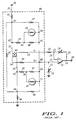
- FIG. 1 shows a prior art circuit board sensor assembly comprising a sensor integrated circuit 40 and other electrical components including an op amp 15.
- FIG. 2 shows a matched pair of sensor and amplifier circuits according to a preferred embodiment of the present invention, including sensor circuit 140 and amplifier circuit 160.
- FIG. 3 shows a matched pair of sensor and amplifier circuits according to an alternative embodiment of the present invention, including sensor circuit 240 and amplifier circuit 260.
- FIG. 1 shows a prior art circuit board sensor assembly comprising a sensor integrated circuit 40, including transducer 50, and other electrical components including an op amp 15 and trim resistors 12 and 14. Resistor 14 is used to adjust the gain of op amp 15, while resistor 12 is used to adjust the offset of op amp 15. As mentioned above, the sensor assembly shows in FIG. 1 has the disadvantage of requiring the customer or user to trim resistor 12 and 14. This can be a fairly complicated procedure because the assembly must be subjected to at least two different pressures at each of at least two different temperatures.
- circuit board sensor assembly requires the user to design and characterize a specific circuit.
- the user must obtain and assemble the various components of the circuit board assembly.
- FIG. 2 shows a matched pair of sensor and amplifier circuits according to a preferred embodiment of the present invention, including sensor circuit 140 and amplifier circuit 160.
- Sensor circuit 140 is implemented as an integrated circuit having external terminals 201-208.
- Sensor circuit 140 comprises a sensor transducer 150 having a positive output 134, a negative output 133, and excitation terminals 132 and 135. As is well known, an increase in pressure on transducer 150 creates a voltage differential across output terminals 133 and 134, the differential increasing proportional to the applied pressure.
- Sensor circuit 140 also comprises temperature-compensating resistors, such as resistors 152 and 154.
- Resistors 152 and 154 are conveniently but not essentially provided as thin-film resistors. Any trimmable monolithic form of resistors may be used.
- resistors 141-149, 151, 153, and 155-158 are provided on IC 140.
- Resistors 141-149, 151, 153, and 155-158 may also be thin-film resistors.
- Amplifier circuit 160 comprises a pair of op amps 180 and 190, each having an inverting input (181, 191), a non-inverting input (182, 192), and an output (185, 195).
- the negative output 133 of sensor 150 is coupled to the non-inverting input 182 of op amp 180 through terminal 206.
- the positive output 134 of sensor 150 is coupled to the non-inverting input 192 of op amp 190 through terminal 207.
- a resistor network comprises resistors 149, 151, 153, 155, and 156.
- Resistors 149, 151, and 156 form a resistive divider network which is used to set the temperature coefficient of the offset of op amp 180.
- Resistor 149 is coupled between positive power supply terminal 130′ and junction 172, and resistor 151 is coupled between junction 172 and ground.
- One side of resistor 153 is coupled via output terminal 202 to the output 195 of op amp 190, and the other side of resistor 153 is coupled to junction 174.
- One side of resistor 155 is coupled to junction 174, and the other side of resistor 155 is coupled to junction 175.
- Junction 174 is coupled through output terminal 203 to the inverting input 191 of op amp 190.
- resistor 156 One side of resistor 156 is coupled to junction 173 which is also coupled to junction 172, and the other side of resistor 156 is coupled to junction 175, which is coupled through output terminal 204 to the output of op amp 180.
- Junction 173 is coupled through output terminal 205 to the inverting input 181 of op amp 180.
- a positive supply voltage is applied to IC 140 at terminal 201.
- Terminal 208 is coupled to ground.
- the circuit output voltage is produced at output terminal 220.
- amplifier circuit 160 may be implemented either as a circuit board or integrated circuit.
- the matched sensor-amplifier arrangement of FIG. 2 can be provided as two die in a single package, as a two-chip assembly, or as two packages marketed together in a single envelope.
- trimmable passive components are located on sensor IC 140.
- the outputs at terminal 206 and 207 are nominally equal and remain so over the temperature range.
- the networks comprising resistors 152 and 154 draw more or less current, causing the positive sensor output 134 to track the negative sensor output 133.
- the thin-film resistors 141 and 146 are trimmed to compensate the sensor span for temperature.
- the span can be compensated for temperature, for example, over a range of between -40° Centigrade to 125° Centigrade, with slightly less accuracy outside of that range.
- resistor 143 or resistor 145 is trimmed to provide the absolute offset of sensor 150 at room temperature.
- resistor 149 or 151 is trimmed to match the voltage at junction 172 to junction 175 at room temperature.
- Resistor 156 is then trimmed until output 220 returns to the room temperature absolute offset.
- resistor 153 is trimmed until the correct output at 220 is produced.
- FIG. 3 shows a matched pair of sensor and amplifier circuits according to an alternative embodiment of the present invention, including sensor circuit 240 and amplifier circuit 260.
- FIG. 2 also applies to the circuit of FIG. 3, wherein the trim elements are located on the sensor IC 240. But the sensor IC 240 is implemented slightly differently from sensor IC 140, and the amplifier circuit 260 comprises only one op amp 290 in this implementation.
- Sensor IC circuit 240 comprises sensor transducer 250 having a positive output 234, a negative output 233, and excitation terminals 232 and 235. Circuit 240 also comprises monolithic temperature-compensating resistors 252 and 254 of, for example, thin-film resistive material.
- Sensor circuit 240 also comprises trimmable resistors 241-249, 251, and 253. Also included are temperature-compensating resistors 252 and 254 and adjustable resistive elements 255 and 257. Thin-film resistors which may be laser-trimmed are preferred, but other trimmable resistor materials and other trimming techniques well known in the art may also be used.
- Adjustable resistive element 255 is used to set the gain of op amp 290, and resistive element 257 is used to adjust the offset of op amp 290.
- the output 275 of op amp 290 is fed back to the inverting input 291 via terminal 302, resistive element 255, junction 272 and terminal 303.
- the non-inverting input 292 of op amp 290 is coupled to one junction 273 of resistive element 257 via terminal 304. Junction 273 is also coupled to the positive output 234 of sensor 250 through junction 268 and resistor 247.
- Sensor IC 240 has external terminals 301-305. A positive supply voltage is applied to IC 240 at terminal 301. Terminal 305 is coupled to ground. The circuit output voltage is produced at output terminal 320 of amplifier circuit 260.
- the thin-film resistors 241 and 249 are trimmed to compensate the sensor span for temperature.
- resistor 244 or resistor 248 is trimmed to provide the absolute offset of sensor 250 at room temperature.
- resistor 257 can be adjusted to provide the absolute offset instead of trimming resistors 244 and 248.
- the present invention provides a straight-forward, inexpensive solution to the requirement for short development cycles, relatively easy modification, short production cycles. Only seven mask layers are required, and no epitaxial or isolation diffusions are required, since there are no transistors on the sensor IC.
- Another advantage of the present invention is that by keeping the amplifier circuit off the sensor chip, the amplifier circuit can be mounted at a suitable distance from harsh environments to which the sensor IC may be exposed, e.g. the sensor may be mounted on an automotive engine manifold and the amplifier on the firewall.
- the present invention can be extended to any type of transducer, such as accelerometers, flow meters, force sensors, load cells, chemical sensors, humidity sensors, Hall effect sensors, industrial microphones, etc.
- transducer such as accelerometers, flow meters, force sensors, load cells, chemical sensors, humidity sensors, Hall effect sensors, industrial microphones, etc.
- temperature-compensating means could be used on the sensor IC in place of temperature-compensating resistors, such as diodes, active circuitry, or other temperature-compensating techniques.
- resistor-trimming methods such as pulse-trimming.
- the invention could be carried out by manufacturing the sensor IC, including trimming the resistors on the sensor IC, and putting the sensor IC's into inventory. At a later date, a sensor IC could be retrieved and matched with an amplifying circuit.
- the matching could be carried out by trimming the op amp(s) on the amplifying circuit, for example, by pulse-trimming the op amps.
- implant resistors could be used in addition to or in place of thin-film resistors on the sensor IC, and that such resistors could be trimmed using metal migration techniques.
Landscapes
- Physics & Mathematics (AREA)
- General Physics & Mathematics (AREA)
- Measuring Fluid Pressure (AREA)
- Indication And Recording Devices For Special Purposes And Tariff Metering Devices (AREA)
- Measurement Of Force In General (AREA)
- Measurement Of Length, Angles, Or The Like Using Electric Or Magnetic Means (AREA)
- Parts Printed On Printed Circuit Boards (AREA)
- Pressure Sensors (AREA)
- Amplifiers (AREA)
Description
- This invention relates generally to electronic sensor circuits, and, more particularly, to a sensor circuit assembly comprising a sensor integrated circuit and an amplifier circuit distinct from said sensor integrated circuit, wherein all system trim resistors are located on the sensor integrated circuit.
- The present invention has utility in electronic sensor circuits, especially in semiconductor pressure sensor circuits. Pressure responsive transducer circuits are utilized extensively in automobile engine control systems. For example, a manifold pressure sensor and amplifier circuit may provide an analog signal which varies with the engine manifold pressure. An analog-to-digital converter transforms the analog control signal into a digital control signal which is utilized by a microprocessor-controlled fuel injection system.
- US-A-4777826 describes a strain guage sensor with trimming and gain-setting resistors arranged in a thin film circuit for connection to an amplifier. The thin film circuit is formed of a single homogenous material and is inherently substantially unaffected by temperature.
- The operation of most semiconductor pressure transducers and op amps varies with temperature, requiring temperature-compensating techniques and circuitry. U.S. Patents 4,326,171 and 4,463,274 disclose temperature-compensating circuits for pressure transducers.
- Semiconductor transducer / amplifier circuits may be packaged in several ways. For example, they may be packaged on a printed circuit board. However, the customer is then responsible for performing the necessary trimming operations for temperature compensation and for adjusting the op amp gain. Customers typically may not be qualified or motivated to perform such work. Moreover, resistor temperature coefficients at the board level are not well matched, thus degrading system accuracy.
- Another known package is a two-chip system comprising a sensor chip and a second custom chip containing thin-film resistors for temperature compensation and for calibrating and amplifying the output. However, the disadvantages of the two-chip system are that the custom integrated circuit must be redesigned for each advance or alteration in circuit or process technology. Nor can a two-chip system provide necessary flexibility in circuit configuration.
- Yet another known package is a hybrid module, comprising a substrate on which is mounted a sensor chip, one or more amplifier chips, and suitable resistors and capacitors which are soldered to metal pads and wire-bonded to interconnecting metal traces. The resulting package may take the form of an encapsulated assembly with leads.
- One disadvantage of hybrid modules is that they tend to be very labor intensive because each component has to be individually placed, connected, calibrated, and temperature-compensated.
- It is also known to incorporate sensor circuits onto a single integrated circuit device. But even with a fully integrated circuit device it is necessary to adjust or "trim" on-chip passive elements for various purposes, such as setting the transducer offset voltage, the op amp input voltage offset, and resistive values.
- An advantage of a fully integrated device is that all trim is performed on a system-wide basis. That is, the op amp gain is set at the same time that the sensor element temperature calibration step is performed. All components on the chip, including the sensor and op amps, are matched with respect to values and temperature coefficients. At trim, all values and temperature coefficients are set.
- However, a disadvantage of such integrated circuit devices is that they have relatively long development cycles and are relatively expensive, especially in low-volume applications.
- There is therefore a significant need in the semiconductor transducer field to provide customers with a fully system-ready product, which requires no trimming or adjustment by the customer or user. There is also a strong demand by customers for relatively low cost sensor circuits. In addition, customers desire short development cycles for prototype sensor systems, so it would be desirable to provide a sensor assembly that is easy to modify to meet the needs of different customer applications.
- Therefore, there is a substantial need to provide a compact sensor assembly that is low in cost, high in quality, and which facilitates a short prototyping cycle and a short manufacturing cycle.
- In accordance with a first aspect of the invention, there is provided a matched sensor-amplifier assembly comprising an integrated circuit having a sensor, temperature compensating adjustable resistive means and pressure compensating adjustable resistive means, and a separate amplifier circuit having an amplifier, wherein the integrated circuit and the amplifier circuit are coupled together, characterized in that: the temperature compensating adjustable resistive means and the pressure compensating adjustable resistive means are contained in the integrated circuit, and the temperature compensating adjustive resistive means and the pressure compensating adjustive means are adjusted under various conditions so that the integrated circuit and the amplifier circuit form a matched pair, wherein the matched pair is formed during manufacture of the assembly.
- In a preferred embodiment, the temperature compensating adjustable resistive means are set to minimize temperature variation of an output of the matched sensor-amplifier assembly when together, so as to provide the matched pair.
- Furthermore, the temperature compensating adjustable resistive means are set to provide a predetermined output off-set for the matched sensor-amplifier assembly when together, so as to provide the matched pair.
- In the preferred embodiment, the matched sensor-amplifier assembly may be mounted in apparatus, wherein the integrated circuit is located in a position on the apparatus which is subject to temperature variation when the apparatus is in use and the amplifier circuit is located remote from the integrated circuit in a position on the apparatus which is relatively stable in temperature when in use.
- In a further aspect of the invention, there is provided a method of manufacturing a matched sensor-amplifier assembly having a predetermined temperature characteristic comprising the steps of: providing an integrated circuit comprising a sensor and temperature compensating adjustable resistive means; providing an amplifier circuit, separate from the integrated circuit, comprising an amplifier; coupling the sensor and the temperature compensating resistive means to the amplifier circuit such that the temperature compensating resistive means are arranged to adjust gain and/or offset of the amplifier, the method characterized by the steps of: placing the temperature compensating adjustable resistive means within the integrated circuit; subjecting the sensor to a first predetermined temperature and adjusting the temperature compensating adjustable resistive means; and subjecting the sensor to a second, different predetermined temperature and adjusting the temperature compensating adjustable resistive means, thereby forming a matched sensor-amplifier assembly with predetermined temperature characteristics, wherein the matched sensor-amplifier assembly is formed during manufacture.
- A preferred method of the further aspect includes the additional steps of: providing pressure compensating adjustable resistive means in the integrated circuit; coupling the pressure compensating adjustable resistive means to the amplifier circuit (160, 260) such that the pressure compensating adjustable resistive means (153, 255) are arranged to adjust the gain and/or offset of the amplifier; performing the steps of subjecting the sensor to the first predetermined temperature and adjusting the temperature compensating adjustable resistive means, and subjecting the sensor to the second, different predetermined temperature and adjusting the temperature compensating adjustable resistive means; subjecting the sensor to a change of pressure, and adjusting the pressure compensating adjustable resistive means, thereby forming a matched sensor-amplifier assembly with predetermined temperature and output characteristics, wherein the matched sensor-amplifier assembly is formed during manufacture.
- Furthermore, the preferred method may also include the step of providing a compensation element in the integrated circuit for determining datum pressure off-set and adjusting the compensation element to provide a predetermined datum pressure off-set for the matched sensor-amplifier assembly.
- In summary, the present invention fulfills the above-mentioned requirements by providing a sensor chip containing the desired trim resistors and a separate module containing only the amplifier(s). The amplifier module may take the form of a board or chip. All trim operations are performed at the factory on the combination integrated circuit / amplifier module.
- Exemplary embodiments of the invention will now be described with reference to the accompanying drawings.
- The invention is pointed out with particularity in the appended claims. However, other features of the intention will become more apparent and the invention will be best understood by referring to the following detailed description in conjunction with the accompanying drawings in which:
- FIG. 1 shows a prior art circuit board sensor assembly comprising a sensor integrated
circuit 40 and other electrical components including anop amp 15. - FIG. 2 shows a matched pair of sensor and amplifier circuits according to a preferred embodiment of the present invention, including
sensor circuit 140 andamplifier circuit 160. - FIG. 3 shows a matched pair of sensor and amplifier circuits according to an alternative embodiment of the present invention, including
sensor circuit 240 andamplifier circuit 260. - FIG. 1 shows a prior art circuit board sensor assembly comprising a sensor integrated
circuit 40, includingtransducer 50, and other electrical components including anop amp 15 andtrim resistors Resistor 14 is used to adjust the gain ofop amp 15, whileresistor 12 is used to adjust the offset ofop amp 15. As mentioned above, the sensor assembly shows in FIG. 1 has the disadvantage of requiring the customer or user to trimresistor - Because many users are not experienced circuit designers, they may encounter difficulties, since the prior art circuit board sensor assembly requires the user to design and characterize a specific circuit. In addition, the user must obtain and assemble the various components of the circuit board assembly.
- FIG. 2 shows a matched pair of sensor and amplifier circuits according to a preferred embodiment of the present invention, including
sensor circuit 140 andamplifier circuit 160.Sensor circuit 140 is implemented as an integrated circuit having external terminals 201-208. -
Sensor circuit 140 comprises asensor transducer 150 having apositive output 134, anegative output 133, andexcitation terminals transducer 150 creates a voltage differential acrossoutput terminals -
Sensor circuit 140 also comprises temperature-compensating resistors, such asresistors Resistors - All of the trimmable, passive elements in the sensor assembly, including resistors 141-149, 151, 153, and 155-158 are provided on
IC 140. Resistors 141-149, 151, 153, and 155-158 may also be thin-film resistors. -
Amplifier circuit 160 comprises a pair ofop amps - The
negative output 133 ofsensor 150 is coupled to thenon-inverting input 182 ofop amp 180 throughterminal 206. - The
positive output 134 ofsensor 150 is coupled to thenon-inverting input 192 ofop amp 190 throughterminal 207. - A resistor network comprises
resistors Resistors op amp 180. -
Resistor 149 is coupled between positivepower supply terminal 130′ andjunction 172, andresistor 151 is coupled betweenjunction 172 and ground. One side ofresistor 153 is coupled viaoutput terminal 202 to theoutput 195 ofop amp 190, and the other side ofresistor 153 is coupled tojunction 174. One side ofresistor 155 is coupled tojunction 174, and the other side ofresistor 155 is coupled tojunction 175. -
Junction 174 is coupled throughoutput terminal 203 to the invertinginput 191 ofop amp 190. - One side of
resistor 156 is coupled tojunction 173 which is also coupled tojunction 172, and the other side ofresistor 156 is coupled tojunction 175, which is coupled throughoutput terminal 204 to the output ofop amp 180. -
Junction 173 is coupled throughoutput terminal 205 to the invertinginput 181 ofop amp 180. - A positive supply voltage is applied to
IC 140 atterminal 201.Terminal 208 is coupled to ground. And the circuit output voltage is produced at output terminal 220. - It should be understood that
amplifier circuit 160 may be implemented either as a circuit board or integrated circuit. - The matched sensor-amplifier arrangement of FIG. 2 can be provided as two die in a single package, as a two-chip assembly, or as two packages marketed together in a single envelope.
- It should also be understood that the trimmable passive components are located on
sensor IC 140. - The operation of the circuit shown in FIG. 2 as pressure is applied to
sensor 150 will now be explained. - After the circuit-trimming operation has been completed (see below), with no pressure applied the outputs at
terminal networks comprising resistors positive sensor output 134 to track thenegative sensor output 133. - Again at room temperature, as pressure is applied,
positive sensor output 134 increases in voltage causing the output ofop amp 190 to increase. As the temperature is raised, the input resistance ofsensor 150 increases, the resistance of thin-film resistors sensor 150. - The various steps that occur in trimming the
sensor IC 140 after assembly and before it is shipped to the customer will now be described. - First, the thin-
film resistors -
Next resistor 143 orresistor 145 is trimmed to provide the absolute offset ofsensor 150 at room temperature. - Then
resistor junction 172 tojunction 175 at room temperature. - Next, the temperature is elevated to a higher temperature.
Resistor 156 is then trimmed until output 220 returns to the room temperature absolute offset. - Finally, pressure is increased to a higher pressure. Then
resistor 153 is trimmed until the correct output at 220 is produced. - FIG. 3 shows a matched pair of sensor and amplifier circuits according to an alternative embodiment of the present invention, including
sensor circuit 240 andamplifier circuit 260. - The basic concept seen in FIG. 2 also applies to the circuit of FIG. 3, wherein the trim elements are located on the
sensor IC 240. But thesensor IC 240 is implemented slightly differently fromsensor IC 140, and theamplifier circuit 260 comprises only oneop amp 290 in this implementation. -
Sensor IC circuit 240 comprisessensor transducer 250 having apositive output 234, anegative output 233, andexcitation terminals Circuit 240 also comprises monolithic temperature-compensatingresistors -
Sensor circuit 240 also comprises trimmable resistors 241-249, 251, and 253. Also included are temperature-compensatingresistors resistive elements - Adjustable
resistive element 255 is used to set the gain ofop amp 290, andresistive element 257 is used to adjust the offset ofop amp 290. - The
output 275 ofop amp 290 is fed back to the invertinginput 291 viaterminal 302,resistive element 255,junction 272 and terminal 303. Thenon-inverting input 292 ofop amp 290 is coupled to onejunction 273 ofresistive element 257 viaterminal 304.Junction 273 is also coupled to thepositive output 234 ofsensor 250 throughjunction 268 andresistor 247. -
Sensor IC 240 has external terminals 301-305. A positive supply voltage is applied toIC 240 atterminal 301.Terminal 305 is coupled to ground. The circuit output voltage is produced atoutput terminal 320 ofamplifier circuit 260. - The steps that occur in trimming the
sensor IC 240 after assembly and before it is shipped to the customer will now be described. - First, the thin-
film resistors -
Next resistor 244 orresistor 248 is trimmed to provide the absolute offset ofsensor 250 at room temperature. - Next, the temperature is elevated to a higher temperature, and
resistors output 320 returns to the room temperature absolute offset. Finally, pressure is increased to a higher pressure. Thenresistor 255 is trimmed until the correct output at 320 is produced. As an option,resistor 257 can be adjusted to provide the absolute offset instead of trimmingresistors - It will be apparent that the present invention provides a straight-forward, inexpensive solution to the requirement for short development cycles, relatively easy modification, short production cycles. Only seven mask layers are required, and no epitaxial or isolation diffusions are required, since there are no transistors on the sensor IC.
- Another advantage of the present invention is that by keeping the amplifier circuit off the sensor chip, the amplifier circuit can be mounted at a suitable distance from harsh environments to which the sensor IC may be exposed, e.g. the sensor may be mounted on an automotive engine manifold and the amplifier on the firewall.
- It will also be apparent to those skilled in the art that the disclosed invention may be modified in numerous ways and may assume many embodiments other than the preferred form specifically set out and described above.
- For example, the present invention can be extended to any type of transducer, such as accelerometers, flow meters, force sensors, load cells, chemical sensors, humidity sensors, Hall effect sensors, industrial microphones, etc.
- It will be apparent that other signal-conditioning circuits could be used to supplement or substitute for the amplifier circuit (i.e.
circuit 160 or 260). - Also, other temperature-compensating means could be used on the sensor IC in place of temperature-compensating resistors, such as diodes, active circuitry, or other temperature-compensating techniques.
- Moreover, it will be understood that other resistor-trimming methods may be used, such as pulse-trimming.
- In addition, the invention could be carried out by manufacturing the sensor IC, including trimming the resistors on the sensor IC, and putting the sensor IC's into inventory. At a later date, a sensor IC could be retrieved and matched with an amplifying circuit.
- Moreover, the matching could be carried out by trimming the op amp(s) on the amplifying circuit, for example, by pulse-trimming the op amps.
- It will be apparent that implant resistors could be used in addition to or in place of thin-film resistors on the sensor IC, and that such resistors could be trimmed using metal migration techniques.
Claims (8)
- A matched sensor-amplifier assembly comprising an integrated circuit (140, 240) having a sensor (150, 250), temperature compensating adjustable resistive means (141, 143, 145, 146, 149, 151, 155, 156, 241, 244, 248, 245, 249, 251, 252, 254, 257) and pressure compensating adjustable resistive means (153, 255), and a separate amplifier circuit (160, 260) having an amplifier (180, 190, 290), wherein the integrated circuit (140, 240) and the amplifier circuit (160, 260) are coupled together, characterized in that:
the temperature compensating adjustable resistive means (141, 143, 145, 146, 149, 151, 155, 156, 241, 244, 248, 245, 249, 251, 252, 254, 257) and the pressure compensating adjustable resistive means (153, 255) are contained in the integrated circuit (140, 240); and
the temperature compensating adjustable resistive means (141, 143, 145, 146, 149, 151, 155, 156, 241, 244, 248, 245, 249, 251, 252, 254, 257) and the pressure compensating adjustable resistive means (153, 255) are adjusted under various conditions so that the integrated circuit (140, 240) and the amplifier circuit (160, 260) form a matched pair, wherein the matched pair is formed during manufacture of the assembly. - A matched sensor-amplifier assembly according to claim 1, wherein the temperature compensating adjustable resistive means (141, 143, 145, 146, 149, 151, 155, 156, 241, 244, 248, 245, 249, 251, 252, 254, 257) are set to minimize temperature variation of an output (220, 320) of the matched sensor-amplifier assembly when together, so as to provide the matched pair.
- A matched sensor-amplifier assembly according to claim 1 or 2, wherein the temperature compensating adjustable resistive means (141, 143, 145, 146, 149, 151, 155, 156, 241, 244, 248, 245, 249, 251, 252, 254, 257) are set to provide a predetermined output off-set for the matched sensor-amplifier assembly when together, so as to provide the matched pair.
- A matched sensor-amplifier assembly according to claim 1, 2 or 3, wherein the integrated circuit (240) further comprises adjustable resistive means (257) for connection between an inverting (291) input and a non-inverting (292) input of the amplifier (290).
- A matched sensor-amplifier assembly according to any one of the preceding claims, mounted in an apparatus, wherein the integrated circuit (140, 240) is located in a position on the apparatus which is subject to temperature variation when the apparatus is in use and the amplifier circuit (160, 260) is located remote from the integrated circuit (140, 240) in a position on the apparatus which is relatively stable in temperature when in use.
- A method of manufacturing a matched sensor-amplifier assembly having a predetermined temperature characteristic, comprising the steps of:
providing an integrated circuit (140, 240) comprising a sensor (150, 250) and temperature compensating adjustable resistive means (141, 143, 145, 146, 149, 151, 155, 156, 241, 244, 248, 245, 249, 251, 252, 254, 257);
providing an amplifier circuit (160, 260), separate from the integrated circuit (140, 240), comprising an amplifier (180, 190, 290);
coupling the sensor (150, 250) and the temperature compensating resistive means (141, 143, 145, 146, 149, 151, 155, 156, 241, 244, 248, 245, 249, 251, 252, 254, 257) to the amplifier circuit (160, 260) such that the temperature compensating resistive means (141, 143, 145, 146, 149, 151, 155, 156, 241, 244, 248, 245, 249, 251, 252, 254, 257) are arranged to adjust gain and/or offset of the amplifier (180, 190, 290); the method characterized by the steps of:
locating the temperature compensating adjustable resistive means (141, 143, 145, 146, 149, 151, 155, 156, 241, 244, 248, 245, 249, 251, 252, 254, 257) within the integrated circuit (140, 240);
subjecting the sensor (150, 250) to a first predetermined temperature and adjusting the temperature compensating adjustable resistive means (141, 143, 145, 146, 149, 151, 155, 156, 241, 244, 248, 245, 249, 251, 252, 254, 257); and
subjecting the sensor to a second, different predetermined temperature and adjusting the temperature compensating adjustable resistive means (141, 143, 145, 146, 149, 151, 155, 156, 241, 244, 248, 245, 249, 251, 252, 254, 257), thereby forming a matched sensor-amplifier assembly with predetermined temperature characteristics, wherein the matched sensor-amplifier assembly is formed during manufacture. - A method according to claim 6, comprising the further steps of:
providing pressure compensating adjustable resistive means (153, 255) in the integrated circuit (140, 240);
coupling the pressure compensating adjustable resistive means (153, 155) to the amplifier circuit (160, 260) such that the pressure compensating adjustable resistive means (153, 255) are arranged to adjust the gain and/or offset of the amplifier (180, 190, 290);
performing the steps of subjecting the sensor to the first predetermined temperature and adjusting the temperature compensating adjustable resistive means (141, 143, 145, 146, 149, 151, 155, 156, 241, 244, 245, 248, 249, 251, 252, 254, 257), and subjecting the sensor (150, 250) to the second, different predetermined temperature and adjusting the temperature compensating adjustable resistive means (141, 143, 145, 146, 149, 151, 155, 156, 241, 244, 245, 248, 249, 251, 252, 254, 257);
subjecting the sensor (150, 250) to a change of pressure, and
adjusting the pressure compensating adjustable resistive means (153, 255), thereby forming a matched sensor-amplifier assembly with predetermined temperature and output characteristics, wherein the matched sensor-amplifier assembly is formed during manufacture. - A method according to claim 6 or 7, comprising the further steps of providing a compensation element (257) in the integrated circuit (240) for determining datum pressure off-set and adjusting the compensation element (257) to provide a predetermined datum pressure off-set for the matched sensor-amplifier assembly.
Applications Claiming Priority (2)
| Application Number | Priority Date | Filing Date | Title |
|---|---|---|---|
| US07/474,882 US5031461A (en) | 1990-02-05 | 1990-02-05 | Matched pair of sensor and amplifier circuits |
| US474882 | 1990-02-05 |
Publications (2)
| Publication Number | Publication Date |
|---|---|
| EP0441549A1 EP0441549A1 (en) | 1991-08-14 |
| EP0441549B1 true EP0441549B1 (en) | 1995-05-03 |
Family
ID=23885331
Family Applications (1)
| Application Number | Title | Priority Date | Filing Date |
|---|---|---|---|
| EP91300846A Expired - Lifetime EP0441549B1 (en) | 1990-02-05 | 1991-02-01 | Matched pair of sensor and amplifier circuits |
Country Status (4)
| Country | Link |
|---|---|
| US (1) | US5031461A (en) |
| EP (1) | EP0441549B1 (en) |
| JP (1) | JPH04213020A (en) |
| DE (1) | DE69109320T2 (en) |
Families Citing this family (5)
| Publication number | Priority date | Publication date | Assignee | Title |
|---|---|---|---|---|
| NO954729L (en) * | 1995-01-03 | 1996-07-04 | Motorola Inc | Follower circuit and compensation procedure |
| US5759870A (en) * | 1995-08-28 | 1998-06-02 | Bei Electronics, Inc. | Method of making a surface micro-machined silicon pressure sensor |
| US6581468B2 (en) | 2001-03-22 | 2003-06-24 | Kavlico Corporation | Independent-excitation cross-coupled differential-pressure transducer |
| AT413921B (en) | 2002-10-01 | 2006-07-15 | Akg Acoustics Gmbh | MICROPHONES WITH A SAME SENSITIVITY AND METHOD FOR THE PRODUCTION THEREOF |
| US20050267664A1 (en) * | 2004-05-14 | 2005-12-01 | Jiyuan Ouyang | Method for adjusting a control signal of an electronic sensor |
Family Cites Families (8)
| Publication number | Priority date | Publication date | Assignee | Title |
|---|---|---|---|---|
| US3368179A (en) * | 1966-03-30 | 1968-02-06 | Gen Electric | Temperature compensated semiconductor strain gage |
| US4355537A (en) * | 1980-11-06 | 1982-10-26 | Combustion Engineering, Inc. | Temperature compensation for transducer components |
| JPS59117271A (en) * | 1982-12-24 | 1984-07-06 | Hitachi Ltd | Semiconductor device having pressure sensing element and manufacture thereof |
| US4777826A (en) * | 1985-06-20 | 1988-10-18 | Rosemount Inc. | Twin film strain gauge system |
| IT1183962B (en) * | 1985-09-17 | 1987-10-22 | Marelli Autronica | INTERFACE CIRCUITS BETWEEN A SENSOR IN PARTICULAR A PRESSURE SENSOR OF THE THICK FILM TYPE AND AN INSTRUMENT ELECTRODYNAMIC INDICATOR AND INCORPORATING SENSOR SUCH CIRCUIT FOR PARTICULAR USE ON BOARD VEHICLES |
| JPH0797010B2 (en) * | 1986-03-26 | 1995-10-18 | 株式会社日立製作所 | Semiconductor strain gage bridge circuit |
| DE3736904A1 (en) * | 1987-10-30 | 1989-05-11 | Nord Micro Elektronik Feinmech | MEASURING DEVICE WITH SENSOR ELEMENTS |
| US4864463A (en) * | 1988-04-19 | 1989-09-05 | Allied-Signal Inc. | Capacitive pressure sensor |
-
1990
- 1990-02-05 US US07/474,882 patent/US5031461A/en not_active Expired - Fee Related
-
1991
- 1991-01-29 JP JP3028115A patent/JPH04213020A/en active Pending
- 1991-02-01 EP EP91300846A patent/EP0441549B1/en not_active Expired - Lifetime
- 1991-02-01 DE DE69109320T patent/DE69109320T2/en not_active Expired - Fee Related
Also Published As
| Publication number | Publication date |
|---|---|
| EP0441549A1 (en) | 1991-08-14 |
| JPH04213020A (en) | 1992-08-04 |
| DE69109320T2 (en) | 1995-12-07 |
| US5031461A (en) | 1991-07-16 |
| DE69109320D1 (en) | 1995-06-08 |
Similar Documents
| Publication | Publication Date | Title |
|---|---|---|
| CA2145698C (en) | Electronic circuit for a transducer | |
| US8186226B2 (en) | Pressure sensor with on-board compensation | |
| US5187985A (en) | Amplified pressure transducer | |
| US4333349A (en) | Binary balancing apparatus for semiconductor transducer structures | |
| EP0358352B1 (en) | Temperature compensation circuit | |
| US3956927A (en) | Strain gauge transducer apparatus | |
| JPH038482B2 (en) | ||
| EP1677089B1 (en) | Integrated pressure sensor and method of manufacture | |
| JPH08510549A (en) | Strain gauge sensor with integrated temperature signal output | |
| US4463274A (en) | Temperature compensation circuit for pressure sensor | |
| US5134885A (en) | Circuit arrangement for measuring a mechanical deformation, in particular under the influence of a pressure | |
| US4836027A (en) | Circuit for a sensor | |
| EP0441549B1 (en) | Matched pair of sensor and amplifier circuits | |
| EP0456811B1 (en) | Multi-variable sensor calibration | |
| US5854421A (en) | Semiconductor sensors and method for adjusting the output | |
| US6011422A (en) | Integrated differential voltage amplifier with programmable gain and input offset voltage | |
| JPH10281897A (en) | Semiconductor pressure detector | |
| Kopystynski et al. | An interchangeable silicon pressure sensor with on-chip compensation circuitry | |
| US6490926B2 (en) | Acceleration sensor module | |
| Weber et al. | A monolithically integrated sensor system using sensor-specific CMOS cells | |
| KR100238776B1 (en) | Temperature compensation method for pressure sensor and apparatus using the same | |
| JPH02218171A (en) | Semiconductor pressure sensor | |
| Otter et al. | A monolithic compensated silicon pressure transducer with temperature output for biomedical applications | |
| JPH09210831A (en) | Sensor module and its characteristic adjusting method | |
| JPH02271565A (en) | Semiconductor device |
Legal Events
| Date | Code | Title | Description |
|---|---|---|---|
| PUAI | Public reference made under article 153(3) epc to a published international application that has entered the european phase |
Free format text: ORIGINAL CODE: 0009012 |
|
| AK | Designated contracting states |
Kind code of ref document: A1 Designated state(s): DE FR GB IT |
|
| 17P | Request for examination filed |
Effective date: 19911007 |
|
| 17Q | First examination report despatched |
Effective date: 19930607 |
|
| GRAA | (expected) grant |
Free format text: ORIGINAL CODE: 0009210 |
|
| AK | Designated contracting states |
Kind code of ref document: B1 Designated state(s): DE FR GB IT |
|
| PG25 | Lapsed in a contracting state [announced via postgrant information from national office to epo] |
Ref country code: IT Free format text: LAPSE BECAUSE OF FAILURE TO SUBMIT A TRANSLATION OF THE DESCRIPTION OR TO PAY THE FEE WITHIN THE PRE;WARNING: LAPSES OF ITALIAN PATENTS WITH EFFECTIVE DATE BEFORE 2007 MAY HAVE OCCURRED AT ANY TIME BEFORE 2007. THE CORRECT EFFECTIVE DATE MAY BE DIFFERENT FROM THE ONE RECORDED.SCRIBED TIME-LIMIT Effective date: 19950503 Ref country code: FR Effective date: 19950503 |
|
| REF | Corresponds to: |
Ref document number: 69109320 Country of ref document: DE Date of ref document: 19950608 |
|
| EN | Fr: translation not filed | ||
| PGFP | Annual fee paid to national office [announced via postgrant information from national office to epo] |
Ref country code: DE Payment date: 19960130 Year of fee payment: 6 |
|
| PLBE | No opposition filed within time limit |
Free format text: ORIGINAL CODE: 0009261 |
|
| STAA | Information on the status of an ep patent application or granted ep patent |
Free format text: STATUS: NO OPPOSITION FILED WITHIN TIME LIMIT |
|
| 26N | No opposition filed | ||
| PGFP | Annual fee paid to national office [announced via postgrant information from national office to epo] |
Ref country code: GB Payment date: 19961219 Year of fee payment: 7 |
|
| PG25 | Lapsed in a contracting state [announced via postgrant information from national office to epo] |
Ref country code: DE Effective date: 19971101 |
|
| PG25 | Lapsed in a contracting state [announced via postgrant information from national office to epo] |
Ref country code: GB Free format text: LAPSE BECAUSE OF NON-PAYMENT OF DUE FEES Effective date: 19980201 |
|
| GBPC | Gb: european patent ceased through non-payment of renewal fee |
Effective date: 19980201 |