EP0441326A1 - A process for preparing a photo-recording medium - Google Patents
A process for preparing a photo-recording medium Download PDFInfo
- Publication number
- EP0441326A1 EP0441326A1 EP91101531A EP91101531A EP0441326A1 EP 0441326 A1 EP0441326 A1 EP 0441326A1 EP 91101531 A EP91101531 A EP 91101531A EP 91101531 A EP91101531 A EP 91101531A EP 0441326 A1 EP0441326 A1 EP 0441326A1
- Authority
- EP
- European Patent Office
- Prior art keywords
- group
- monomolecular film
- chemical adsorbent
- chemical
- diacetylene
- Prior art date
- Legal status (The legal status is an assumption and is not a legal conclusion. Google has not performed a legal analysis and makes no representation as to the accuracy of the status listed.)
- Granted
Links
Images


Classifications
-
- G—PHYSICS
- G11—INFORMATION STORAGE
- G11B—INFORMATION STORAGE BASED ON RELATIVE MOVEMENT BETWEEN RECORD CARRIER AND TRANSDUCER
- G11B7/00—Recording or reproducing by optical means, e.g. recording using a thermal beam of optical radiation by modifying optical properties or the physical structure, reproducing using an optical beam at lower power by sensing optical properties; Record carriers therefor
- G11B7/24—Record carriers characterised by shape, structure or physical properties, or by the selection of the material
- G11B7/26—Apparatus or processes specially adapted for the manufacture of record carriers
-
- B—PERFORMING OPERATIONS; TRANSPORTING
- B82—NANOTECHNOLOGY
- B82Y—SPECIFIC USES OR APPLICATIONS OF NANOSTRUCTURES; MEASUREMENT OR ANALYSIS OF NANOSTRUCTURES; MANUFACTURE OR TREATMENT OF NANOSTRUCTURES
- B82Y10/00—Nanotechnology for information processing, storage or transmission, e.g. quantum computing or single electron logic
-
- B—PERFORMING OPERATIONS; TRANSPORTING
- B82—NANOTECHNOLOGY
- B82Y—SPECIFIC USES OR APPLICATIONS OF NANOSTRUCTURES; MEASUREMENT OR ANALYSIS OF NANOSTRUCTURES; MANUFACTURE OR TREATMENT OF NANOSTRUCTURES
- B82Y30/00—Nanotechnology for materials or surface science, e.g. nanocomposites
-
- B—PERFORMING OPERATIONS; TRANSPORTING
- B82—NANOTECHNOLOGY
- B82Y—SPECIFIC USES OR APPLICATIONS OF NANOSTRUCTURES; MEASUREMENT OR ANALYSIS OF NANOSTRUCTURES; MANUFACTURE OR TREATMENT OF NANOSTRUCTURES
- B82Y40/00—Manufacture or treatment of nanostructures
Definitions
- the present invention relates to a process for preparing an optical recording medium.
- this invention relates to a process for preparing an optical recording medium with photochromic properties, which comprises a monomolecular film or a lamination of organic monomolecular films having polydiacetylenic bonds.
- Diacetylene derivative polymers have conductivity and nonlinear optical effects because of the presence of a ⁇ -electron conjugated system derived from polydiacetylenic bonds.
- these polymers are useful as optical- and electronic functional-materials such as optical recording media.
- optical recording media For example, as in the form of thin film such as monomolecular film.
- a thin polymer film that contains polydiacetylenic bonds is prepared by irradiating radioactive rays to a thin crystalline film of a diacetylene derivative compound.
- a single crystalline polydiacetylene thin film of large size cannot be obtained.
- the film is also prepared by irradiating radioactive rays to a monomolecular film formed by the Langmuir-Blodgett (LB) technique on a base plate, resulting in polymerization of the diacetylene groups.
- LB Langmuir-Blodgett
- the film prepared by this process has poor adhesiveness to the base plate.
- the film is susceptible to peeling from the base plate.
- the process will be expensive from a practical point of view because it is less efficient.
- the resulting optical recording medium has low density, and some pin-holes.
- the process for preparing an optical recording medium of this invention comprises: forming a monomolecular film on the surface of a base plate by adsorbing a chemical adsorbent having a diacetylene group, and a -SiCl group at one molecular end, and irradiating said monomolecular film with ultraviolet rays to polymerize said chemical addsorbent at the diacetylene group, thereby forming polydiacetylenic bonds.
- said chemical adsorbent is represented by the following formula I: wherein R1 and R2 are each independently H, an alkyl or alkoxy group having 1 to 4 carbon atoms, or halogen; l1, m1 and n1 are each independently 0 or larger integers; the sum of l1, m1 and n1 is from 5 to 25; and a1 is 0 or 1.
- said chemical adsorbent is any of the compounds represented by the following formulae: CH3-(CH2)2-C ⁇ C-C ⁇ C-(CH2)6-O-(CH2)3-SiCl3, CH3-CH2-C ⁇ C-C ⁇ C-(CH2)6-O-(CH2)3-SiCl3, CH3-C ⁇ C-C ⁇ C-(CH2)17-SiCl3, and H-C ⁇ C-C ⁇ C-(CH2)17-SiCl3
- At least one of said first and second chemical adsorbent has a substituent group on the carbon atom adjacent to said diacetylene group, and said substituent group can be conjugated with said polydiacetylenic bond, and said first and second chemical adsorbents are selected so that said first and second monomolecular films have different optical-absorption characteristics.
- At least one of said first and second chemical adsorbent is represented by the following formula II: wherein R3 and R4 are each independently H, an alkyl or alkoxyl group having 1 to 4 carbon atoms, or halogen; l2, m2 and n2 are 0 or larger integers; the sum of l2, m2 and n2 is from 5 to 25; and a2 is 0 or 1.
- another feature of this invention is a process for preparing an optical recording medium comprising: forming a first monomolecular film on the surface of a base plate by adsorbing a first chemical adsorbent having a diacetylene group, a -SiCl group at one molecular end, and a -SiH group at the other molecular end, irradiating said first monomolecular film with ultraviolet rays to polymerize said chemical adsorbent at the diacetylene group, thereby forming polydiacetylenic bonds, converting said a -SiH group into -SiOH group, forming a second monomolecular film on the surface of said polymerized first monomolecular film by adsorbing a second chemical adsorbent having a diacetylene group, and a -SiCl group at one molecular end, and irradiating said second monomolecular film with ultraviolet rays to polymer
- At least one of said first and second chemical adsorbent has a substituent group on the carbon atom adjacent to said diacetylene group, and said substituent group can be conjugated with said polydiacetylene group, and said first and second chemical adsorbents are selected so that said first and second monomolecular films have different optical-absorption characteristics.
- said first chemical adsorbent, or first and second chemical adsorbents are represented by the following formula III: wherein R5 and R6 are each independently an alkyl group having 1 to 4 carbon atoms; R7 and R8 are each independently H, an alkyl or alkoxy group having 1 to 4 carbon atoms, or halogen; l3, m3 and n3 are 0 or larger integers; the sum of l3, m3 and n3 is from 5 to 25; and a3 is 0 or 1.
- said first and second chemical adsorbents are the compound represented by the following formula:
- a chemical adsorbent used in the process for preparing a monomolecular film provided for optical recording media of this invention having a diacetylene group (-C ⁇ C-C ⁇ C-) and -SiCl group at one molecular end.
- the chemical adsorbent is for example, represented by the following formula I: wherein R1 and R2 are each independently H, an alkyl or alkoxy group having 1 to 4 carbon atoms, or halogen; l1, m1 and n1 are each independently 0 or larger integers; the sum of l1, m1 and n1 is from 5 to 25; and a1 is 0 or 1.
- Examples of the chemical adsorbent represented by the above-described formula I are illustrated below: CH3-(CH2)2-C ⁇ C-C ⁇ C-(CH2)6-O-(CH2)3-SiCl3 , CH3-CH2-C ⁇ C-C ⁇ C-(CH2)6-O-(CH2)3-SiCl3 , CH3-C ⁇ C-C ⁇ C-(CH2)17-SiCl3, and H-C ⁇ C-C ⁇ C-(CH2)17-SiCl3
- a chemical adsorbent represented by the following formula II or III can preferably be used: wherein R3 and R4 are each independently H, an alkyl or alkoxyl group having 1 to 4 carbon atoms, or halogen; l2, m2 and n2 are each independently 0 or larger integers; the sum of l2, m2 and n2 is from 5 to 25; and a2 is 0 or 1.
- R5 and R6 are each independently an alkyl group having 1 to 4 carbon atoms
- R7 and R8 are each independently H, an alkyl or alkoxy group having 1 to 4 carbon atoms, or halogen
- l3, m3 and n3 are each independently 0 or larger integers
- the sum of l3, m3 and n3 is from 5 to 25
- a3 is 0 or 1.
- a base plate having a functional group such as hydroxyl group, amino group, carboxyl group, and the like on its surface i.e., a base plate having a hydrophilic surface
- a silicon base plate having an oxidation film formed on its surface is preferably used.
- the oxidation film is formed by the treatment of the base plate with a thermal oxidation, or formed by natural oxidation.
- the base plate is immersed in a solution of a chemical adsorbent in a non-aqueous organic solvent.
- the organic solvent which can be used includes n-hexane, carbon tetrachloride, and the like, and mixtures thereof.
- concentration of the chemical adsorbent may be varied depending on the kinds of the base plate and its surface area, and is usually from 2.0 X 10 ⁇ 3 to 5.0 X 10 ⁇ 3 mol/L.
- the monomolecular film 3 formed on the base plate 1 is irradiated with ultraviolet rays to polymerize the adsorbent at the diacetylene group 2, thereby forming a polydiacetylenic bond 12 as shown in Figure 1b.
- the polydiacetylenic bond can also be formed by irradiating with X-rays, electron beams, or gamma rays instead of ultraviolet rays, all of which have higher energy than ultraviolet rays.
- a chemical adsorbent represented by the formula II or III is preferably used.
- first monomolecular film 3 is formed on the base plate 1 as described in Figure 1a by adsorbing the first chemical adsorbent of formula II.
- the first monomolecular film 3 is irradiated with ultraviolet rays to polymerize the chemical adsorbent at the diacetylene group 2 , thereby forming a polydiacetylenic bonds 12 ( Figure 1b).
- the base plate having the first monomolecular film is immersed into a solution of a second chemical adsorbent having a diacetylene group, and -SiCl group at one molecular end by the same procedure as described above with respect to the first chemical adsorbent.
- the second monomolecular film is formed on the surface of the first monomolecular film.
- the second monomolecular film is also irradiated with ultraviolet rays to polymerize the chemical adsorbent at the diacetylene group, thereby forming a polydiacetylene group 22 ( Figure 1d).
- the first monomolecular film 13 after irradiation is treated with an alkaline to convert the -SiH group at the molecular end into a -SiOH group. Then, the base plate having the first monomolecular film is immersed into a solution of the second chemical adsorbent, and the second monomolecular film thus obtained is also irradiated with ultraviolet rays, thereby forming polydiacetylenic bonds.
- a chemical adsorbent represented by the formula II or III is used as the second chemical adsorbent in each process for preparing the lamination of monomolecular films described above, and then repeating the above-mentioned procedure consecutively, a lamination that can be used for optical recording media having three, four or more monomolecular film layers can be obtained.
- the lamination of monomolecular films can also be prepared by forming a second monomolecular film on the surface of a first monomolecular film which is not irradiated with ultraviolet rays, and then irradiating this lamination of monomolecular films with ultraviolet rays to proceed polymerization in the first and second monomolecular films, thereby forming polydiacetylenic bonds in both films.
- a chemical adsorbent having oxygen in its principal chain i.e., a compound represented by the formula I, II or III wherein a1, a2 or a3 is 1, is used
- the chemical adsorbent molecules formed on the base plate will rotate more easily. Therefore, the diacetylene group in the chemical adsorbent molecule readily reacts with the diacetylen group that is present in the neiboring molecule to form polydiacetylenic bonds.
- a monomolecular film or a lamination of monomolecular films with high polymerization degree, and with longer conjugated systems can be obtained.
- the monomolecular film or a lamination of monomolecular films having longer conjugated systems provides optical recording media of higher quality.
- the resulting first and second monomolecular films may have different optical-absorption characteristics.
- a lamination having two monomolecular films, each with different optical-absorption characteristics can be used as a multiple optical recording medium.
- a chemical adsorbent having a substituent group on the carbon atom adjacent to the diacetylene group can be preferably be used. It is desirable that the substituent group be conjugated with the resulting polydiacetylenic bond.
- the substituents used include benzene ring, benzene condensed rings, amino group, amide group, carboxyl group, and the like. These substituents provide a monomolecular film having longer conjugated systems, and a higher degree of polymerization.
- an optical recording medium with higher recording sensitivity can be obtained.
- the coloring matter for sensitization metallocyanine-type coloring matters, and phthalocyanine-type coloring matters can preferably be used.
- an additional optical recording medium can be prepared by using a chemical adsorbent having a group with photochromic properties, for example, spiropyran group.
- a monomolecular film with 10 to 50 ⁇ thickness is formed on a base plate, and optionally, another monomolecular film is layered thereon.
- the monomolecular film or the lamination is radiated with ion laser beams, it will turn from blue to red.
- the film or the lamination is useful for optical recording media.
- a semiconductive silicon base plate, the surface of which, has been oxidized by a thermal oxidation to form SiO2 was provided.
- the chemical adsorbent was dissolved into a mixed solvent containing 80 wt% of n-hexane, 12 wt% of carbon tetrachloride, and 8 wt% of chloroform in a concentration of 1 X 10 ⁇ 3 mol/L.
- the aforementioned silicon base plate was immersed into this solution.
- the first monomolecular film 3 was irradiated with an ultraviolet ray L having a wavelength of 200-400 nm to polymerize the chemical adsorbent, thereby forming a polymerized blue monomolecular film 13 having polydiacetylenic bonds 12 (See, Figure 1b).
- the monomolecular film was irradiated with ultraviolet rays at two different radiation doses, and then its Raman scattering spectrum was observed (Figure 2, Spectrums B and C).
- the same kind of chemical adsorbents were used to form the first and second monomolecular films, but a different kind of chemical adsorbent can also be used to form the second monomolecular film.
- the second monomolecular film was irradiated with ultraviolet rays by the same procedure as described above, resulting in a lamination of monomolecular film with a blue color.
- an additional monomolecular film can be layered on the second monomolecular film by repeating the same procedures.
- the blue-colored lamination of monomolecular polymer films containing diacetylenic bonds as prepared above turned red when irradiated with an Ar ion laser beam, indicating that it can be used for optical recording process.
- the absorption spectrum of the irradiated lamination was identical to the absorption spectrum when the lamination was heated, and therefore it was confirmed that this reaction of color changes is due to the temperature increase of the monomolecular film caused by the radiation.
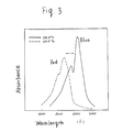
- Figure 3 shows a chart of the absorption spectrum of the lamination observed at the temperatures of 23.5°C and 60°C.
- the red optical recording medium turned blue again by cooling (i.e., the annealing effect). Therefore, in order to perform a permanent photorecording, the optical recording medium is irradiated with for example, an Ar ion laser beam so that its temperature can increase to more than 70°C, and especially 80°C. On the other hand, as long as the optical recording medium is irradiated under the condition that the temperature of the irradiated portion is 70°C or less, it can be used as a ereasable type medium.
- a lamination of monomolecular films that can be used for an optical recording medium was prepared by the same procedure as in Example 1 except that a chemical adsorbent represented by the following formula was used, and that the base plate having the polymerized first monomolecular film is immersed into a NaOH solution of p H12 to convert the -SiH group at the molecular end into a -SiOH group:
Abstract
Description
- The present invention relates to a process for preparing an optical recording medium. In particular, this invention relates to a process for preparing an optical recording medium with photochromic properties, which comprises a monomolecular film or a lamination of organic monomolecular films having polydiacetylenic bonds.
- Diacetylene derivative polymers have conductivity and nonlinear optical effects because of the presence of a π-electron conjugated system derived from polydiacetylenic bonds. Thus, these polymers are useful as optical- and electronic functional-materials such as optical recording media. For example, as in the form of thin film such as monomolecular film.
- A thin polymer film that contains polydiacetylenic bonds is prepared by irradiating radioactive rays to a thin crystalline film of a diacetylene derivative compound. However, according to this process, a single crystalline polydiacetylene thin film of large size cannot be obtained. The film is also prepared by irradiating radioactive rays to a monomolecular film formed by the Langmuir-Blodgett (LB) technique on a base plate, resulting in polymerization of the diacetylene groups.
- According to this process, a polydiacetylene derivative thin film of relatively large size can be obtained. However, the film prepared by this process has poor adhesiveness to the base plate. Thus, when the optical recording medium that contains this monomolecular film is worked, the film is susceptible to peeling from the base plate. Moreover, the process will be expensive from a practical point of view because it is less efficient. Also, the resulting optical recording medium has low density, and some pin-holes.
- The process for preparing an optical recording medium of this invention, which overcomes the above-discussed and numerous other disadvantages and deficiencies of the prior art, comprises:
forming a monomolecular film on the surface of a base plate by adsorbing a chemical adsorbent having a diacetylene group, and a -SiCl group at one molecular end, and
irradiating said monomolecular film with ultraviolet rays to polymerize said chemical addsorbent at the diacetylene group, thereby forming polydiacetylenic bonds. - In a preferred embodiment, said chemical adsorbent is represented by the following formula I:

wherein R1 and R2 are each independently H, an alkyl or alkoxy group having 1 to 4 carbon atoms, or halogen; ℓ1, m1 and n1 are each independently 0 or larger integers; the sum of ℓ1, m1 and n1 is from 5 to 25; and a1 is 0 or 1. - In a preferred embodiment, said chemical adsorbent is any of the compounds represented by the following formulae:
CH₃-(CH₂)₂-C≡C-C≡C-(CH₂)₆-O-(CH₂)₃-SiCl₃,
CH₃-CH₂-C≡C-C≡C-(CH₂)₆-O-(CH₂)₃-SiCl₃,
CH₃-C≡C-C≡C-(CH₂)₁₇-SiCl₃,
and
H-C≡C-C≡C-(CH₂)₁₇-SiCl₃
- Another feature of this invention is a process for preparing an optical recording medium comprising:
forming a first monomolecular film on the surface of a base plate by adsorbing a first chemical adsorbent having a diacetylene group, a -SiCl group at one molecular end, and a -CH=CH₂ group at the other molecular end,
irradiating said first monomolecular film with ultraviolet rays to polymerize said chemical adsorbent at the diacetylene group, thereby forming polydiacetylenic bonds,
converting said -CH=CH₂ group into a -CH₂-CH₂OH group,
forming a second monomolecular film on the surface of said polymerized first monomolecular film by adsorbing a second chemical adsorbent having a diacetylene group, and a -SiCl group at one molecular end, and
irradiating said second monomolecular film with ultraviolet rays to polymerize said chemical adsorbent at the diacetylene group, thereby forming polydiacetylenic bonds. - In a preferred embodiment, at least one of said first and second chemical adsorbent has a substituent group on the carbon atom adjacent to said diacetylene group, and said substituent group can be conjugated with said polydiacetylenic bond, and said first and second chemical adsorbents are selected so that said first and second monomolecular films have different optical-absorption characteristics.
- In a preferred embodiment, at least one of said first and second chemical adsorbent is represented by the following formula II:

wherein R3 and R4 are each independently H, an alkyl or alkoxyl group having 1 to 4 carbon atoms, or halogen; ℓ2, m2 and n2 are 0 or larger integers; the sum of ℓ2, m2 and n2 is from 5 to 25; and a2 is 0 or 1. - In a preferred embodiment, at least one of said first and second chemical adsorbent is the compound represented by the following formula:
CH₂=CH-(CH₂)₆-C≡C-C≡C(CH₂)₄-O-(CH₂)₃-SiCl₃
- Moreover, another feature of this invention is a process for preparing an optical recording medium comprising:
forming a first monomolecular film on the surface of a base plate by adsorbing a first chemical adsorbent having a diacetylene group, a -SiCl group at one molecular end, and a -SiH group at the other molecular end,
irradiating said first monomolecular film with ultraviolet rays to polymerize said chemical adsorbent at the diacetylene group, thereby forming polydiacetylenic bonds,
converting said a -SiH group into -SiOH group,
forming a second monomolecular film on the surface of said polymerized first monomolecular film by adsorbing a second chemical adsorbent having a diacetylene group, and a -SiCl group at one molecular end, and
irradiating said second monomolecular film with ultraviolet rays to polymerize said chemical adsorbent at the diacetylene group, thereby forming polydiacetylenic bonds. - In a preferred embodiment, at least one of said first and second chemical adsorbent has a substituent group on the carbon atom adjacent to said diacetylene group, and said substituent group can be conjugated with said polydiacetylene group, and said first and second chemical adsorbents are selected so that said first and second monomolecular films have different optical-absorption characteristics.
- In a preferred embodiment, said first chemical adsorbent, or first and second chemical adsorbents are represented by the following formula III:

wherein R5 and R6 are each independently an alkyl group having 1 to 4 carbon atoms; R7 and R8 are each independently H, an alkyl or alkoxy group having 1 to 4 carbon atoms, or halogen; ℓ3, m3 and n3 are 0 or larger integers; the sum of ℓ3, m3 and n3 is from 5 to 25; and a3 is 0 or 1. - In a preferred embodiment, said first and second chemical adsorbents are the compound represented by the following formula:

- Thus, the invention described herein makes possible the objectives of:
- (1) providing a process for preparing an optical recording medium which comprises the preparation of a monomolecular film or a lamination of monomolecular films having polydiacetylenic bonds formed on a base plate, the said optical recording medium having excellent adhesiveness between the base plate and monomolecular film, and optionally each monomolecular film;
- (2) providing a process for preparing an optical recording medium which comprises the preparation of a monomolecular film or a lamination of monomolecular films having polydiacetylenic bonds, the said film or lamination having higher density and less pinholes than those prepared by the conventional LB technique;
- (3) providing less expensive and easier process for preparing an optical recording medium that contains the above-described monomolecular film or the lamination thereof with a larger area and having better properties than the conventional LB technique;
- (4) providing a process for preparing an optical recording medium which comprises the preparation of a lamination of monomolecular films having polydiacetylenic bonds, the said lamination being applicable for use in multiple optical recording media; and
- (5) providing a process for preparing an optical recording medium which comprises the preparation of a monomolecular film or lamination of monomolecular films, especially having polydiacetylenic bonds, the said film or lamination having a high polymerization degree when a chemical adsorbent having oxygen in its principal chain is used.
- This invention may be better understood and its numerous objects and advantages will become apparent to those skilled in the art by reference to the accompanying drawings as follows:
- Figure 1a-1d shows a process for preparing a lamination of monomolecular films used for optical recording media of this invention.
- Figure 2 shows a chart of Fourier transfer IR (FTIR) analyzed Raman spectrum of the monomolecular film irradiated with ultraviolet rays, and formed in step b as shown in Figure 1.
- Figure 3 shows a chart of the visible absorption spectrum of the monomolecular film prepared in Example 1 at the temperatures of 23.5°C and 60°C.
- A chemical adsorbent used in the process for preparing a monomolecular film provided for optical recording media of this invention, having a diacetylene group (-C≡C-C≡C-) and -SiCl group at one molecular end. The chemical adsorbent, is for example, represented by the following formula I:

wherein R1 and R2 are each independently H, an alkyl or alkoxy group having 1 to 4 carbon atoms, or halogen; ℓ1, m1 and n1 are each independently 0 or larger integers; the sum of ℓ1, m1 and n1 is from 5 to 25; and a1 is 0 or 1. - Examples of the chemical adsorbent represented by the above-described formula I are illustrated below:
CH₃-(CH₂)₂-C≡C-C≡C-(CH₂)₆-O-(CH₂)₃-SiCl₃,
CH₃-CH₂-C≡C-C≡C-(CH₂)₆-O-(CH₂)₃-SiCl₃,
CH₃-C≡C-C≡C-(CH₂)₁₇-SiCl₃,
and
H-C≡C-C≡C-(CH₂)₁₇-SiCl₃
- When a lamination of monomolecular films is formed, a chemical adsorbent represented by the following formula II or III can preferably be used:

wherein R3 and R4 are each independently H, an alkyl or alkoxyl group having 1 to 4 carbon atoms, or halogen; ℓ2, m2 and n2 are each independently 0 or larger integers; the sum of ℓ2, m2 and n2 is from 5 to 25; and a2 is 0 or 1. or
wherein R5 and R6 are each independently an alkyl group having 1 to 4 carbon atoms; R7 and R8 are each independently H, an alkyl or alkoxy group having 1 to 4 carbon atoms, or halogen; ℓ3, m3 and n3 are each independently 0 or larger integers; the sum of ℓ3, m3 and n3 is from 5 to 25; and a3 is 0 or 1. - Examples of the chemical adsorbents represented by the above-described formulas II and III are illustrated below:
CH₂=CH-(CH₂)₆-C≡C-C≡C-(CH₂)₄-O-(CH₂)₃-SiCl₃,
and

- In the process for preparing a monomolecular film for use in an optical recording medium of this invention, a base plate having a functional group such as hydroxyl group, amino group, carboxyl group, and the like on its surface (i.e., a base plate having a hydrophilic surface) is first provided. For example, a silicon base plate having an oxidation film formed on its surface is preferably used. The oxidation film is formed by the treatment of the base plate with a thermal oxidation, or formed by natural oxidation. Next, the base plate is immersed in a solution of a chemical adsorbent in a non-aqueous organic solvent. The organic solvent which can be used includes n-hexane, carbon tetrachloride, and the like, and mixtures thereof. The concentration of the chemical adsorbent may be varied depending on the kinds of the base plate and its surface area, and is usually from 2.0 X 10⁻³ to 5.0 X 10⁻³ mol/L. By this immersion procedure, the -Si-Cl group that is present in the chemical adsorbent reacts with a -OH group that is present on the base plate, so that the chemical adsorbent can be bound chemically to the surface of the base plate. When the chemical adsorbent having -SiCl₃ is used, the monomolecular film shown in Figure 1a is formed by the immersion procedure described above.
- Next, the monomolecular film 3 formed on the
base plate 1 is irradiated with ultraviolet rays to polymerize the adsorbent at thediacetylene group 2, thereby forming apolydiacetylenic bond 12 as shown in Figure 1b. The polydiacetylenic bond can also be formed by irradiating with X-rays, electron beams, or gamma rays instead of ultraviolet rays, all of which have higher energy than ultraviolet rays. - For preparing a lamination of monomolecular films, a chemical adsorbent represented by the formula II or III is preferably used. For example, first monomolecular film 3 is formed on the
base plate 1 as described in Figure 1a by adsorbing the first chemical adsorbent of formula II. The first monomolecular film 3 is irradiated with ultraviolet rays to polymerize the chemical adsorbent at thediacetylene group 2, thereby forming a polydiacetylenic bonds 12 (Figure 1b). Then, the polymerized firstmonomolecular film 13 is contacted with diborane THF solution followed by H₂O₂ solution that contains alkaline to convert the -CH=CH₂ group into a -CH₂-CH₂-OH group (Figure 1c). The same conversion reaction is conducted by irradiating the first monomolecular film with either X-rays, electron beams, gamma rays, etc., under oxygen atmosphere. Also, in the case of irradiating the first monomolecular film with X-rays, electron beams, gamma rays, etc., under nitrogen atmosphere, the -CH=CH₂ group is converted into a -NH₂ group. Then, the base plate having the first monomolecular film is immersed into a solution of a second chemical adsorbent having a diacetylene group, and -SiCl group at one molecular end by the same procedure as described above with respect to the first chemical adsorbent. By this immersion procedure, the second monomolecular film is formed on the surface of the first monomolecular film. The second monomolecular film is also irradiated with ultraviolet rays to polymerize the chemical adsorbent at the diacetylene group, thereby forming a polydiacetylene group 22 (Figure 1d). - When a chemical adsorbent of formula III is used, the first
monomolecular film 13 after irradiation is treated with an alkaline to convert the -SiH group at the molecular end into a -SiOH group. Then, the base plate having the first monomolecular film is immersed into a solution of the second chemical adsorbent, and the second monomolecular film thus obtained is also irradiated with ultraviolet rays, thereby forming polydiacetylenic bonds. - If a chemical adsorbent represented by the formula II or III is used as the second chemical adsorbent in each process for preparing the lamination of monomolecular films described above, and then repeating the above-mentioned procedure consecutively, a lamination that can be used for optical recording media having three, four or more monomolecular film layers can be obtained. The lamination of monomolecular films can also be prepared by forming a second monomolecular film on the surface of a first monomolecular film which is not irradiated with ultraviolet rays, and then irradiating this lamination of monomolecular films with ultraviolet rays to proceed polymerization in the first and second monomolecular films, thereby forming polydiacetylenic bonds in both films.
- When a chemical adsorbent having oxygen in its principal chain, i.e., a compound represented by the formula I, II or III wherein a1, a2 or a3 is 1, is used, the chemical adsorbent molecules formed on the base plate will rotate more easily. Therefore, the diacetylene group in the chemical adsorbent molecule readily reacts with the diacetylen group that is present in the neiboring molecule to form polydiacetylenic bonds. Thus a monomolecular film or a lamination of monomolecular films with high polymerization degree, and with longer conjugated systems, can be obtained. The monomolecular film or a lamination of monomolecular films having longer conjugated systems, provides optical recording media of higher quality.
- When the first chemical adsorbent is different from the second one, the resulting first and second monomolecular films may have different optical-absorption characteristics. A lamination having two monomolecular films, each with different optical-absorption characteristics can be used as a multiple optical recording medium.
- For preparing such a two-layered lamination, a chemical adsorbent having a substituent group on the carbon atom adjacent to the diacetylene group can be preferably be used. It is desirable that the substituent group be conjugated with the resulting polydiacetylenic bond. The substituents used, for example, include benzene ring, benzene condensed rings, amino group, amide group, carboxyl group, and the like. These substituents provide a monomolecular film having longer conjugated systems, and a higher degree of polymerization.
- When a coloring matter for sensitization can be mixed with a chemical adsorbent in the process of this invention, an optical recording medium with higher recording sensitivity can be obtained. As the coloring matter for sensitization, metallocyanine-type coloring matters, and phthalocyanine-type coloring matters can preferably be used. Also, an additional optical recording medium can be prepared by using a chemical adsorbent having a group with photochromic properties, for example, spiropyran group.
- According to the process of this invention described above, a monomolecular film with 10 to 50 Å thickness is formed on a base plate, and optionally, another monomolecular film is layered thereon. When, for example, the monomolecular film or the lamination is radiated with ion laser beams, it will turn from blue to red. Thus, the film or the lamination is useful for optical recording media.
- The following illustrates examples of this invention in detail.
- A semiconductive silicon base plate, the surface of which, has been oxidized by a thermal oxidation to form SiO₂ was provided.
- A chemical adsorbent represented by the following formula was used in this example:
CH₂=CH-(CH₂)₆-C≡C-C≡C-(CH₂)₄-O-(CH₂)₃-SiCl₃
- This chemical adsorbent has a diacetylene group, a -SiCl group at one molecular end, and a -CH=CH group at the other molecular end. The chemical adsorbent was dissolved into a mixed solvent containing 80 wt% of n-hexane, 12 wt% of carbon tetrachloride, and 8 wt% of chloroform in a concentration of 1 X 10⁻³ mol/L. The aforementioned silicon base plate was immersed into this solution. By this immersion procedure, as shown in Figure 1a, trichlorosilyl group that was present at the end of the chemical adsorbent was bound to the -OH group on the base plate, and the elimination of hydrogen chloride occured. Thus, the chemical adsorbent was bound covalently to the base plate by a -Si-O- bond to form a first monomolecular film 3. The presence of the first monomolecular film composed of the residue of the chemical adsorbent represented by the following formula on the base plate was identified by Raman spectroscopic analysis (See, Figure 2, Spectrum A):
CH₂=CH-(CH₂)₆-C≡C-C≡C-(CH₂)₄-O-(CH₂)₃-Si-O-
- Next, the first monomolecular film 3 was irradiated with an ultraviolet ray L having a wavelength of 200-400 nm to polymerize the chemical adsorbent, thereby forming a polymerized blue
monomolecular film 13 having polydiacetylenic bonds 12 (See, Figure 1b). In order to insure that the diacetylene group was formed, the monomolecular film was irradiated with ultraviolet rays at two different radiation doses, and then its Raman scattering spectrum was observed (Figure 2, Spectrums B and C). - As can be seen from Figure 2, Spectrums B and C, the absorption at 2100 cm⁻¹ (corresponding to a conjugated triple bond) decreased, and the absorption at 1450 cm⁻¹ (corresponding to C≡C bond) increased with the increase of the amount of ultraviolet rays, indicating that polydiacetylenic bonds, i.e., (-C≡C-CH=CH-)n were produced as shown in Figure 1b.
- Then, a solution of diborane in THF (1 mol/L) was prepared, and the aforementioned base plate having the first monomolecular film formed on its surface (See, Figure 1b) was immersed into this solution at room temperature, followed by the immersion into a 30% aqueous H₂O₂ solution containing 0.1 mol/L of NaOH to convert the -CH=CH₂ groups into -CH₂CH₂OH groups 4, as shown in Figure 1c. The base plate having the first monomolecular film was then immersed into the same kind of chemical adsorbent solution by the procedure described above, in order to form a second monomolecular film on the surface of the first monomolecular film. In the above-mentioned process, the same kind of chemical adsorbents were used to form the first and second monomolecular films, but a different kind of chemical adsorbent can also be used to form the second monomolecular film. The second monomolecular film was irradiated with ultraviolet rays by the same procedure as described above, resulting in a lamination of monomolecular film with a blue color. In this example, because the chemical adsorbent having a -CH=CH₂ group is used to form the second monomolecular film, an additional monomolecular film can be layered on the second monomolecular film by repeating the same procedures.
- The blue-colored lamination of monomolecular polymer films containing diacetylenic bonds as prepared above turned red when irradiated with an Ar ion laser beam, indicating that it can be used for optical recording process. The absorption spectrum of the irradiated lamination was identical to the absorption spectrum when the lamination was heated, and therefore it was confirmed that this reaction of color changes is due to the temperature increase of the monomolecular film caused by the radiation. Figure 3 shows a chart of the absorption spectrum of the lamination observed at the temperatures of 23.5°C and 60°C.
- Also, when this photorecording process is conducted at a temperature of 70°C or less, the red optical recording medium turned blue again by cooling (i.e., the annealing effect). Therefore, in order to perform a permanent photorecording, the optical recording medium is irradiated with for example, an Ar ion laser beam so that its temperature can increase to more than 70°C, and especially 80°C. On the other hand, as long as the optical recording medium is irradiated under the condition that the temperature of the irradiated portion is 70°C or less, it can be used as a ereasable type medium.
- The same result could be obtained by using the oxidized aluminum base plate instead of silicon base plate.
- A lamination of monomolecular films that can be used for an optical recording medium was prepared by the same procedure as in Example 1 except that a chemical adsorbent represented by the following formula was used, and that the base plate having the polymerized first monomolecular film is immersed into a NaOH solution of pH12 to convert the -SiH group at the molecular end into a -SiOH group:

- Mostly the same result as in Example 1 was obtained.
- It is understood that various other modifications will be apparent to and can be readily made by those skilled in the art without departing from the scope and spirit of this invention. Accordingly, it is not intended that the scope of the claims appended hereto be limited to the description as set forth herein, but rather that the claims be construed as encompassing all the features of patentable novelty that reside in the present invention, including all features that would be treated as equivalents thereof by those skilled in the art to which this invention pertains.
Claims (14)
- A process for preparing an optical recording medium comprising:
forming a monomolecular film on the surface of a base plate by adsorbing a chemical adsorbent having a diacetylene group, and a -SiCl group at one molecular end, and
irradiating said monomolecular film with ultraviolet rays to polymerize said chemical adsorbent at the diacetylene group, thereby forming polydiacetylenic bonds. - A process of claim 1, wherein said chemical adsorbent is represented by the following formula I:

- A process of claim 2, wherein said chemical adsorbent is any of the compounds represented by the following formulae:
CH₃-(CH₂)₂-C≡C-C≡C-(CH₂)₆-O-(CH₂)₃-SiCl₃,
CH₃-CH₂-C≡C-C≡C-(CH₂)₆-O-(CH₂)₃-SiCl₃,
CH₃-C≡C-C≡C-(CH₂)₁₇-SiCl₃,
and
H-C≡C-C≡C-(CH₂)₁₇-SiCl₃
- A process for preparing an optical recording medium comprising:
forming a first monomolecular film on the surface of a base plate by adsorbing a first chemical adsorbent having a diacetylene group, and -SiCl group at one molecular end,
irradiating said first monomolecular film with ultraviolet rays to polymerize said chemical adsorbent at the diacetylene group, thereby forming polydiacetylenic bonds,
after modifing outer functional groups of said polymerized first monomolecular film, forming a second monomolecular film on the surface of said polymerized first monomolecular film by adsorbing a second chemical adsorbent having a diacetylene group, and a -SiCl group at one molecular end, and
irradiating said second monomolecular film with ultraviolet rays to polymerize said chemical adsorbent at the diacetylene group, thereby forming a polydiacetylenic bonds,
wherein at least one of said first and second chemical adsorbents have a substituent group on the carbon atom adjacent to said diacetylene group, and said substituent group can be conjugated with said polydiacetylenic bond, and said first and second chemical adsorbents are selected so that said first and second monomolecular films have different optical-absorption characteristics. - A process of claim 4, wherein at least last chemical adsorbent is represented by the following formula I:

- A process of claim 5, wherein at least one of said first and second chemical adsorbent is any of the compounds represented by the following formulae:
CH₃-(CH₂)₂-C≡C-C≡C-(CH₂)₆-O-(CH₂)₃-SiCl₃,
CH₃-CH₂-C≡C-C≡C-(CH₂)₆-O-(CH₂)₃-SiCl₃,
CH₃-C≡C-C≡C-(CH₂)₁₇-SiCl₃,
and
H-C≡C-C≡C-(CH₂)₁₇-SiCl₃
- A process for preparing an optical recording medium comprising:
forming a first monomolecular film on the surface of a base plate by adsorbing a first chemical adsorbent having a diacetylene group, a -SiCl group at one molecular end, and a -CH=CH₂ group at the other molecular end,
irradiating said first monomolecular film with ultraviolet rays to polymerize said chemical adsorbent at the diacetylene group, thereby forming polydiacetylenic bonds,
converting said -CH=CH₂ group into a -CH₂-CH₂OH group,
forming a second monomolecular film on the surface of said polymerized first monomolecular film by adsorbing a second chemical adsorbent having a diacetylene group, and a -SiCl group at one molecular end, and
irradiating said second monomolecular film with ultraviolet rays to polymerize said chemical adsorbent at the diacetylene group, thereby forming polydiacetylenic bonds. - A process of claim 7, wherein at least one of said first and second chemical adsorbents have a substituent group on the carbon atom adjacent to said diacetylene group, and said substituent group can be conjugated with said polydiacetylenic bond, and said first and second chemical adsorbents are selected so that said first and second monomolecular films have different optical-absorption characteristics.
- A process of claim 7, wherein at least one of said first and second chemical adsorbent is represented by the following formula II:

- A process of claim 9, wherein at least one of said first and second chemical adsorbent is the compound represented by the following formula:
CH₂=CH-(CH₂)₆-C≡C-C≡C(CH₂)₄-O-(CH₂)₃-SiCl₃
- A process for preparing an optical recording medium comprising:
forming a first monomolecular film on the surface of a base plate by adsorbing a first chemical adsorbent having a diacetylene group, a -SiCl group at one molecular end, and a -SiH group at the other molecular end,
irradiating said first monomolecular film with ultraviolet rays to polymerize said chemical adsorbent at the diacetylene group, thereby forming polydiacetylenic bonds,
converting said a -SiH group into -SiOH group,
forming a second monomolecular film on the surface of said polymerized first monomolecular film by adsorbing a second chemical adsorbent having a diacetylene group, and a -SiCl group at one molecular end, and
irradiating said second monomolecular film with ultraviolet rays to polymerize said chemical adsorbent at the diacetylene group, thereby forming polydiacetylenic bonds. - A process of claim 11, wherein at least one of said first and second chemical adsorbent has a substituent group on the carbon atom adjacent to said diacetylene group, and said substituent group can be conjugated with said polydiacetylene group, and said first and second chemical adsorbents are selected so that said first and second monomolecular films have different optical-absorption characteristics.
- A process of claim 11, wherein said first chemical adsorbent, or first and second chemical adsorbents are represented by the following formula III:

- A process of claim 13, wherein said first and second chemical adsorbents are the compound represented by the following formula:

Applications Claiming Priority (2)
| Application Number | Priority Date | Filing Date | Title |
|---|---|---|---|
| JP2025414A JPH07104571B2 (en) | 1990-02-05 | 1990-02-05 | Method of manufacturing optical recording medium |
| JP25414/90 | 1990-02-05 |
Publications (2)
| Publication Number | Publication Date |
|---|---|
| EP0441326A1 true EP0441326A1 (en) | 1991-08-14 |
| EP0441326B1 EP0441326B1 (en) | 1996-12-04 |
Family
ID=12165280
Family Applications (1)
| Application Number | Title | Priority Date | Filing Date |
|---|---|---|---|
| EP91101531A Expired - Lifetime EP0441326B1 (en) | 1990-02-05 | 1991-02-05 | A process for preparing a photo-recording medium |
Country Status (4)
| Country | Link |
|---|---|
| US (1) | US5130162A (en) |
| EP (1) | EP0441326B1 (en) |
| JP (1) | JPH07104571B2 (en) |
| DE (1) | DE69123371T2 (en) |
Cited By (3)
| Publication number | Priority date | Publication date | Assignee | Title |
|---|---|---|---|---|
| WO2000015428A1 (en) * | 1998-09-16 | 2000-03-23 | Matsushita Electric Industrial Co., Ltd. | Functional film and method for preparation thereof, and liquid crystal display element using the same and method for preparation thereof |
| WO2002052659A1 (en) * | 2000-12-26 | 2002-07-04 | Matsushita Electric Industrial Co., Ltd. | Conductive organic thin film, process for producing the same, electronic device employing the same, electrical cable, electrode, pyrrolyl compound, and theienyl compound |
| US7070839B2 (en) | 1998-09-16 | 2006-07-04 | Matsushita Electric Industrial Co., Ltd. | Functional film, method of fabricating the same, liquid crystal display device using functional film, and method of fabricating the same |
Families Citing this family (4)
| Publication number | Priority date | Publication date | Assignee | Title |
|---|---|---|---|---|
| US5273788A (en) * | 1992-07-20 | 1993-12-28 | The University Of Utah | Preparation of diamond and diamond-like thin films |
| US5661092A (en) * | 1995-09-01 | 1997-08-26 | The University Of Connecticut | Ultra thin silicon oxide and metal oxide films and a method for the preparation thereof |
| DE60216257T2 (en) * | 2001-04-17 | 2007-06-14 | Matsushita Electric Industrial Co., Ltd., Kadoma | Conductive organic thin film, process for its manufacture, as well as electric and electrical cables that make use of it |
| JP2023081626A (en) * | 2021-12-01 | 2023-06-13 | 株式会社東芝 | Head suspension assembly and magnetic recording/reproducing device |
Family Cites Families (5)
| Publication number | Priority date | Publication date | Assignee | Title |
|---|---|---|---|---|
| US4678736A (en) * | 1985-03-05 | 1987-07-07 | Mitsubishi Petrochemical Co., Ltd. | Optical recording media on which information is stored and method of making same |
| JPS6349757A (en) * | 1986-08-20 | 1988-03-02 | Canon Inc | Optical recording method |
| JPS6352135A (en) * | 1986-08-22 | 1988-03-05 | Canon Inc | Optical recording method |
| US4992300A (en) * | 1988-05-24 | 1991-02-12 | Matsushita Electric Industrial Co., Ltd. | Manufacturing method for a recording medium or a recording head |
| JP2506973B2 (en) * | 1988-08-05 | 1996-06-12 | 松下電器産業株式会社 | Method of manufacturing optical recording medium |
-
1990
- 1990-02-05 JP JP2025414A patent/JPH07104571B2/en not_active Expired - Fee Related
-
1991
- 1991-02-05 US US07/650,508 patent/US5130162A/en not_active Expired - Lifetime
- 1991-02-05 DE DE69123371T patent/DE69123371T2/en not_active Expired - Fee Related
- 1991-02-05 EP EP91101531A patent/EP0441326B1/en not_active Expired - Lifetime
Non-Patent Citations (4)
| Title |
|---|
| Database WPIL, No. 90-95 042, Derwent Publications Ltd., London, GB, Abstract; & JP-A-2 046 541 (MATSUSHITA ELEC IND K.K.) 15-02-1990. * |
| PATENT ABSTRACTS OF JAPAN, unexamined applications, P field, Vol. 12, No. 264, July 23, 1988, The Patent Office Japanese Government, page 113 P 734; & JP-A-63 049 757 (CANON INC). * |
| PATENT ABSTRACTS OF JAPAN, unexamined applications, P field, vol. 12, no. 266, July 26, 1988, The patent office japanese government, page 132 P 35; & JP-A-63 052 135 (CANON INC). * |
| PATENT ABSTRACTS OF JAPAN, unexamined applications, P field, Vol. 14, No. 207, April 26, 1990, The Patent Office Japanese Government, page 130 P 1043; & JP-A-2 046 541 (MATSUSHITA ELECTRIC IND CO LTD). * |
Cited By (6)
| Publication number | Priority date | Publication date | Assignee | Title |
|---|---|---|---|---|
| WO2000015428A1 (en) * | 1998-09-16 | 2000-03-23 | Matsushita Electric Industrial Co., Ltd. | Functional film and method for preparation thereof, and liquid crystal display element using the same and method for preparation thereof |
| US7070839B2 (en) | 1998-09-16 | 2006-07-04 | Matsushita Electric Industrial Co., Ltd. | Functional film, method of fabricating the same, liquid crystal display device using functional film, and method of fabricating the same |
| WO2002052659A1 (en) * | 2000-12-26 | 2002-07-04 | Matsushita Electric Industrial Co., Ltd. | Conductive organic thin film, process for producing the same, electronic device employing the same, electrical cable, electrode, pyrrolyl compound, and theienyl compound |
| US7078103B2 (en) | 2000-12-26 | 2006-07-18 | Matsushita Electric Industrial Co., Ltd. | Conductive organic thin film, process for producing the same, and organic photoelectronic device, electric wire, and electrode each employing the same |
| US7198829B2 (en) | 2000-12-26 | 2007-04-03 | Matsushita Electric Industrial Co., Ltd. | Conductive organic thin film, process for producing the same, electronic device employing the same, electrical cable, electrode, pyrrolyl compound, and theienyl compound |
| US7220468B2 (en) | 2000-12-26 | 2007-05-22 | Matsushita Electric Industrial Co., Ltd. | Conductive organic thin film, method for manufacturing the same, and electronic device, electric cable, electrode, pyrrolyl compound, and thienyl compound using the same |
Also Published As
| Publication number | Publication date |
|---|---|
| US5130162A (en) | 1992-07-14 |
| DE69123371T2 (en) | 1997-03-27 |
| EP0441326B1 (en) | 1996-12-04 |
| JPH03230156A (en) | 1991-10-14 |
| DE69123371D1 (en) | 1997-01-16 |
| JPH07104571B2 (en) | 1995-11-13 |
Similar Documents
| Publication | Publication Date | Title |
|---|---|---|
| US4579837A (en) | Solid phase photosensitizer for generation of singlet oxygen | |
| US5008127A (en) | Process for the production of a highly-orientated ultralong conjugated polymer | |
| US7892702B2 (en) | Sensitizer dyes for photoacid generating systems | |
| JPH0379377B2 (en) | ||
| EP0441326A1 (en) | A process for preparing a photo-recording medium | |
| US5035782A (en) | Method for the formation of monomolecular adsorption films or built-up films of monomolecular layers using silane compounds having an acetylene or diacetylene bond | |
| Harmer | Photomodification of surfaces using heterocyclic azides | |
| JP2506973B2 (en) | Method of manufacturing optical recording medium | |
| EP0445534A1 (en) | A process for preparing an organic monomolecular film | |
| WO2002048219A1 (en) | Perovskite-type organic/inorganic lamellar polymer | |
| Blatter et al. | Ribbon-shaped structures via repetitive Diels-Alder (DA) reaction. A polycatafusene | |
| US20030072250A1 (en) | Optical recording material | |
| Feng et al. | Novel hybrid inorganic–organic film based on the tungstophosphate acid–polyacrylamide system: Photochromic behavior and mechanism | |
| JPS62233287A (en) | Optical information recording medium | |
| JPS62233288A (en) | Optical information recording medium | |
| JPS6085448A (en) | Optical recordidng medium | |
| JP2787339B2 (en) | Conjugated polymer and method for producing the same | |
| Lees | New phosphorescence probes for monitoring the kinetics of thermal and photochemical polymerization | |
| AKERS et al. | THE RAMAN SPECTROSCOPY OF C „SOLID FILMS | |
| JPS60239739A (en) | Recording medium | |
| Popov et al. | Experimental study of sensitized photooxidation reaction of compounds with anthracene structure in poly (methyl methacrylate) | |
| BRONSTEIN | Wavelength dependent photochemistry of the 9-anthroic acid esters | |
| Arabei | Photodestruction of zinc complexes of tetrabenzoporphyrins in a polymeric matrix and photosensitive materials based on them | |
| Kholmanskii | Mechanism of photodecomposition of spiropyrans | |
| JPS62146687A (en) | Optical information recording medium |
Legal Events
| Date | Code | Title | Description |
|---|---|---|---|
| PUAI | Public reference made under article 153(3) epc to a published international application that has entered the european phase |
Free format text: ORIGINAL CODE: 0009012 |
|
| AK | Designated contracting states |
Kind code of ref document: A1 Designated state(s): DE FR GB |
|
| RAP1 | Party data changed (applicant data changed or rights of an application transferred) |
Owner name: MATSUSHITA ELECTRIC INDUSTRIAL CO., LTD. |
|
| 17P | Request for examination filed |
Effective date: 19910910 |
|
| 17Q | First examination report despatched |
Effective date: 19950113 |
|
| GRAG | Despatch of communication of intention to grant |
Free format text: ORIGINAL CODE: EPIDOS AGRA |
|
| GRAH | Despatch of communication of intention to grant a patent |
Free format text: ORIGINAL CODE: EPIDOS IGRA |
|
| GRAH | Despatch of communication of intention to grant a patent |
Free format text: ORIGINAL CODE: EPIDOS IGRA |
|
| GRAA | (expected) grant |
Free format text: ORIGINAL CODE: 0009210 |
|
| AK | Designated contracting states |
Kind code of ref document: B1 Designated state(s): DE FR GB |
|
| ET | Fr: translation filed | ||
| REF | Corresponds to: |
Ref document number: 69123371 Country of ref document: DE Date of ref document: 19970116 |
|
| PLBE | No opposition filed within time limit |
Free format text: ORIGINAL CODE: 0009261 |
|
| STAA | Information on the status of an ep patent application or granted ep patent |
Free format text: STATUS: NO OPPOSITION FILED WITHIN TIME LIMIT |
|
| 26N | No opposition filed | ||
| REG | Reference to a national code |
Ref country code: GB Ref legal event code: IF02 |
|
| PGFP | Annual fee paid to national office [announced via postgrant information from national office to epo] |
Ref country code: GB Payment date: 20060201 Year of fee payment: 16 |
|
| PGFP | Annual fee paid to national office [announced via postgrant information from national office to epo] |
Ref country code: DE Payment date: 20060202 Year of fee payment: 16 |
|
| PGFP | Annual fee paid to national office [announced via postgrant information from national office to epo] |
Ref country code: FR Payment date: 20060220 Year of fee payment: 16 |
|
| GBPC | Gb: european patent ceased through non-payment of renewal fee |
Effective date: 20070205 |
|
| REG | Reference to a national code |
Ref country code: FR Ref legal event code: ST Effective date: 20071030 |
|
| PG25 | Lapsed in a contracting state [announced via postgrant information from national office to epo] |
Ref country code: DE Free format text: LAPSE BECAUSE OF NON-PAYMENT OF DUE FEES Effective date: 20070901 |
|
| PG25 | Lapsed in a contracting state [announced via postgrant information from national office to epo] |
Ref country code: FR Free format text: LAPSE BECAUSE OF NON-PAYMENT OF DUE FEES Effective date: 20070228 Ref country code: GB Free format text: LAPSE BECAUSE OF NON-PAYMENT OF DUE FEES Effective date: 20070205 |