EP0440920A2 - Interference detection and reduction - Google Patents
Interference detection and reduction Download PDFInfo
- Publication number
- EP0440920A2 EP0440920A2 EP90123570A EP90123570A EP0440920A2 EP 0440920 A2 EP0440920 A2 EP 0440920A2 EP 90123570 A EP90123570 A EP 90123570A EP 90123570 A EP90123570 A EP 90123570A EP 0440920 A2 EP0440920 A2 EP 0440920A2
- Authority
- EP
- European Patent Office
- Prior art keywords
- band
- interference
- frequency
- output
- signal
- Prior art date
- Legal status (The legal status is an assumption and is not a legal conclusion. Google has not performed a legal analysis and makes no representation as to the accuracy of the status listed.)
- Granted
Links
Images


Classifications
-
- H—ELECTRICITY
- H04—ELECTRIC COMMUNICATION TECHNIQUE
- H04B—TRANSMISSION
- H04B1/00—Details of transmission systems, not covered by a single one of groups H04B3/00 - H04B13/00; Details of transmission systems not characterised by the medium used for transmission
- H04B1/06—Receivers
- H04B1/10—Means associated with receiver for limiting or suppressing noise or interference
- H04B1/1027—Means associated with receiver for limiting or suppressing noise or interference assessing signal quality or detecting noise/interference for the received signal
- H04B2001/1072—Means associated with receiver for limiting or suppressing noise or interference assessing signal quality or detecting noise/interference for the received signal by tuning the receiver frequency
Definitions
- the present invention relates to an interference reducing device which detects and reduces unmodulated carriers, narrow-band FM carriers, or their sweep carriers which get mixed as interference carriers into the communication band in a TDMA (Time Division Multiple Access) digital satellite communication system.
- TDMA Time Division Multiple Access
- each station transmits, every fixed period of time called a TDMA frame, a burst-like TDMA signal of a fixed carrier frequency within a certain time slot allotted to the station.
- a reference station sends a reference burst for each TDMA frame.
- the reference burst is used for system control as well as for maintaining the synchronization of the TDMA system.
- a traffic station for transmitting and receiving information sends a traffic burst.
- the application of the above-mentioned unwanted carriers as interference carriers to the TDMA system not only degrades the signal quality but also may sometimes hinder the system control by the reference burst and synchronization of the traffic burst, making communication impossible throughout the system.
- each station transmits a burst-like TDMA signal of a fixed carrier frequency within a certain time slot allotted to the station.
- a synchronization burst is inserted for each TDMA frame.
- the synchronization burst (a reference burst) sent from a reference station is employed for system control as well as for maintaining the synchronization of the TDMA system.
- An interference carrier if mixed in such a communication system, will degrade the signal quality and, further, may sometimes destroy the burst synchronization and the system control by the reference burst, leading to a failure in communication.
- the interference detector employing the phase lock loop is simple in circuit construction and permits easy detection and follow-up of a unmodulated carrier or interference carrier which continuously sweeps in the received signal band, but in the case where the interference carrier mixed in the input signal is discontinuous or intermittent, synchronization of the phase lock loop cannot be maintained. Further, when the level of the interference carrier becomes low, the synchronized state of the phase lock loop becomes unstable, making it difficult to decide the presence or absence of the interference carrier.
- the filter multiplexer system is capable of detecting an interference carrier, even if it is discontinuous or intermittent, but in a case of detecting an interference carrier of power lower than that of the input signal, it is necessary to use a filter multiplexer of enhanced detecting sensitivity by dividing a desired transmission band with a number of narrow-band filters, a number of A/D converters for converting the detected outputs of the multiplexer into digital values and a CPU of high-speed operation. This inevitably makes the interference detector bulky and expensive.
- An object of the present invention is to provide an interference reducing device which, based on the fact that the modulated carrier for use in the digital satellite communication system and the narrow-band interference carrier are, in general, markedly different from each other in power density, quickly detects the narrow-band interference carrier which suddenly gets mixed into the input signal band and, eliminates that one portion of the signal frequency band in which the interference carrier exists, through use of a band-rejection filter, thereby preventing degradation of the line quality in the TDMA system owing to the interference carrier and precluding the possibility of system down.
- Another object of the present invention is to provide an interference detector of a multiplexer sweep system which obviates the above-mentioned defects of the prior art by combining the functions of the phase lock loop and the filter multiplexer and permits the estimation of the frequency of an interference carrier with a relatively simple structure.
- the interference carrier frequency mixed in the input signal band For rapid and accurate detection of the interference carrier frequency mixed in the input signal band, it is possible to employ a system which derives the interference carrier frequency from the output frequency of a voltage controlled oscillator (VCO) synchronized with the narrow-band interference carrier by means of a phase-lock loop, or a system which divides the input signal band by a filter multiplexer composed of a number of narrow band-pass filters of different center frequencies and estimates the interference carrier frequency by detecting a signal component in each divided band.
- VCO voltage controlled oscillator
- the bursts which are transmitted from the reference station and the traffic stations are each headed by carrier and bit timing recovery sequence.
- These bit sequences are often composed of an unmodulated carrier and a periodic repetition pattern for high-speed synchronization, and their frequency spectra concentrate at a particular frequency.
- the carrier and bit timing recovery sequence are each composed of an unmodulated wave and a repetition pattern of 0/ ⁇ , and hence the frequency spectrum during the sending of the bit string centers on the center frequency f0 of the signal band and a frequency f0 ⁇ 30MHz.
- the band-rejection filter rejects the spectra in particular frequency ranges by the bit sequence.
- the carrier recovery and the bit timing recovery cannot be achieved, and consequently, no normal demodulation is feasible.
- the influence of removal of signal components by the band-elimination filter is slight.
- the amount of the narrow-band interference carrier reduced by the band-elimination filter in the TDMA system differs with the configurations of the bit sequence for carrier and bit timing recovery.
- the attenuation of a band-elimination filter is limited to a value smaller than a certain one, or for the frequency bands in which spectra are produced by the bit sequence
- the IF signal is combined with the band-elimination filter output via a narrow band-pass filter to control the attenuation in each of these frequency bands to a value smaller than a certain one, thereby preventing the signal quality of the TDMA signal from being degraded by the insertion of the band-elimination filter.
- the input IF signal is passed intact through the interference reducing device so that no deterioration of the signal quality will be introduced by the reducing device.
- the interference detector of the present invention has such a construction as follows:
- the interference detector comprises: a frequency converter employing a voltage-controlled oscillator as a local oscillator; a multiplexer employing a plurality of narrow band-pass filters of center frequencies set within the output frequency band of the frequency converter; a circuit for detecting and converting the output of the multiplexer into a digital voltage value; a CPU for processing the converted digital voltage value; a D/A converter for controlling the oscillation frequency of the voltage-controlled oscillator with the CPU output; and means responsive to a control signal from the CPU to sweep the oscillation frequency of the voltage-controlled oscillator, to apply a desired frequency-converted input signal band component to the multiplexer and to detect and convert its output into a digital voltage value for input into the CPU.
- the interference detector of the present invention decides the presence or absence of the interference carrier, its frequency and the direction of its change by processing in the CPU and follows up the interference carrier frequency to obtain an oscillation frequency of the voltage-controlled oscillator which is equal to the interference carrier frequency.
- the detecting speed is in proportion to the pass bandwidth of the multiplexer using a plurality of band-pass filters, but the follow-up accuracy is in reverse proportion to the above-said pass bandwidth.
- An IF signal applied to an input terminal 1 is branched by hybrid circuits (H) 2 and 5 and provided on first, second, third and fourth lines 3, 4, 6 and 7.
- the IF signal on the first line 3 is applied to an interference detector 11 for detecting the presence or absence of an interference carrier and its frequency.
- the IF signal on the third line 6 is applied to an interference reducing circuit 12, in which, when an interference wave is detected, the signal frequency band where its frequency exists is reduced by a band-elimination filter (BEF) 14.
- BEF band-elimination filter
- the fourth line 7 is further branched by a hybrid circuit 8 into fifth and sixth lines 9 and 10.
- the output of the fifth line 9 is applied to a hybrid circuit 18 via a plurality of narrow band-pass filters 21 each of which uses, as its center frequency, a particular frequency at which spectra are produced by the afore-mentioned bit sequence in the IF band.
- the output of the fifth line 9 is combined with the output of the third line 6 provided with the BEF 14.
- the sixth line 10 is a bypass transmission line of the IF signal in the normal state where no interference is present, and this bypass is connected via a switch 22 to an output terminal 23.
- the interference reducing circuit 12 comprises a first mixer (MIX) 13, the narrow BEF 14 for interference wave reduction use, a second mixer 16, a hybrid circuit 19 for branching the output of a local oscillator (VCO) 20 for application to the first and second mixers 13, 16, and band-pass filters (BPF) 15 and 17 which reduce an image frequency component resulting from a frequency conversion and pass therethrough only desired signal band components.
- MIX first mixer
- VCO local oscillator
- BPF band-pass filters
- the IF signal and the output of the voltage controlled oscillator (VCO) 20 used as a local oscillator are provided to the mixer 13 to obtain a signal component of their sum (or difference) frequency, which is applied via the BEF 14 and the BPF 15 to the MIX 16 for conversion into a frequency of the difference (or sum) between it and the output frequency of the VCO 20, i.e. an IF signal.
- the center frequency of the BEF 14 is selected within the output frequency band of the MIX 13, then the section between the input of the MIX 13 and the output of the MIX 16 can be used as a frequency variable narrow band-elimination filter by changing the oscillation frequency of the VCO 20.
- the interference detector 11 When an interference carrier gets mixed into the IF signal applied to the input terminal 1 of this device, it is detected by the interference detector 11, which obtains its center frequency and then yields a VCO control signal and a switch change-over signal.
- the VCO control signal controls the oscillation frequency of the VCO 20 so that the band-elimination frequency of the interference reducing circuit 12 coincides with the frequency of the interference carrier. Accordingly, the IF signal provided on the third line 6 is reduced by the BEF 14 of the interference reducing circuit 12 in the frequency band in which the signal component is included and the interference carrier is present.
- the interference detector 11 changes over the switch 22 in accordance with the detection or nondetection of the interference and connects the interference band reducing output or the output of the sixth line 10 as the bypass transmission line to the output terminal 23.
- Fig. 2 illustrates a second embodiment of the present invention.
- This embodiment employs a phase lock loop as the interference detector but the interference reducing circuit and the switch are exactly identical in construction to those in Fig. 1; so that the following description will be given mainly of the construction and the operation of the interference detector.
- the interference detector in this embodiment is divided into an interference band extractor 24 which is composed of a third MIX 26, a fourth MIX 28, a BPF 27 interposed between them and a hybrid circuit 29 for branching a local oscillation signal, and a phase synchronizing circuit (phase-lock loop) 25.
- the interference band extractor 24 has the same construction as the interference reducing circuit 12 in the first embodiment and functions as a frequency variable type BPF by varying the frequency of a local oscillator.
- the pass-band width of the BPF 27 in the interference band extractor 24 is set to about 10% of a desired signal band width so as to facilitate the interference pull-in operation of the phase-lock loop 25 which raises the interference carrier power vs. signal power ratio when an interference carrier gets mixed.
- the local oscillation signal to the third and fourth MIXs 26 and 28 is the output of a VCO 32 of the phase-lock loop 25 which is applied thereto via hybrid circuits 36 and 29 after being frequency converted by a local oscillator 35 and a MIX 34.
- the phase synchronizing circuit (phase-lock loop) 25 is basically formed by a phase detector 30, a low-pass filter (LPF) 31 and the VCO 32.
- the oscillation frequency of the VCO 32 is controlled by the output voltage of a sweep oscillator 37 and sweeps in the transmission band of a desired signal.
- the output of the VCO 32 is used also as the local oscillation signal source of the interference band extractor 24. While no interference wave is detected, the transmission band of the desired signal is swept by the interference band extractor 24 and the output having extracted a portion of the signal band is applied to the phase-lock loop 25 to hunt for the interference.
- a synchronization establishment decision circuit 33 provides a control signal to an output control circuit 38 of the sweep oscillator 37, controlling the VCO 32 by the output voltage of the LPF 31 alone. Accordingly, the phase-lock loop 25 forms an ordinary phase locked loop which receives an interference carrier as its input signal and provides the output frequency of the VCO 32 synchronized with the interference carrier. The synchronization establishment decision circuit 33 decides whether or not the phase-lock loop 25 is synchronized with the interference carrier, and determines the detection or non-detection of the interference carrier.
- the synchronization establishment decision circuit 33 changes over the switch 22, through which the output of the interference reducing circuit 12 is applied to the output terminal 23.
- the local oscillation frequency of the interference reducing circuit 12 is provided by frequency converting the oscillation frequency of the VCO 32 with the local oscillator 35 and the MIX 34 and then branching the converted output with a hybrid circuit 36.
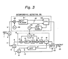
- Fig. 3 illustrates a third embodiment of the present invention.
- the interference detector employs a multiplexer composed of a plurality of narrow-band BPFs of different center frequencies and has a circuit arrangement in which the outputs of bands divided by the multiplexer are detected and converted into digital voltage values, which are processed by a CPU so as to detect an interference carrier and determine its frequency. Since the interference reducing circuit is identical in construction with those shown in Figs. 1 and 2, a description will be given only of the interference detector using the multiplexer.
- the IF signal applied to the input terminal 1 is applied via the hybrid circuit 2 to an interference detector 39.
- the IF signal fed to the interference detector 39 is converted by a local oscillator 46 and a MIX 40 into a signal of the operating frequency band of a multiplexer 41, thereafter being applied thereto for division into individual bands.
- the output terminal of each of a plurality of narrow band-pass BPFs forming the multiplexer 41 is connected to a detector and an A/D converter, and a digital voltage value A/D converted from an analog detected voltage of each band is stored into a memory of a CPU 43.
- the CPU 43 determines the presence or absence of an interference carrier in each band by digital processing following a predetermined algorithm based on a detected voltage value in the absence of an interference carrier. While in Fig.
- the CPU 43 applies a switch change-over signal to the switch 22, providing therethrough the output of the interference reducing circuit 12 to the output terminal 23. Where it is determined that no interference carrier exists, the CPU 43 controls the switch 22 so that the IF signal transmitted over the bypass transmission line 10 is provided intact to the output terminal 23.
- an interference reducing device which is characterized in that the attenuation of a band-elimination filter for reducing an interference carrier is limited to a value smaller than a certain one, or for frequency bands in which spectra are produced by bit sequence for burst signal demodulating use, the IF signal is combined with the band-elimination filter output via a narrow band-pass filter to limit the attenuation in these frequency bands to a value smaller than a certain one, thereby preventing the TDMA signal quality from being degraded by the insertion of the band-elimination filter in a particular frequency band.
- the IF input signal is passed intact through the interference reducing device; so that no deterioration of the signal quality is
- Fig. 4 illustrates a fourth embodiment of an interference wave eliminating circuit employing the interference detector of the present invention.
- An IF signal applied to an input terminal 101 is branched by a hybrid circuit 102 and provided to first and second lines 103 and 104.
- the IF signal on the first line 103 is applied to an interference detector 116, wherein it is used for detecting the presence or absence of an interference carrier and its frequency.
- the IF signal on the second line is branched by a hybrid circuit 105 into two, one of which is applied to an interference eliminating circuit 107 and the other of which is applied to an IF line 106.
- BEF band elimination filter
- the IF line 106 is a bypass transmission line for a normal IF signal containing no interference and is connected via a switch 114 to an output terminal 115.
- the interference eliminating circuit 107 is made up of a first mixer (MIX) 108, a band-elimination filter (BEF) 109 for eliminating a narrow-band interference carrier, a second mixer 111, a hybrid circuit 13 for branching a local oscillator signal for input into the first and second mixers, and band-pass filters (BPF) 110 and 112 each of which eliminates an image frequency components resulting from frequency conversion and permits the passage therethrough of only a desired signal band component.
- the interference elimination circuit 107 functions as a frequency-variable narrow-band elimination filter by changing the frequency of a voltage-controlled oscillator (VCO) 122 which is used as a local oscillator for each of the first and second mixers.
- VCO voltage-controlled oscillator
- An interference carrier mixed in the IF signal provided to the input terminal 101 is detected by the interference detector 116, and a VCO control signal and a switch change-over signal are yielded in search for the center frequency of the detected interference. Consequently, the IF signal provided to the interference eliminating circuit 107 is eliminated by the band-elimination filter 109 in the frequency band in which the interference exists. Upon detection of the interference eliminating circuit 107 changes over the switch 115 and provided therethrough at the output terminal 115 the IF signal having removed therefrom the interference band.
- the interference detector 116 in this embodiment comprises a third mixer 117, a multiplexer 118 employing two narrow-band filters of different center frequencies, A/D converters 119 and 120 for detecting the outputs of respective bands divided by the multiplexer 118 and converting them into digital voltage values, a CPU 124 for processing the digital values, a D/A converter 121 for controlling the oscillation frequency of the VCO 122 with the CPU output, the VCO 122, and a hybrid circuit 123 for branching the VCO output.
- the IF signal applied to the interference detector 116 is converted by the VCO 122 and the mixer 117 into the operating frequency band of the multiplexer 118 and is then applied to the multiplexer 118, wherein its band is divided into plural parts.
- Each of the two narrow-band filters forming the multiplexer 118 is connected at its output terminal to a detector and the A/D converter, and a digital version of the analog detected voltage of each divided band is loaded into a memory of the CPU 124.
- the CPU 124 sweeps the VCO 122 and performs digital processing following an algorithm determined on the basis of a voltage value detected in the absence of an interference in the desired signal band, thereby deciding the presence or absence of an interference wave in each band being swept. Where it is determined by such digital processing that an interference is present in a certain frequency band, the sweep of the VCO 122 is stopped and the output levels of the multiplexer 118 are compared with one another in terms of magnitude to follow up the interference.
- Fig. 5 shows frequency vs. detected level relationships obtained when a signal component containing an interference was detected by a multiplexer having an arrangement in which narrow-band filters BPF-1 and BPF-2 of center frequencies f1 and f2 were disposed so that they would cross each other at a point of a 3 dB passage loss.
- the VCO by sweeping the VCO and comparing the detected level of the multiplexer 118 in the band of the signal frequency-converted by the mixer 117 with the detected level obtained in the absence of the interference, or by setting a threshold value at a point higher than the detected level of the signal component, it is possible to decide the presence or absence of the interference and estimate its frequency from the sweep frequency of the VCO. Further, as regards the follow-up of the interference carrier frequency when it varies, the direction of its change can be decided by comparing the detected levels of the filters BPF-1 and BPF-2 with each other in terms of magnitude. The accuracy of estimation of the interference carrier frequency could be increased by forming the multiplexer with more than two band-pass filters.
- Fig. 6 illustrates a fifth embodiment of the present invention.
- the interference wave detecting sensitivity is high when the pass bandwidth of the multiplexer is small, but in this instance, the speed for sweeping the signal band is limited.
- an increase in the pass bandwidth of the multiplexer 118 will raise the sweep speed but will lower the accuracy of estimation of the interference carrier frequency as well as the detecting sensitivity.
- This embodiment is adapted to solve these short-comings by forming the interference detector with circuits which possess the detecting function and the follow-up function, respectively.
- the input signal line to the interference detector is branched into two, both of which are connected circuits which are of the same construction as that of the interference detector 116 used in the first embodiment and are operated as a follow-up circuit 116 a and a detecting circuit 26, respectively.
- Multiplexers used in the follow-up circuit 116 a and the detecting circuit 26 have different pass bandwidths.
- the multiplexer employing a band-pass filter of a large bandwidth is used to detect the interference wave which the multiplexer employing a band-pass filter of a small bandwidth is used to follow up the interference carrier, thereby speeding up the detection of the interference and permitting highly accurate follow-up of its carrier frequency.
- the detecting circuit in this embodiment comprises a mixer 127, a multiplexer 128 employing a plurality of narrow band-pass filters, A/D converters 129 and 130 for detecting the outputs of bands divided by the multiplexer 128 and converting them into digital voltage values, a CPU 124 for processing these digital values, a D/A converter 131 for controlling the oscillation frequency of a VCO 132 with the output of the CPU 124, and the VCO 132.
- the IF signal applied to the input signal terminal 101 is branched by the hybrid circuits 102 and 105, from which the branched parts are applied to the interference eliminating circuit 107, the IF line 106 and the interference detector is branched by a hybrid circuit 125, from which the branched parts are provided to the interference detecting circuit 126 and the follow-up circuit 116 a .
- the IF signal fed to the detecting circuit 126 is converted into the operating frequency band of the multiplexer 128 by means of the VCO 132 and the mixer 127, thereafter being applied to the multiplexer 128.
- a digital voltage value converted from an analog voltage value which is the detected output of the multiplexer 128 is loaded into a memory of the CPU 124.
- the CPU 124 sweeps the VCO 132 and performs digital processing following an algorithm determined on the basis of a voltage value detected in the absence of an interference carrier in the desired signal band, thereby deciding the presence or absence of an interference carrier in each band being swept.
- the sweep of the VCO 132 is stopped and the output levels of the multiplexer 128 are compared with each other in terms of magnitude to obtain the center frequency of the interference carrier so that the oscillation frequency of the VCO 132 of the follow-up circuit 116 a is controlled via the CPU 124 accordingly.
- the follow-up circuit 116 a is identical in construction with the interference detector 116 in the embodiment shown in Fig. 4, and the frequency of the VCO 122 is set by control of the CPU 124 based on information of the detecting circuit 124.
- the output of the VCO 122 which follows up the varying frequency is output to the interference eliminating circuit 107.
- the CPU 124 sends a switch change-over signal to the switch 114, through which the IF signal applied to the interference eliminating circuit 107 is provided to the output terminal 115.
- the CPU 124 allows the IF signal on the IF line 106 to be provided intact to the output terminal 115.
- the interference reducing device of the present invention affords reduction of a narrow-band, high-power-density interference carrier which suddenly gets mixed into the satellite circuit, and hence prevents degradation of the circuit quality of the digital satellite communication system, in particular, prevents system down by the interference in the TDMA system.
- the interference detector of the present invention can quickly detect a narrow-band interference carrier which suddenly gets mixed into a satellite circuit and to obtain an output frequency of a voltage-controlled oscillator which follows up the interference wave with high accuracy.
Landscapes
- Engineering & Computer Science (AREA)
- Computer Networks & Wireless Communication (AREA)
- Signal Processing (AREA)
- Noise Elimination (AREA)
Abstract
Description
- The present invention relates to an interference reducing device which detects and reduces unmodulated carriers, narrow-band FM carriers, or their sweep carriers which get mixed as interference carriers into the communication band in a TDMA (Time Division Multiple Access) digital satellite communication system.
- With the development of satellite communication systems, the number of earth stations which access the same satellite is on the increase. Occasionally the situation arises where non-modulated carriers, narrow-band FM carriers, or their sweep carriers are emitted as unwanted carriers owing to a fault or operation mistake of earth station equipment. In the TDMA system each station transmits, every fixed period of time called a TDMA frame, a burst-like TDMA signal of a fixed carrier frequency within a certain time slot allotted to the station. To establish burst synchronization for high precision control of the burst transmission timing of respective stations to ensure that they send their bursts at different timing, a reference station sends a reference burst for each TDMA frame. The reference burst is used for system control as well as for maintaining the synchronization of the TDMA system. On the other hand, a traffic station for transmitting and receiving information sends a traffic burst. The application of the above-mentioned unwanted carriers as interference carriers to the TDMA system not only degrades the signal quality but also may sometimes hinder the system control by the reference burst and synchronization of the traffic burst, making communication impossible throughout the system.
- In the time division multiple access system (the TDMA system) introduced in the digital satellite communication, each station transmits a burst-like TDMA signal of a fixed carrier frequency within a certain time slot allotted to the station. To establish burst synchronization for high precision control of the burst transmission timing of respective stations so that they send their bursts at different timing, a synchronization burst is inserted for each TDMA frame. The synchronization burst (a reference burst) sent from a reference station is employed for system control as well as for maintaining the synchronization of the TDMA system. An interference carrier, if mixed in such a communication system, will degrade the signal quality and, further, may sometimes destroy the burst synchronization and the system control by the reference burst, leading to a failure in communication.
- For detecting an interference carrier mixed in the input signal band, there has been proposed a method which obtains the interference carrier frequency from the output frequency of a voltage-controlled oscillator which is synchronized with the narrow-band interference carrier by means of a phase lock loop, or a method in which the input signal band is divided by a filter multiplexer composed of a plurality of narrow band-pass filters of different center frequencies and a signal component in each divided band is detected, converted into a digital value and processed by a CPU for estimating the interference wave carrier frequency. The interference detector employing the phase lock loop is simple in circuit construction and permits easy detection and follow-up of a unmodulated carrier or interference carrier which continuously sweeps in the received signal band, but in the case where the interference carrier mixed in the input signal is discontinuous or intermittent, synchronization of the phase lock loop cannot be maintained. Further, when the level of the interference carrier becomes low, the synchronized state of the phase lock loop becomes unstable, making it difficult to decide the presence or absence of the interference carrier. On the other hand, the filter multiplexer system is capable of detecting an interference carrier, even if it is discontinuous or intermittent, but in a case of detecting an interference carrier of power lower than that of the input signal, it is necessary to use a filter multiplexer of enhanced detecting sensitivity by dividing a desired transmission band with a number of narrow-band filters, a number of A/D converters for converting the detected outputs of the multiplexer into digital values and a CPU of high-speed operation. This inevitably makes the interference detector bulky and expensive.
- An object of the present invention is to provide an interference reducing device which, based on the fact that the modulated carrier for use in the digital satellite communication system and the narrow-band interference carrier are, in general, markedly different from each other in power density, quickly detects the narrow-band interference carrier which suddenly gets mixed into the input signal band and, eliminates that one portion of the signal frequency band in which the interference carrier exists, through use of a band-rejection filter, thereby preventing degradation of the line quality in the TDMA system owing to the interference carrier and precluding the possibility of system down.
- Another object of the present invention is to provide an interference detector of a multiplexer sweep system which obviates the above-mentioned defects of the prior art by combining the functions of the phase lock loop and the filter multiplexer and permits the estimation of the frequency of an interference carrier with a relatively simple structure.
- For rapid and accurate detection of the interference carrier frequency mixed in the input signal band, it is possible to employ a system which derives the interference carrier frequency from the output frequency of a voltage controlled oscillator (VCO) synchronized with the narrow-band interference carrier by means of a phase-lock loop, or a system which divides the input signal band by a filter multiplexer composed of a number of narrow band-pass filters of different center frequencies and estimates the interference carrier frequency by detecting a signal component in each divided band. The interference carrier frequency mixed in the input signal band is thus detected and a certain band in which the interference carrier exists is rejected by a band-elimination filter. In the TDMA system, however, since each station needs to perform, at high speed, a carrier regeneration and a bit timing regeneration for the demodulation of the received burst, the bursts which are transmitted from the reference station and the traffic stations are each headed by carrier and bit timing recovery sequence. These bit sequences are often composed of an unmodulated carrier and a periodic repetition pattern for high-speed synchronization, and their frequency spectra concentrate at a particular frequency. For example, in an INTELSAT TDMA system which utilizes a 120 Mbps four-phase phase-shift keying modulation (QPSK), the carrier and bit timing recovery sequence are each composed of an unmodulated wave and a repetition pattern of 0/π, and hence the frequency spectrum during the sending of the bit string centers on the center frequency f0 of the signal band and a frequency f0±30MHz. Thus, if the spectra in particular frequency ranges by the bit sequence are rejected by the band-rejection filter, then the carrier recovery and the bit timing recovery cannot be achieved, and consequently, no normal demodulation is feasible. On the other hand, since randomly modulated frequency spectra are partly rejected outside these frequency ranges, the influence of removal of signal components by the band-elimination filter is slight. The amount of the narrow-band interference carrier reduced by the band-elimination filter in the TDMA system differs with the configurations of the bit sequence for carrier and bit timing recovery.
- According to the present invention, when an interference carrier is reduced by processing a signal of an input frequency to a demodulator such as a PSK signal appended with bit sequence for carrier recovery and bit timing recovery for use in the TDMA system, for example, a signal of the intermediate frequency (IF) band of a 140 MHz center frequency, the attenuation of a band-elimination filter is limited to a value smaller than a certain one, or for the frequency bands in which spectra are produced by the bit sequence, the IF signal is combined with the band-elimination filter output via a narrow band-pass filter to control the attenuation in each of these frequency bands to a value smaller than a certain one, thereby preventing the signal quality of the TDMA signal from being degraded by the insertion of the band-elimination filter. When no interference wave is detected, the input IF signal is passed intact through the interference reducing device so that no deterioration of the signal quality will be introduced by the reducing device.
- To attain the above second object, the interference detector of the present invention has such a construction as follows:
- The interference detector comprises: a frequency converter employing a voltage-controlled oscillator as a local oscillator; a multiplexer employing a plurality of narrow band-pass filters of center frequencies set within the output frequency band of the frequency converter; a circuit for detecting and converting the output of the multiplexer into a digital voltage value; a CPU for processing the converted digital voltage value; a D/A converter for controlling the oscillation frequency of the voltage-controlled oscillator with the CPU output; and means responsive to a control signal from the CPU to sweep the oscillation frequency of the voltage-controlled oscillator, to apply a desired frequency-converted input signal band component to the multiplexer and to detect and convert its output into a digital voltage value for input into the CPU.
- Based on the fact that a digital modulated signal and a narrow-band interference carrier mixed therein sharply differ from each other in power density, the interference detector of the present invention decides the presence or absence of the interference carrier, its frequency and the direction of its change by processing in the CPU and follows up the interference carrier frequency to obtain an oscillation frequency of the voltage-controlled oscillator which is equal to the interference carrier frequency.
- The detecting speed is in proportion to the pass bandwidth of the multiplexer using a plurality of band-pass filters, but the follow-up accuracy is in reverse proportion to the above-said pass bandwidth. By using a multiplexer of a large pass bandwidth to increase the detecting speed of the interference detector and by using a multiplexer of a relatively small bandwidth to enhance the follow-up accuracy of an interference follow-up circuit, it is possible to drive the voltage-controlled oscillator at a frequency following the interference carrier frequency.
- The present invention will be described in detail below with reference to the accompanying drawings, in which:
- Fig. 1 is a block diagram illustrating an embodiment of the interference reducing device of the present invention;
- Figs. 2 and 3 are block diagram illustrating specific operative examples of an interference detector for use in the device depicted in Fig. 1;
- Figs. 4 and 6 are block diagrams illustrating embodiments of the interference detector of the present invention;
- Fig. 5 is a graph explanatory of the operation of this invention device.
- With reference to Fig. 1, a first embodiment of the interference reducing device according to the present invention will first be described. An IF signal applied to an input terminal 1 is branched by hybrid circuits (H) 2 and 5 and provided on first, second, third and
fourth lines first line 3 is applied to an interference detector 11 for detecting the presence or absence of an interference carrier and its frequency. The IF signal on thethird line 6 is applied to aninterference reducing circuit 12, in which, when an interference wave is detected, the signal frequency band where its frequency exists is reduced by a band-elimination filter (BEF) 14. Thefourth line 7 is further branched by ahybrid circuit 8 into fifth andsixth lines fifth line 9 is applied to ahybrid circuit 18 via a plurality of narrow band-pass filters 21 each of which uses, as its center frequency, a particular frequency at which spectra are produced by the afore-mentioned bit sequence in the IF band. In thehybrid circuit 18 the output of thefifth line 9 is combined with the output of thethird line 6 provided with the BEF 14. Thesixth line 10 is a bypass transmission line of the IF signal in the normal state where no interference is present, and this bypass is connected via aswitch 22 to anoutput terminal 23. - The
interference reducing circuit 12 comprises a first mixer (MIX) 13, thenarrow BEF 14 for interference wave reduction use, asecond mixer 16, ahybrid circuit 19 for branching the output of a local oscillator (VCO) 20 for application to the first andsecond mixers wave reducing circuit 12 the IF signal and the output of the voltage controlled oscillator (VCO) 20 used as a local oscillator are provided to themixer 13 to obtain a signal component of their sum (or difference) frequency, which is applied via theBEF 14 and theBPF 15 to theMIX 16 for conversion into a frequency of the difference (or sum) between it and the output frequency of theVCO 20, i.e. an IF signal. If the center frequency of theBEF 14 is selected within the output frequency band of theMIX 13, then the section between the input of theMIX 13 and the output of theMIX 16 can be used as a frequency variable narrow band-elimination filter by changing the oscillation frequency of theVCO 20. - When an interference carrier gets mixed into the IF signal applied to the input terminal 1 of this device, it is detected by the interference detector 11, which obtains its center frequency and then yields a VCO control signal and a switch change-over signal. The VCO control signal controls the oscillation frequency of the
VCO 20 so that the band-elimination frequency of theinterference reducing circuit 12 coincides with the frequency of the interference carrier. Accordingly, the IF signal provided on thethird line 6 is reduced by theBEF 14 of theinterference reducing circuit 12 in the frequency band in which the signal component is included and the interference carrier is present. To permit demodulation of the TDMA signal even in a case where the particular frequency band in which spectra are produced by the bit sequence appended to the burst signal is reduced by the band-elimination filter, it is necessary to limit the attenuation of the filter. However, this lessens the interference reducing effect. To heighten the interference reducing effect by removing the above-mentioned particular frequency band, the plurality ofnarrow BPFs 21, each using as its center frequency the particular frequency dependent on the configuration of the bit sequence, are connected to thefifth line 9, the outputs of theBPFs 21 are combined with the output of theinterference reducing circuit 12 by thehybrid circuit 18, and the attenuation of eachBPF 21 is adjusted. The attenuation of these frequency bands can thus be controlled. Incidentally, the interference detector 11 changes over theswitch 22 in accordance with the detection or nondetection of the interference and connects the interference band reducing output or the output of thesixth line 10 as the bypass transmission line to theoutput terminal 23. - Fig. 2 illustrates a second embodiment of the present invention. This embodiment employs a phase lock loop as the interference detector but the interference reducing circuit and the switch are exactly identical in construction to those in Fig. 1; so that the following description will be given mainly of the construction and the operation of the interference detector.
- The interference detector in this embodiment is divided into an
interference band extractor 24 which is composed of athird MIX 26, afourth MIX 28, aBPF 27 interposed between them and ahybrid circuit 29 for branching a local oscillation signal, and a phase synchronizing circuit (phase-lock loop) 25. Theinterference band extractor 24 has the same construction as theinterference reducing circuit 12 in the first embodiment and functions as a frequency variable type BPF by varying the frequency of a local oscillator. The pass-band width of theBPF 27 in theinterference band extractor 24 is set to about 10% of a desired signal band width so as to facilitate the interference pull-in operation of the phase-lock loop 25 which raises the interference carrier power vs. signal power ratio when an interference carrier gets mixed. The local oscillation signal to the third and fourth MIXs 26 and 28 is the output of aVCO 32 of the phase-lock loop 25 which is applied thereto viahybrid circuits local oscillator 35 and aMIX 34. - The phase synchronizing circuit (phase-lock loop) 25 is basically formed by a
phase detector 30, a low-pass filter (LPF) 31 and theVCO 32. In the normal state in which no interference is present, that is, when no phase synchronization is established, the oscillation frequency of theVCO 32 is controlled by the output voltage of asweep oscillator 37 and sweeps in the transmission band of a desired signal. The output of theVCO 32 is used also as the local oscillation signal source of theinterference band extractor 24. While no interference wave is detected, the transmission band of the desired signal is swept by theinterference band extractor 24 and the output having extracted a portion of the signal band is applied to the phase-lock loop 25 to hunt for the interference. - On the other hand, when the phase-
lock loop 25 is synchronized with the interference carrier, a synchronizationestablishment decision circuit 33 provides a control signal to anoutput control circuit 38 of thesweep oscillator 37, controlling theVCO 32 by the output voltage of theLPF 31 alone. Accordingly, the phase-lock loop 25 forms an ordinary phase locked loop which receives an interference carrier as its input signal and provides the output frequency of theVCO 32 synchronized with the interference carrier. The synchronizationestablishment decision circuit 33 decides whether or not the phase-lock loop 25 is synchronized with the interference carrier, and determines the detection or non-detection of the interference carrier. Upon detection of the interference carrier, the synchronizationestablishment decision circuit 33 changes over theswitch 22, through which the output of theinterference reducing circuit 12 is applied to theoutput terminal 23. As is the case with theinterference band extractor 24, the local oscillation frequency of theinterference reducing circuit 12 is provided by frequency converting the oscillation frequency of theVCO 32 with thelocal oscillator 35 and theMIX 34 and then branching the converted output with ahybrid circuit 36. - Fig. 3 illustrates a third embodiment of the present invention. In this embodiment the interference detector employs a multiplexer composed of a plurality of narrow-band BPFs of different center frequencies and has a circuit arrangement in which the outputs of bands divided by the multiplexer are detected and converted into digital voltage values, which are processed by a CPU so as to detect an interference carrier and determine its frequency. Since the interference reducing circuit is identical in construction with those shown in Figs. 1 and 2, a description will be given only of the interference detector using the multiplexer.
- The IF signal applied to the input terminal 1 is applied via the
hybrid circuit 2 to aninterference detector 39. The IF signal fed to theinterference detector 39 is converted by alocal oscillator 46 and aMIX 40 into a signal of the operating frequency band of amultiplexer 41, thereafter being applied thereto for division into individual bands. The output terminal of each of a plurality of narrow band-pass BPFs forming themultiplexer 41 is connected to a detector and an A/D converter, and a digital voltage value A/D converted from an analog detected voltage of each band is stored into a memory of aCPU 43. TheCPU 43 determines the presence or absence of an interference carrier in each band by digital processing following a predetermined algorithm based on a detected voltage value in the absence of an interference carrier. While in Fig. 3 only one CPU is shown to be used, it is also possible to perform parallel processing for respective bands through use of a plurality of CPUs for high-speed operation. In a case where it is determined by such digital processing that an interference carrier is present in a certain frequency band, information about the center frequency of the interference carrier is sent via D/A converter 44 from theCPU 43 to aVOC 45, from which a continuous wave corresponding to the center frequency of the interference carrier is provided to theinterference reducing circuit 12. In theinterference reducing circuit 12 theBEF 14 reduces the frequency band in which there exists the interference carrier containing the signal component of the IF signal applied to theinterference reducing circuit 12 via theinput terminal 12 and thehybrid circuit CPU 43 applies a switch change-over signal to theswitch 22, providing therethrough the output of theinterference reducing circuit 12 to theoutput terminal 23. Where it is determined that no interference carrier exists, theCPU 43 controls theswitch 22 so that the IF signal transmitted over thebypass transmission line 10 is provided intact to theoutput terminal 23. - With the above-described operation, when it is determined that an interference carrier is present in the IF input signal, a signal with the interference band reduced is output, whereas when it is determined that no interference carrier exists, the IF input signal is output intact. According to the present invention, it is possible to implement an interference reducing device which is characterized in that the attenuation of a band-elimination filter for reducing an interference carrier is limited to a value smaller than a certain one, or for frequency bands in which spectra are produced by bit sequence for burst signal demodulating use, the IF signal is combined with the band-elimination filter output via a narrow band-pass filter to limit the attenuation in these frequency bands to a value smaller than a certain one, thereby preventing the TDMA signal quality from being degraded by the insertion of the band-elimination filter in a particular frequency band. Incidentally, when no interference is detected, the IF input signal is passed intact through the interference reducing device; so that no deterioration of the signal quality is caused by the interference reducing device.
- Fig. 4 illustrates a fourth embodiment of an interference wave eliminating circuit employing the interference detector of the present invention. An IF signal applied to an input terminal 101 is branched by a
hybrid circuit 102 and provided to first andsecond lines first line 103 is applied to aninterference detector 116, wherein it is used for detecting the presence or absence of an interference carrier and its frequency. The IF signal on the second line is branched by ahybrid circuit 105 into two, one of which is applied to aninterference eliminating circuit 107 and the other of which is applied to an IFline 106. Upon detection of an interference, the signal frequency band in which the interference carrier frequency exists is eliminated by a band elimination filter (BEF) 109. TheIF line 106 is a bypass transmission line for a normal IF signal containing no interference and is connected via aswitch 114 to anoutput terminal 115. - The
interference eliminating circuit 107 is made up of a first mixer (MIX) 108, a band-elimination filter (BEF) 109 for eliminating a narrow-band interference carrier, a second mixer 111, ahybrid circuit 13 for branching a local oscillator signal for input into the first and second mixers, and band-pass filters (BPF) 110 and 112 each of which eliminates an image frequency components resulting from frequency conversion and permits the passage therethrough of only a desired signal band component. Theinterference elimination circuit 107 functions as a frequency-variable narrow-band elimination filter by changing the frequency of a voltage-controlled oscillator (VCO) 122 which is used as a local oscillator for each of the first and second mixers. An interference carrier mixed in the IF signal provided to the input terminal 101 is detected by theinterference detector 116, and a VCO control signal and a switch change-over signal are yielded in search for the center frequency of the detected interference. Consequently, the IF signal provided to theinterference eliminating circuit 107 is eliminated by the band-elimination filter 109 in the frequency band in which the interference exists. Upon detection of theinterference eliminating circuit 107 changes over theswitch 115 and provided therethrough at theoutput terminal 115 the IF signal having removed therefrom the interference band. - The
interference detector 116 in this embodiment comprises athird mixer 117, amultiplexer 118 employing two narrow-band filters of different center frequencies, A/D converters multiplexer 118 and converting them into digital voltage values, aCPU 124 for processing the digital values, a D/A converter 121 for controlling the oscillation frequency of theVCO 122 with the CPU output, theVCO 122, and ahybrid circuit 123 for branching the VCO output. - The IF signal applied to the
interference detector 116 is converted by theVCO 122 and themixer 117 into the operating frequency band of themultiplexer 118 and is then applied to themultiplexer 118, wherein its band is divided into plural parts. Each of the two narrow-band filters forming themultiplexer 118 is connected at its output terminal to a detector and the A/D converter, and a digital version of the analog detected voltage of each divided band is loaded into a memory of theCPU 124. TheCPU 124 sweeps theVCO 122 and performs digital processing following an algorithm determined on the basis of a voltage value detected in the absence of an interference in the desired signal band, thereby deciding the presence or absence of an interference wave in each band being swept. Where it is determined by such digital processing that an interference is present in a certain frequency band, the sweep of theVCO 122 is stopped and the output levels of themultiplexer 118 are compared with one another in terms of magnitude to follow up the interference. - Next, a detailed description will be given of the detection follow-up operation of the interference detector employing the
multiplexer 118 formed by two narrow band-pass filters. - Fig. 5 shows frequency vs. detected level relationships obtained when a signal component containing an interference was detected by a multiplexer having an arrangement in which narrow-band filters BPF-1 and BPF-2 of center frequencies f1 and f2 were disposed so that they would cross each other at a point of a 3 dB passage loss. By selecting the pass bandwidths of filters BPF-1 and BPF-2 sufficiently small as compared with the signal band, the difference between a detected level PS of a signal component of varying power density and a detected level P1 or P2 in the presence of an interference increases, making it possible to detect the interference with high sensitivity. Thus, by sweeping the VCO and comparing the detected level of the
multiplexer 118 in the band of the signal frequency-converted by themixer 117 with the detected level obtained in the absence of the interference, or by setting a threshold value at a point higher than the detected level of the signal component, it is possible to decide the presence or absence of the interference and estimate its frequency from the sweep frequency of the VCO. Further, as regards the follow-up of the interference carrier frequency when it varies, the direction of its change can be decided by comparing the detected levels of the filters BPF-1 and BPF-2 with each other in terms of magnitude. The accuracy of estimation of the interference carrier frequency could be increased by forming the multiplexer with more than two band-pass filters. - Fig. 6 illustrates a fifth embodiment of the present invention. In a case of detecting and following up an interference carrier by sweeping, the
filter multiplexer 118 of theinterference detector 116 in the first embodiment of the invention, the interference wave detecting sensitivity is high when the pass bandwidth of the multiplexer is small, but in this instance, the speed for sweeping the signal band is limited. On the other hand, an increase in the pass bandwidth of themultiplexer 118 will raise the sweep speed but will lower the accuracy of estimation of the interference carrier frequency as well as the detecting sensitivity. This embodiment is adapted to solve these short-comings by forming the interference detector with circuits which possess the detecting function and the follow-up function, respectively. In this embodiment the input signal line to the interference detector is branched into two, both of which are connected circuits which are of the same construction as that of theinterference detector 116 used in the first embodiment and are operated as a follow-up circuit 116a and a detectingcircuit 26, respectively. Multiplexers used in the follow-up circuit 116a and the detectingcircuit 26 have different pass bandwidths. The multiplexer employing a band-pass filter of a large bandwidth is used to detect the interference wave which the multiplexer employing a band-pass filter of a small bandwidth is used to follow up the interference carrier, thereby speeding up the detection of the interference and permitting highly accurate follow-up of its carrier frequency. - Now, a description will be given, with reference to Fig. 6, of the construction and operation of the fifth embodiment of the invention.
- The detecting circuit in this embodiment comprises a
mixer 127, amultiplexer 128 employing a plurality of narrow band-pass filters, A/D converters multiplexer 128 and converting them into digital voltage values, aCPU 124 for processing these digital values, a D/A converter 131 for controlling the oscillation frequency of aVCO 132 with the output of theCPU 124, and theVCO 132. - The IF signal applied to the input signal terminal 101 is branched by the
hybrid circuits interference eliminating circuit 107, theIF line 106 and the interference detector is branched by ahybrid circuit 125, from which the branched parts are provided to theinterference detecting circuit 126 and the follow-up circuit 116a. The IF signal fed to the detectingcircuit 126 is converted into the operating frequency band of themultiplexer 128 by means of theVCO 132 and themixer 127, thereafter being applied to themultiplexer 128. - A digital voltage value converted from an analog voltage value which is the detected output of the
multiplexer 128 is loaded into a memory of theCPU 124. TheCPU 124 sweeps theVCO 132 and performs digital processing following an algorithm determined on the basis of a voltage value detected in the absence of an interference carrier in the desired signal band, thereby deciding the presence or absence of an interference carrier in each band being swept. In a case where it is determined by such digital processing that an interference carrier is present in a certain frequency band, the sweep of theVCO 132 is stopped and the output levels of themultiplexer 128 are compared with each other in terms of magnitude to obtain the center frequency of the interference carrier so that the oscillation frequency of theVCO 132 of the follow-up circuit 116a is controlled via theCPU 124 accordingly. The follow-up circuit 116a is identical in construction with theinterference detector 116 in the embodiment shown in Fig. 4, and the frequency of theVCO 122 is set by control of theCPU 124 based on information of the detectingcircuit 124. In a case where the interference carrier frequency is varying, the output of theVCO 122 which follows up the varying frequency is output to theinterference eliminating circuit 107. Moreover, theCPU 124 sends a switch change-over signal to theswitch 114, through which the IF signal applied to theinterference eliminating circuit 107 is provided to theoutput terminal 115. When it is determined that no interference is present, theCPU 124 allows the IF signal on theIF line 106 to be provided intact to theoutput terminal 115. - It is also possible to omit the D/
A converter 131 and theVCO 132 in the detectingcircuit 126 by branching the output of theVCO 122 of the follow-up circuit 116a for input into themixer 127 and by modifying the control sequence of theCPU 124 which accompanies the interference detecting and following-up operations. - As described above in detail, the interference reducing device of the present invention affords reduction of a narrow-band, high-power-density interference carrier which suddenly gets mixed into the satellite circuit, and hence prevents degradation of the circuit quality of the digital satellite communication system, in particular, prevents system down by the interference in the TDMA system.
- It is possible with the interference detector of the present invention to quickly detect a narrow-band interference carrier which suddenly gets mixed into a satellite circuit and to obtain an output frequency of a voltage-controlled oscillator which follows up the interference wave with high accuracy.
Claims (7)
- A narrow-band interference reducing device:
wherein a received signal path is branched into first and second lines, said first line having an interference detector for detecting a narrow-band interference carrier mixed in a digital modulated signal;
wherein said second line is branched into third and fourth lines, said third line having first and second mixers and a narrow-band elimination filter and a band-pass filter connected both between said first and second mixers, said band-pass filter permitting the passage therethrough of only a desired frequency-converted signal band component;
wherein the output of a voltage-controlled oscillator whose oscillation frequency is controlled by the output of said interference detector is applied as local oscillator outputs of said first and second mixers to thereby control the center frequency for band elimination between the input and output of said third line;
wherein said fourth line is branched into fifth and sixth lines, said fifth line having a plurality of narrow band-pass filters whose transmission losses are set to a fixed value and whose center frequencies are particular frequencies within the band of a received signal; and
wherein means is provided for combining the output of said third line having said band elimination filter and the output of said fifth line having said narrow band-pass filters. - An interference reducing device:
wherein a received signal path is branched into first and second lines, said first line having an interference detector for detecting a narrow band interference carrier mixed in a digital modulated signal;
wherein said second line is branched into third and fourth lines, said third line having first and second mixers and a narrow band-elimination filter and a band-pass filter both connected between said first and second mixers, said narrow-band elimination filter having its attenuation at the center frequency set to a fixed value and said band-pass filter permitting the passage therethrough of only a desired frequency-converted signal band component;
wherein means is provided whereby the output of a voltage-controlled oscillator whose oscillation frequency is controlled by the output of said interference detector is applied as local oscillator outputs of said first and second mixers; and
wherein the center frequency for band elimination between the input and output of said third line is controlled by the output frequency of said voltage-controlled oscillator and the attenuation of the interference carrier by said band-elimination filter is limited to a fixed value. - An interference reducing device according to claim 1 or 2, wherein said interference detector is formed by a phase-lock loop which is synchronized with an input interference carrier, and wherein the elimination frequency of said interference reducing circuit is controlled by the output frequency of a voltage-controlled oscillator of said phase-lock loop.
- An interference reducing circuit according to claim 1 or 2, wherein said interference detector is formed by a multiplexer composed of a plurality of narrow band-pass filters of different center frequencies and a circuit for detecting and converting each output of said multiplexer into a digital voltage value, and wherein an input signal band is divided by said multiplexer and a detected voltage value of each divided band is processed to thereby detect the interference carrier and control the oscillation frequency of said voltage-controlled oscillator.
- An interference detector for a narrow-band interference eliminating circuit in which a narrow-band filter and a band-pass filter which permits the passage therethrough of only desired frequency-converted signal band components are connected between first and second mixers, and the output of a voltage-controlled oscillator, whose oscillation frequency is controlled by the output of an interference detecting circuit for detecting a narrow-band interference carrier mixed in a digital modulated signal input thereto as an input signal, is provided as the local oscillator output of each of said first and second mixers to thereby control the center frequency of the elimination band of said band-elimination filter, said interference detector comprising:
a third mixer; a multiplexer employing a plurality of narrow band-pass filters; a circuit for detecting and converting the output of said multiplexer into a digital voltage value; a CPU for processing the detected digital voltage value; a D/A converter for controlling the oscillation frequency of said voltage-controlled oscillator with the output of said CPU; and means whereby said input signal is frequency-converted by applying it to said third mixer employing said voltage-controlled oscillator as its local oscillator and the output of said multiplexer having its center frequency set in said frequency-converted desired signal band is detected and converted into a digital voltage value for input into said CPU;
wherein the oscillation frequency of said voltage-controlled oscillator is swept by a control signal from said CPU, digital voltage values of plural outputs of said multiplexer swept in a desired signal band are processed by said CPU, whereby the presence or absence of said interference carrier, its frequency and the direction of its change are decided to permit said interference carrier to be followed. - An interference wave detector according to claim 5, which further comprises a second line branched from a first input signal line, siad second line having a circuit made up of a fourth mixer, a second multiplexer employing a plurality of narrow band-pass filters of pass bandwidths larger than that of said narrow band-pass filter connected to said first line, a circuit for detecting and converting the output of said second multiplexer into a digital voltage value, a CPU for processing the detected digital voltage value, and a D/A converter for controlling the oscillation frequency of said second voltage-controlled oscillator with the output of said CPU;
wherein the oscillation frequency of said second voltage-controlled oscillator is swept by a control signal from said second-mentioned CPU, the digital voltage value of the output of said second multiplexer swept in a desired signal band is processed by said CPU to decide the presence or absence of said interference carrier and its frequency, the oscillation frequency of the voltage-controlled of said first line is controlled by said CPU and digital voltage values of plural outputs of the multiplexer of said first line are processed by said CPU to decide the direction of change of the interference carrier frequency and follow it up, whereby said interference carrier can be quickly detected and the output frequency of said voltage-controlled oscillator of said first line following the interference carrier frequency with high accuracy can be output. - An interference detector according to claim 6, wherein the voltage-controlled oscillator of said first line is used as a local oscillator of said fourth mixer connected to said second line, the oscillation frequency of said voltage-controlled oscillator is swept with a control signal from said CPU, the digital voltage value of the output of said second multiplexer swept in a desired signal band is processed by said processor to decide the presence or absence of the interference carrier and its frequency, and after the detection of the interference carrier, the digital voltage value of the output of said multiplexer connected to said first line is processed by said CPU to decide the direction of change of the interference carrier frequency to be followed, whereby the interference can be quickly detected and the output frequency of said voltage-controlled oscillator connected to said first line following the interference carrier frequency with high accuracy can be output.
Priority Applications (1)
| Application Number | Priority Date | Filing Date | Title |
|---|---|---|---|
| EP95101367A EP0651519B1 (en) | 1990-02-07 | 1990-12-07 | Interference detector |
Applications Claiming Priority (5)
| Application Number | Priority Date | Filing Date | Title |
|---|---|---|---|
| JP26178/90 | 1990-02-07 | ||
| JP2026179A JP2561868B2 (en) | 1990-02-07 | 1990-02-07 | Interference wave detection circuit |
| JP26179/90 | 1990-02-07 | ||
| JP2026180A JP2581985B2 (en) | 1990-02-07 | 1990-02-07 | Interference wave canceller |
| JP2026178A JP2561867B2 (en) | 1990-02-07 | 1990-02-07 | Interference reduction device |
Related Child Applications (2)
| Application Number | Title | Priority Date | Filing Date |
|---|---|---|---|
| EP95101367A Division EP0651519B1 (en) | 1990-02-07 | 1990-12-07 | Interference detector |
| EP95101367.1 Division-Into | 1990-12-07 |
Publications (3)
| Publication Number | Publication Date |
|---|---|
| EP0440920A2 true EP0440920A2 (en) | 1991-08-14 |
| EP0440920A3 EP0440920A3 (en) | 1992-08-05 |
| EP0440920B1 EP0440920B1 (en) | 1995-11-15 |
Family
ID=27285292
Family Applications (1)
| Application Number | Title | Priority Date | Filing Date |
|---|---|---|---|
| EP90123570A Expired - Lifetime EP0440920B1 (en) | 1990-02-07 | 1990-12-07 | Interference detection and reduction |
Country Status (2)
| Country | Link |
|---|---|
| US (1) | US5222106A (en) |
| EP (1) | EP0440920B1 (en) |
Cited By (7)
| Publication number | Priority date | Publication date | Assignee | Title |
|---|---|---|---|---|
| EP0570166A1 (en) * | 1992-05-12 | 1993-11-18 | Hughes Aircraft Company | Interference detection and cancellation system and method |
| EP0704982A2 (en) * | 1994-09-30 | 1996-04-03 | AT&T Corp. | A radio receiver for processing a multi-carrier signal with a large dynamic range |
| US5933768A (en) * | 1997-02-28 | 1999-08-03 | Telefonaktiebolaget L/M Ericsson | Receiver apparatus, and associated method, for receiving a receive signal transmitted upon a channel susceptible to interference |
| WO2000005741A1 (en) * | 1998-07-20 | 2000-02-03 | Samsung Electronics Company, Limited | Multiple-channel digital receiver for global positioning system |
| EP0704992A3 (en) * | 1994-09-30 | 2000-05-24 | AT&T Corp. | Cellular communications system with multicarrier signal processing |
| WO2003014762A3 (en) * | 2001-08-08 | 2003-04-10 | Astrium Ltd | A signal separating system |
| WO2012000761A1 (en) * | 2010-06-28 | 2012-01-05 | Alcatel Lucent | Multicarrier receiver in a wireless telecommunication network |
Families Citing this family (25)
| Publication number | Priority date | Publication date | Assignee | Title |
|---|---|---|---|---|
| US5729755A (en) * | 1991-09-04 | 1998-03-17 | Nec Corporation | Process for transmitting data in a data processing system with distributed computer nodes, communicating via a serial data bus, between which data messages are exchanged, tested for acceptance in a computer node, and stored temporarily |
| US5974101A (en) * | 1992-04-28 | 1999-10-26 | Canon Kabushiki Kaisha | Spread spectrum modulation communication apparatus for narrow band interference elimination |
| US5325188A (en) * | 1992-05-14 | 1994-06-28 | Hitachi America, Ltd. | Apparatus for NTSC signal interference cancellation through the use of digital recursive notch filters |
| US5325204A (en) * | 1992-05-14 | 1994-06-28 | Hitachi America, Ltd. | Narrowband interference cancellation through the use of digital recursive notch filters |
| US5400084A (en) * | 1992-05-14 | 1995-03-21 | Hitachi America, Ltd. | Method and apparatus for NTSC signal interference cancellation using recursive digital notch filters |
| US5638407A (en) * | 1993-04-01 | 1997-06-10 | Mitsubishi Denki Kabushiki Kaisha | Inversion prevention device |
| US5430893A (en) * | 1993-08-11 | 1995-07-04 | At&T Corp. | Radio receiver with increased dynamic range |
| JPH07297900A (en) * | 1994-04-26 | 1995-11-10 | Mitsubishi Electric Corp | Communication equipment taking countermeasure against noise sound |
| US5694395A (en) * | 1994-09-30 | 1997-12-02 | Lucent Technologies, Inc. | Method and apparatus for processing multicarrier signals |
| US5570350A (en) * | 1994-09-30 | 1996-10-29 | Lucent Technologies Inc. | CDMA cellular communications with multicarrier signal processing |
| CN1501590A (en) | 1994-11-30 | 2004-06-02 | ���µ�����ҵ��ʽ���� | Receiving circuit |
| US5745846A (en) * | 1995-08-07 | 1998-04-28 | Lucent Technologies, Inc. | Channelized apparatus for equalizing carrier powers of multicarrier signal |
| US5757864A (en) * | 1995-08-17 | 1998-05-26 | Rockwell Semiconductor Systems, Inc. | Receiver with filters offset correction |
| JPH09162766A (en) * | 1995-12-04 | 1997-06-20 | Alps Electric Co Ltd | Satellite broadcasting reception tuner |
| US5949472A (en) * | 1996-12-10 | 1999-09-07 | Intel Corporation | Method and apparatus for tuning channels for CATV and television applications |
| US6057876A (en) * | 1996-12-18 | 2000-05-02 | General Instrument Corporation | Dual conversion settop terminal including a system for avoiding oscillator difference beats |
| TW391114B (en) * | 1997-01-31 | 2000-05-21 | Scientific Atlanta | System and method for harmonic interference avoidance in carrier recovery for digital demodulation |
| JP3729694B2 (en) | 1999-10-29 | 2005-12-21 | 富士通株式会社 | ADSL modem |
| US7016436B1 (en) * | 1999-12-17 | 2006-03-21 | Ericsson, Inc. | Selective joint demodulation systems and methods for receiving a signal in the presence of noise and interference |
| JP3836688B2 (en) * | 2001-05-25 | 2006-10-25 | 株式会社エヌ・ティ・ティ・ドコモ | Radio link interference detection method and interference prevention system |
| US20040057503A1 (en) * | 2002-09-24 | 2004-03-25 | Motorola, Inc. | Method and apparatus for processing a composite signal including a desired spread spectrum signal and an undesired narrower-band interfering signal |
| US7642910B2 (en) * | 2006-06-29 | 2010-01-05 | Honeywell International Inc. | Multi-frequency alarm system receiver with interference detection |
| WO2008054385A1 (en) * | 2006-11-01 | 2008-05-08 | Thomson Licensing | A co-channel interference remover |
| CN110442890B (en) * | 2018-05-04 | 2023-05-16 | 瑞昱半导体股份有限公司 | Circuit design system and inspection method |
| US20230208456A1 (en) * | 2021-12-27 | 2023-06-29 | Hughes Network Systems, Llc | Communication terminal configured to adjust for interference and methods of use |
Citations (2)
| Publication number | Priority date | Publication date | Assignee | Title |
|---|---|---|---|---|
| US3638037A (en) * | 1970-05-26 | 1972-01-25 | Eastech | Automatic tracking filter |
| US4549312A (en) * | 1980-02-29 | 1985-10-22 | Digital Marine Electronics Corporation | Radio receiver with automatic interference and distortion compensation |
Family Cites Families (5)
| Publication number | Priority date | Publication date | Assignee | Title |
|---|---|---|---|---|
| US2903693A (en) * | 1954-01-13 | 1959-09-08 | Gordon S Ley | Frequency modulation filter |
| US3092776A (en) * | 1962-02-12 | 1963-06-04 | Nello R Castellini | Method and apparatus for the reduction of interference |
| US3783397A (en) * | 1968-09-27 | 1974-01-01 | Itt | Selection and processing system for signals, including frequency discriminator |
| US4475214A (en) * | 1982-10-12 | 1984-10-02 | The United States Of America As Represented By The Secretary Of The Army | CW Interference cancelling sytem for spread spectrum signals utilizing active coherent detection |
| US4646097A (en) * | 1985-05-06 | 1987-02-24 | E-Systems, Inc. | Off-channel frequency discriminator circuit for use in a precision distance measuring equipment (DME/P) receiver |
-
1990
- 1990-08-13 US US07/566,679 patent/US5222106A/en not_active Expired - Fee Related
- 1990-12-07 EP EP90123570A patent/EP0440920B1/en not_active Expired - Lifetime
Patent Citations (2)
| Publication number | Priority date | Publication date | Assignee | Title |
|---|---|---|---|---|
| US3638037A (en) * | 1970-05-26 | 1972-01-25 | Eastech | Automatic tracking filter |
| US4549312A (en) * | 1980-02-29 | 1985-10-22 | Digital Marine Electronics Corporation | Radio receiver with automatic interference and distortion compensation |
Non-Patent Citations (1)
| Title |
|---|
| NEW ELECTRONICS vol. 16, no. 7, April 1983, LONDON page 19; CALVERD: 'Tracking Hum Filter' * |
Cited By (11)
| Publication number | Priority date | Publication date | Assignee | Title |
|---|---|---|---|---|
| EP0570166A1 (en) * | 1992-05-12 | 1993-11-18 | Hughes Aircraft Company | Interference detection and cancellation system and method |
| EP0704982A2 (en) * | 1994-09-30 | 1996-04-03 | AT&T Corp. | A radio receiver for processing a multi-carrier signal with a large dynamic range |
| EP0704982A3 (en) * | 1994-09-30 | 1997-02-26 | At & T Corp | A radio receiver for processing a multi-carrier signal with a large dynamic range |
| EP0704992A3 (en) * | 1994-09-30 | 2000-05-24 | AT&T Corp. | Cellular communications system with multicarrier signal processing |
| KR100380702B1 (en) * | 1994-09-30 | 2003-07-18 | 에이티 앤드 티 코포레이션 | Cellular communication system with multicarrier signal processing |
| US5933768A (en) * | 1997-02-28 | 1999-08-03 | Telefonaktiebolaget L/M Ericsson | Receiver apparatus, and associated method, for receiving a receive signal transmitted upon a channel susceptible to interference |
| WO2000005741A1 (en) * | 1998-07-20 | 2000-02-03 | Samsung Electronics Company, Limited | Multiple-channel digital receiver for global positioning system |
| AU754361B2 (en) * | 1998-07-20 | 2002-11-14 | Samsung Electronics Co., Ltd. | Multiple-channel digital receiver for global positioning system |
| WO2003014762A3 (en) * | 2001-08-08 | 2003-04-10 | Astrium Ltd | A signal separating system |
| US6975264B2 (en) | 2001-08-08 | 2005-12-13 | Astrium Limited | Signal separating system |
| WO2012000761A1 (en) * | 2010-06-28 | 2012-01-05 | Alcatel Lucent | Multicarrier receiver in a wireless telecommunication network |
Also Published As
| Publication number | Publication date |
|---|---|
| US5222106A (en) | 1993-06-22 |
| EP0440920B1 (en) | 1995-11-15 |
| EP0440920A3 (en) | 1992-08-05 |
Similar Documents
| Publication | Publication Date | Title |
|---|---|---|
| US5222106A (en) | Interference detection and reduction | |
| US4757502A (en) | Automatic gain control method and circuit for a time division multiple access receiver | |
| US5640431A (en) | Method and apparatus for offset frequency estimation for a coherent receiver | |
| US4361894A (en) | Band-pass filter circuit | |
| EP0445522B1 (en) | Satellite transmission capturing method for gps receiver | |
| EP0960485B1 (en) | Apparatus and method for code tracking in an IS-95 spread spectrum communication system | |
| US3525945A (en) | System for reconstituting a carrier reference signal using a switchable phase lock loop | |
| EP0771435B1 (en) | Method and apparatus for offset frequency estimation for a coherent receiver | |
| JPH06244813A (en) | Carrier wave synchronizing device | |
| EP0383908B1 (en) | Mechanism for deriving accurate frequency reference for satellite communications burst demodulator | |
| EP0651519B1 (en) | Interference detector | |
| US4569064A (en) | Device for recovery of clock frequency in digital transmission | |
| US6081559A (en) | Apparatus for detecting the presence or the absence of a digitally modulated carrier, a corresponding receiver, and a corresponding method | |
| US5140701A (en) | Carrier signal detection circuit featuring a wide range of signal/noise performance | |
| JPH01151843A (en) | Spread spectrum demodulator | |
| JP2581985B2 (en) | Interference wave canceller | |
| JP2561868B2 (en) | Interference wave detection circuit | |
| JPH09275364A (en) | Synchronization device for spread spectrum communication | |
| US6522637B1 (en) | System and method for allocating a carrier wave frequency of one channel between two carrier wave frequencies of another channel | |
| JP2561867B2 (en) | Interference reduction device | |
| JP2877177B2 (en) | Receiver for frequency division multiple access communication system | |
| US20030002565A1 (en) | Synchronization algorithm for a direct sequence spread spectrum system with frequency downconversion | |
| JPS62169512A (en) | Automatic frequency control system | |
| JPH05130055A (en) | Reception signal power alarm circuit | |
| JPH0588024B2 (en) |
Legal Events
| Date | Code | Title | Description |
|---|---|---|---|
| PUAI | Public reference made under article 153(3) epc to a published international application that has entered the european phase |
Free format text: ORIGINAL CODE: 0009012 |
|
| AK | Designated contracting states |
Kind code of ref document: A2 Designated state(s): DE FR |
|
| PUAL | Search report despatched |
Free format text: ORIGINAL CODE: 0009013 |
|
| AK | Designated contracting states |
Kind code of ref document: A3 Designated state(s): DE FR |
|
| 17P | Request for examination filed |
Effective date: 19930114 |
|
| 17Q | First examination report despatched |
Effective date: 19940519 |
|
| GRAA | (expected) grant |
Free format text: ORIGINAL CODE: 0009210 |
|
| AK | Designated contracting states |
Kind code of ref document: B1 Designated state(s): DE FR |
|
| XX | Miscellaneous (additional remarks) |
Free format text: TEILANMELDUNG 95101367.1 EINGEREICHT AM 07/12/90. |
|
| REF | Corresponds to: |
Ref document number: 69023632 Country of ref document: DE Date of ref document: 19951221 |
|
| ET | Fr: translation filed | ||
| PLBE | No opposition filed within time limit |
Free format text: ORIGINAL CODE: 0009261 |
|
| STAA | Information on the status of an ep patent application or granted ep patent |
Free format text: STATUS: NO OPPOSITION FILED WITHIN TIME LIMIT |
|
| 26N | No opposition filed | ||
| PGFP | Annual fee paid to national office [announced via postgrant information from national office to epo] |
Ref country code: FR Payment date: 20021206 Year of fee payment: 13 |
|
| PGFP | Annual fee paid to national office [announced via postgrant information from national office to epo] |
Ref country code: DE Payment date: 20021218 Year of fee payment: 13 |
|
| PG25 | Lapsed in a contracting state [announced via postgrant information from national office to epo] |
Ref country code: DE Free format text: LAPSE BECAUSE OF NON-PAYMENT OF DUE FEES Effective date: 20040701 |
|
| PG25 | Lapsed in a contracting state [announced via postgrant information from national office to epo] |
Ref country code: FR Free format text: LAPSE BECAUSE OF NON-PAYMENT OF DUE FEES Effective date: 20040831 |
|
| REG | Reference to a national code |
Ref country code: FR Ref legal event code: ST |