EP0436052A1 - Fiber optic Sagnac interferometer with digital phase resetting for measuring rotation rate - Google Patents
Fiber optic Sagnac interferometer with digital phase resetting for measuring rotation rate Download PDFInfo
- Publication number
- EP0436052A1 EP0436052A1 EP90100103A EP90100103A EP0436052A1 EP 0436052 A1 EP0436052 A1 EP 0436052A1 EP 90100103 A EP90100103 A EP 90100103A EP 90100103 A EP90100103 A EP 90100103A EP 0436052 A1 EP0436052 A1 EP 0436052A1
- Authority
- EP
- European Patent Office
- Prior art keywords
- signal
- digital
- frequency
- phase
- scale factor
- Prior art date
- Legal status (The legal status is an assumption and is not a legal conclusion. Google has not performed a legal analysis and makes no representation as to the accuracy of the status listed.)
- Granted
Links
Images


Classifications
-
- G—PHYSICS
- G01—MEASURING; TESTING
- G01C—MEASURING DISTANCES, LEVELS OR BEARINGS; SURVEYING; NAVIGATION; GYROSCOPIC INSTRUMENTS; PHOTOGRAMMETRY OR VIDEOGRAMMETRY
- G01C19/00—Gyroscopes; Turn-sensitive devices using vibrating masses; Turn-sensitive devices without moving masses; Measuring angular rate using gyroscopic effects
- G01C19/58—Turn-sensitive devices without moving masses
- G01C19/64—Gyrometers using the Sagnac effect, i.e. rotation-induced shifts between counter-rotating electromagnetic beams
- G01C19/72—Gyrometers using the Sagnac effect, i.e. rotation-induced shifts between counter-rotating electromagnetic beams with counter-rotating light beams in a passive ring, e.g. fibre laser gyrometers
- G01C19/726—Phase nulling gyrometers, i.e. compensating the Sagnac phase shift in a closed loop system
Definitions
- phase ramp The slope of the compensating or restoring sawtooth voltage (phases ramp) corresponds to the yaw rate, is therefore proportional to ⁇ 0 / t0, where ⁇ 0 denotes the non-reciprocal phase shift, for example caused by a rotational movement.
- phase ramp reset method described in the above-mentioned DE publication is hardly usable because accuracies are required for inertial rotation rate measurements, in particular with regard to the switchable phase shifts, the amplitude or slope of the reset signal and the proportionality or scale factor, which are required cannot be guaranteed in analog circuit technology.
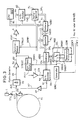
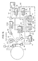
- FIG. 14 of a Sagnac interferometer with closed fiber loop shows a light source L, for example a laser, the parallel light beams of which are split into two light beams via a beam splitter ST1, are irradiated in the opposite direction into an interferometer fiber coil FS.
- the fiber spool FS will preferably consist of an optical single-mode fiber.
- the beam splitter ST1 also acts as a mixer for recombining the two light beams after passing through the fiber spool FS.
- the interference signal of the two superimposed light beams passes through the second beam splitter ST2 and its output branch AUS to a photodetector PD which scans the intensity of the interference image.
- the optical Power density at the input of the photodetector PD and the measurement sensitivity is referred to the literature mentioned.
- the sensitivity of the interferometer can be increased by applying a constant, non-reciprocal bias to the two opposing light beams in the fiber coil FS, in such a way that the two opposing light beams (light waves) periodically in the Working point of highest sensitivity of the interferometer can be shifted by an angle of (2n + 1) ⁇ / 2, where n is an integer.
- the phase modulator PM is initially excited with a signal ⁇ 1 (t), which causes a periodic phase shift of, for example, ⁇ ⁇ / 2, 3 / 2 ⁇ , ..., and whose period is 2t0, with t0 the duration of one Light wave in the fiber coil FS is called.
- phase ramp signal in which the amplitude of a sawtooth or the height of a step is equal to ⁇ , while the duration of a sawtooth or a step has the duration t0 or an integral multiple of corresponds to t0.
- the function of the circuit according to FIG. 14 is to generate a reciprocal, alternating phase shift in time with the frequency f0 which optimizes the operating point and the step-shaped ramp reset signal including a scale factor control is briefly described below:
- the demodulated output signal is fed via an amplifier A, which is generally combined with a filter, as signal VA to an analog / digital converter AD, the digital output signal of which is proportional to the rotation rate and contains sign information with regard to the direction of rotation.
- the signal VAD then arrives at a circuit GSC, which essentially contains and enters a digital integrator
- Composite phase control signal VSC delivers, as a composite signal consisting of the digital phase ramp reset signal and the digital phase modulation signal.
- the composite digital signal VSC is then converted into an analog control voltage VC in a digital / analog converter DA and applied as a control voltage to the phase modulator PM via a driver amplifier AP.
- the circuit GSC for generating the signal VSC comprises a first memory M1 for temporarily storing the digital signal VAD, the buffered output signals SM1 arrive at a first input e1 of an adder ADD, which is connected in cascade to a second memory M2.
- the output signals VSC buffered in the second memory M2 are fed back to a second input e2 of the adder ADD and added to the digital value of the rotation rate signal.
- the output signal SADD of the adder ADD thus corresponds to the angle of rotation.
- phase modulation signal and the phase ramp reset signal is synchronized and controlled by a central processor CPU via a bidirectional bus BC, which is connected to a quartz-stabilized oscillator OSC, which supplies the frequency f0.
- the latter supplies an overflow signal at an output SL via the bus BC to the central processor CPU.
- the central processor CPU generates the various control and synchronization signals, whereby to achieve a scale factor correction possible, depending on the overflow of the adder ADD, the modulation stroke is switched between a "mode A” and a "mode B", such that a modulation stroke of, for example, ⁇ ⁇ / 2 for mode A and a modulation stroke of ⁇ for mode B 3 / 2 ⁇ applies.
- the detected amplitude differences between the operating states with different modulation strokes are a measure of the scale factor error at the times of the phase ramp signal overflow.
- the known circuit according to FIG. 14 is equipped with a demodulator SFC which detects the amplitude differences of the f0 modulation signal in mode A (phase shift e.g. ⁇ ⁇ / 2) and mode B (phase shift e.g. ⁇ 3 / 2 ⁇ ) detected and this demodulated signal via an integrating amplifier IA as an analog correction signal SIA to a correcting analog input e M of the digital / analog converter DA.
- Switching from "Mode A” to “Mode B” is directly dependent on the ramp value of the resetting sawtooth signal and thus on the angle of rotation of the gyro.
- a ramp run can correspond to an angular increment of, for example, approximately four arc seconds.
- the modulation stroke switchover triggers the amplitude of the Modulation signal and effectively interspersing it in the sensitive signal path of the photodetector signal VD to switch the gyro bias.
- These undesirable stray effects are indicated in the circuit according to FIG. 14 by the dashed line and the coupling factor K.
- this switching of the modulation stroke signal is dependent on the angle of rotation, it leads to an insensitivity range (“lock-in") of the gyro. It can also be shown, as explained below, that this effect leads to a scale factor non-linearity outside the lock-in zone.
- This alternating frequency is proportional to the rotation rate, ie, according to the example explained in the cited US patent specification, a return of 2 ⁇ corresponds to an angular increment of 5 arc seconds; at 1 Hz return frequency, this corresponds to a rotation rate of 5 ° / h.
- EMC e lektro- m agnetic V tolerability; English: EMC measures, e lectro- m agnetic c ompatibility), ie want to eliminate or at least reduce by shielding (indicated in Fig. 14 by shielding the connecting line from the driver amplifier AP to the phase modulator PM) and the installation of filters in signal and voltage supply lines.
- shielding indicated in Fig. 14 by shielding the connecting line from the driver amplifier AP to the phase modulator PM
- the signal VSC or VC, VC 'contains the modulation frequency f0 1 / 2t0, which is generated in the oscillator OSC or via the processor CPU.
- the photodetector signal VD contains the rotation rate information with the same frequency and phase position. This signal is detected in the synchronous demodulator SYNCD.
- the circuit groups that generate the modulation size of the frequency f0 and the circuit parts that carry the rate-sensitive signal of the same frequency are closely related and usually have to be fed from a common power supply device.
- the risk of electromagnetic energy of frequency f0 being scattered into the sensitive signal path (signal VD) is thus obvious.
- Blocking filter for f0 in the Si Signal lines are not possible because the desired signal information is available at precisely this frequency. Undesired interferences can z. B. can only be reduced to a certain extent by shielding the amplifier Aul and the synchronous demodulator SYNCD against the rest of the circuit and by filtering its current supply.
- the spectral component with the frequency f0 in the signal VC or VC ′ is generally in the range of a few V.
- the rotation rate signal VD corresponds - depending on the light output, detector sensitivity and gyro scale factor - Voltages in the range of a few nV with a rotation rate of 1 ° / h.
- the closed-loop control loop is used to regulate the ramp slope of the reset signal in proportion to the sum of the true input rotation rate D e and the respective bias B a or B b , depending on whether modulation mode A or B is present.
- the slope during mode B is flatter than in mode A, since B b ⁇ B a is assumed.
- the duty cycle of the modes (T a / T b ) also depends on D e . From this follows the scale factor non-linearity mentioned above.
- the system switches to mode B.
- the control then triggers a negative ramp slope, since (D e + B b ) ⁇ 0 now applies, ie the ramp slope changes its sign and thus leaves the overflow area and mode A applies again.
- This mode A has a positive one again Ramp incline until switching back to mode B, etc.
- the control is therefore "trapped", ie the interferometer arrangement is in the lock-in state. How quickly the "zigzag ramp” shown in FIG. 2 changes between modes A and B at the overflow limit determines the speed of the control; this is generally very high.
- the lock-in state applies to an input rotation rate range in which the specified inequalities are fulfilled, ie the lock-in range has a width of
- the respective ramp value means the instantaneous value of the (unmodulated) ramp ⁇ (t).
- This ramp value is proportional to the angle of rotation and corresponds to the signal SADD.
- the ramp slope d ⁇ / dt corresponds to the time derivative of the angle of rotation, i.e. the rate of rotation.
- the problem with the known ramp reset method is that the ramp value, ie the value of the angle of rotation, is the criterion for whether operating mode A or B and thus the different biases B a or B b are present and because of B a ⁇ B b influence the ramp slope itself.
- the scale factor error information is, as shown, in the form of an intensity change signal, the frequency of which is proportional to the rotation rate and can change between 0 and approximately 100 kHz if the theoretical duty cycle of the modulation strokes between mode A and mode B is 1: 3.
- the apparent advantage that the information-bearing intensity changes occur more frequently at high rotation rates and thus better scale factor error information is available at high rotation rates is, however, opposed by the fact that the associated signal processing device has to process a comparatively high frequency range.
- the known ramp reset method leads to the absence of the scale factor error information in the region of the rotation rate zero and thus to drift problems.
- the invention is therefore based on the object, the insensitivity range of a fiber optic rotation rate sensor to avoid at low rotation rates, ie the "lock-in effect" shown, and to obtain easily processed signals for regulating the scale factor.
- the automatic rotation angle-dependent modulation stroke change in the ramp overflow was the main cause of the lock-in effect of the known method, the scale factor non-linearity and the wide rotation rate-dependent Frequency range of the scale factor error information is.
- the invention is thus aimed at the goal of developing a modulation method for the ramp reset method which, on the one hand, includes the modulation stroke switchover from mode A to mode B for obtaining the scale factor error information, but on the other hand this switchover in a specific, e.g. B. fixed clock and no longer dependent on the angle of rotation.
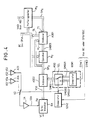
- the invention consists in a fiber optic Sagnac interferometer for measuring the rotation rate of the type mentioned at the beginning, as indicated in the preamble of claim 1, that between the digital integrator and the digital / analog converter, a (second) digital adder is arranged, which is acted upon at a second input with the modulation stroke signal which can be switched between the two operating modes in a predetermined cycle from a first pulse generator clocked with the frequency f0, which for the first operating mode A has a signal corresponding to the phase shift ⁇ ⁇ / 4 and for the second Operating mode B outputs a signal corresponding to the phase shift ⁇ 3 / 4 ⁇ to the second input of the (second) digital adder.
- the signal VSY1 corresponding to a control deviation of the rotation rate control loop is amplified in the amplifier A and delivers the signal VA.
- the amplifier A also contains a filter that determines the control properties of the entire control circuit and is dimensioned according to known design methods of control technology; in this regard, reference is made to the document US-A-4 705 399, which has already been mentioned several times.
- the output signal VA will have a portion of the time integral of the input signal VSY1.
- the signal VA is digitized in the analog / digital converter AD and the resulting digital signal VAD is stored in the memory M1, these processes being controlled by the processor CPU via the bus BC.
- the output signal SM1 acts on the input e 1 of the adder, which is referred to here as the first adder ADD1 for better differentiation of a further adder.
- the output signal SADD1 of the first adder ADD1 is fed to the memory M2, the output signal SM2 of which is fed to the further input e2 of the first adder ADD1, entirely in accordance with the known circuit according to FIG. 14.
- the first adder ADD1 together with the memory M2 and the associated control Via the bus BC represents a ramp signal generator which generates a ramp or step signal SM2, the step height of which corresponds to the value SM1 and the step width of which corresponds to the light propagation time t0.
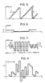
- a ramp overflow of the signal SM2 is achieved when a certain output value of the first adder ADD1 is exceeded, which is shown schematically in FIG. 5.
- the overflow properties of digital binary number codes can advantageously be used.
- This signal referred to as the second signal component SM2
- the second signal component SM2 is - in contrast to the known circuit according to FIG. 14 - supplied to the optical phase modulator PM via electronic modules to be described and causes a phase shift ⁇ R , which is limited to a phase range of essentially 2 ⁇ by the overflow mentioned (cf. FIG. 5).
- a substantially rectangular modulation signal SMOD is added to the signal SM2 in a second adder ADD2, from which the composite modulation signal VSC arises.
- the modulation signal SMOD is generated in a modulation signal generator MOD and has the gyro frequency f0.
- the modulation signal generator MOD is synchronized by the processor CPU or by the oscillator OSC via a signal SYNC1. Via a signal SMODS (see FIG. 6), which is taken from the already mentioned second pulse generator GEN2, the amplitude of the signal SMOD can be changed by a factor of 3 in a manner which will be explained in more detail below.
- the signal component SMOD (cf. FIG.
- This signal component SMOD causes a phase shift ⁇ M which is essentially ⁇ ⁇ / 4 or ⁇ 3 / 4 ⁇ (see FIG. 7).
- the amplitude of the modulation ⁇ M is therefore controlled by the signal SMODS.
- the state, during which the amplitude is ⁇ ⁇ / 4, is, as already explained above, “mode A”, while “mode B” is set for the larger modulation amplitude deviation of ⁇ 3 / 4 ⁇ .
- the modulation amplitude switchover can be carried out, for example, in such a way that two signals SMOD1 corresponding to the explained mode A and SMOD2 corresponding to the mode B with the explained amplitudes are generated in a generator GEN1 and alternately via a selector controlled by the signal SMODS SEL as Signal SMOD act on the second input of the second adder ADD2.
- the digital processing word width of the second adder ADD2 is designed such that the output signal VSC always corresponds to the sum of the input signals SM2 or SMOD without the result overflowing.
- the combined signal VSC (see FIG. 8) is supplied to the digital / analog converter DA in the manner already explained and converted into the voltage signal VC and amplified to the signal VC ', the value of which is essentially proportional to the numerical value of the signal VSC.
- the voltage VC ' causes a phase shift ⁇ C in the optical phase modulator PM (see again FIG. 8).
- the circuit modified according to FIG. 3 is based on the following principle:
- the unmodulated digital ramp value is limited to the phase angle range 2 ⁇ or ⁇ ⁇ by cutting off above the bit of the value ⁇ .
- this limited ramp is added a square wave signal generated in the first pulse generator GEN1, SEL or MOD, which has the modulation frequency f0, but in the amplitude corresponding to a phase angle value of ⁇ ⁇ / 4 (mode A) and ⁇ 3 / 4 ⁇ (Mode B) is switchable.
- This changeover is controlled by the second pulse generator GEN2, the frequency and duty cycle of which can be freely selected.
- the switchover values can be predefined by the processor CPU or can be controlled depending on the rotation rate, whereby synchronization with the modulation frequency f0 makes sense.
- the modulated ramp signal shown in FIG. 8, which is fed to the phase modulator PM, gives rise to an intensity signal I (t) at its output via the interferometer, which essentially satisfies the following relationship: I (t) ⁇ cos ( ⁇ (t) + ⁇ 0 (t)) where ⁇ (t) ⁇ c (t) - ⁇ c (t-t0) applies; ⁇ c (t) is the phase shift at the phase modulator PM and ⁇ 0 (t) is the rotation rate proportional Sagnac phase shift caused by given is.
- the length l and D the mean diameter of the light path in the fiber coil FS, ⁇ the wavelength of the light used, c the vacuum speed of light and ⁇ the rotation rate.
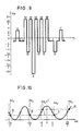
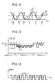
- the signal ⁇ (t) is shown in Fig. 9. 10 shows the resulting intensity curve as a function of ⁇ (t) and ⁇ 0 (t). As can be seen from these two figures, the angular rate-proportional phase shift ⁇ 0 (t) leads to an increase in the intensity I in the time periods "I” and “IV” and in the time periods “II", “III” and “V” sinks.
- the resulting temporal intensity curve I (t) is shown in FIG. 12.
- the intensity difference ⁇ I0 is detected with the aid of the first synchronous demodulator SYNCD1 and is used to regulate the ramp gradient of the signal ⁇ R (cf. FIG. 5), with which the effect of ⁇ 0 by the mean value of the phase shift ⁇ , the same amount, but has a different sign, is compensated.
- the following then applies to the intensity I (t): I (t) ⁇ cos ( ⁇ (t) + ⁇ 0 (t)) const.
- the mentioned angle increment value ⁇ is approximately 4 angular seconds.
- This overflow information can be given, for example, by the first adder ADD1 via its overflow output signal SL and the bus BC to the processor CPU, which counts (adds up) the angular increments.
- the output signal VSY2 of the second synchronous demodulator SYNCD2 is a measure of the scale factor error.
- This error signal acts on the integrating amplifier IA, which represents a filter that is dimensioned according to control engineering aspects and determines the control engineering properties of the scale factor control.
- the output signal SIA contains at least a portion that corresponds to the time integral of the input signal VSY2.
- the signal SIA is fed to the input e M of the digital / analog converter DA.
- the digital / analog converter DA can be referred to as a multiplying digital / analog converter, ie its output variable VC is essentially proportional to the product of the two signals VSC (digital) and SIA (analog).
- the voltage swing of the signal VC is regulated in such a way that the modulation phase swing at the opti phase modulator PM is exactly ⁇ ⁇ / 4 (mode A) or ⁇ 3 / 4 ⁇ (mode B). This also ensures that the overflow-related return of phase ⁇ R (cf. FIG. 5) corresponds exactly to 2 ⁇ .
- Fig. 11 it is shown how with existing scale factor errors - here, for example, the type that the optical phase shift is smaller than desired - the intensity course-determining working points I, II, III, IV or V to the working points I ', II', III ', IV', V 'move and thus the aforementioned change in intensity ⁇ I1 (Fig. 12) arises.
- the output amplitude of the signal VC and thus the optical phase shift is increased so that the desired operating points I, II, III, IV, V are reached again and the Intensity change ⁇ I1 becomes zero.
- FIG. 13 also shows the synchronization signal DEMR1 to be supplied to the first synchronous demodulator SYND1 via the bus BC.
- the (partial) circuit shown in FIG. 4 corresponds in its mode of operation to that of FIG. 3 completely.
- the only difference is the second synchronous demodulator, which here - analogous to FIG. 14 of the document US-A-4 705 399 - is formed by two differential amplifiers A14 and A23, which are represented in a manner not shown at their plus or minus inputs by the Signals VS1, VS2 and VS4, VS3 are acted upon by four sample and hold circuits.
- the output-side changeover switch K2 via which the intensity change signal ultimately acts on the integrating amplifier IA, is controlled by the freely selectable but fixed output signal SMODS of the second pulse generator GEN2, that is to say in time with the predetermined mode or modulation stroke switchover.
- a scattering of the different modulation stroke still causes a change in bias.
- this is no longer dependent on the yaw rate, rather its value is constant and corresponds to the duty-weighted average of the bias values of both modulation strokes. Since the frequency and the pulse duty factor with which the modulation stroke change is controlled and with which the scale error information is obtained are freely selectable and, above all, known, the scale factor control can be optimized to a fixed frequency.
- the invention offers the decisive advantage that the lock-in effect described and the associated scale factor non-linearity are avoided and signals for scale factor control that are more economical to process are available.
- the additional circuitry required in the digital part of the control electronics is comparatively low and is not significant when using modern integrated circuits.
- the central processor can and will generally be implemented by a commercially available microprocessor. It is also possible to implement "hard-wired" logic without deviating from the inventive concept.
Abstract
Description
Die Erfindung betrifft ein faseroptisches Sagnac-Interferometer zur Drehratenmessung, bei dem zwei aus einer Lichtquelle stammende, durch Strahlteilung erzeugte Lichtstrahlen in entgegengesetzten Richtungen in eine Faserspule eingestrahlt und anschließend wiedervereinigt werden, bei dem das entstehende Interferenzbild durch eine Detektoreinrichtung abgetastet wird, deren Ausgangssignal der Lichtintensität des Interferenzbildes entspricht, bei dem die beiden Lichtstrahlen mittels eines in der Faserspule liegenden Phasenmodulators durch ein periodisches, aus mehreren variablen Signalanteilen zusammengesetztes Rechtecksignal mit der Grundfrequenz f₀ = ¹/2t₀, wobei t₀ der Laufzeit jedes der Lichtstrahlen durch die Faserspule entspricht, moduliert werden, und wobei ein erster Signalanteil bei periodischem Modulationshubwechsel zwischen zwei Betriebsmodi im Takt der Frequenz f₀ eine reziproke alternierende Phasenverschiebung der beiden gegenläufigen Lichtstrahlen be wirkt und wobei weiter ein zweiter Signalanteil ein stufenförmiges Rampensignal ist, dessen Stufen jeweils eine der Laufzeit t₀ bzw. ganzzahligen Vielfachen von t₀ entsprechende Dauer und Amplitudeninkremente aufweisen, welche nicht-reziproke inkrementale Phasenverschiebungen der beiden Lichtstrahlen kompensieren, bei dem das verstärkte Photodetektorausgangssignal einem mit der Frequenz f₀ getakteten ersten Synchrondemodulator zugeführt wird, bei dem das demodulierte und verstärkte Ausgangssignal einem Analog/Digital-Wandler zugeführt und nach Digitalisierung in einen digitalen Integrator integriert und mit nicht-reziproken Phasenverschiebungen der Lichtstrahlen über den zweiten Signalanteil kompensierender Phase über einen Digital/Analog-Wandler und einen Treiberverstärker den Phasenmodulator beaufschlagt, bei dem eine Skalenfaktorkorrekturschaltung vorgesehen ist, die das verstärkte Photodetektor-Ausgangssignal im Takt der Modusumschaltung demoduliert und über einen integrierenden Verstärker ein analoges Skalenfaktor-Korrektursignal an den Digital/Analog-Wandler abgibt und bei dem ein vom Quarzoszillator getakteter Prozessor die Steuer- und Synchronisationssignale für den ersten Synchrondemodulator, den Analog/Digital-Wandler und den digitalen Integrator liefert.The invention relates to a fiber optic Sagnac interferometer for measuring the rate of rotation, in which two light beams originating from a light source and generated by beam splitting are irradiated in opposite directions into a fiber coil and then reunited, in which the resulting interference image is scanned by a detector device, the output signal of the light intensity corresponds to the interference pattern, in which the two light beams are modulated by means of a phase modulator located in the fiber coil by a periodic square wave signal composed of several variable signal components with the fundamental frequency f₀ = ½ t, where t₀ corresponds to the transit time of each of the light beams through the fiber coil, and wherein a first signal component in the case of a periodic change of modulation stroke between two operating modes in time with the frequency f₀ is a reciprocal alternating phase shift of the two opposite light beams acts and further a second signal component is a step-shaped ramp signal, the steps of which each have a duration and amplitude increments corresponding to the transit time t₀ or integer multiples of t₀, which compensate for non-reciprocal incremental phase shifts of the two light beams, in which the amplified photodetector output signal matches one with the Frequency f₀ clocked first synchronous demodulator is supplied, in which the demodulated and amplified output signal is supplied to an analog / digital converter and after digitization integrated in a digital integrator and with non-reciprocal phase shifts of the light beams over the second signal component compensating phase via a digital / analog Converter and a driver amplifier applied to the phase modulator, in which a scale factor correction circuit is provided, which demodulates the amplified photodetector output signal in time with the mode switchover and via an i integrating amplifier delivers an analog scale factor correction signal to the digital / analog converter and in which a processor clocked by the crystal oscillator supplies the control and synchronization signals for the first synchronous demodulator, the analog / digital converter and the digital integrator.
Zum Messen nichtreziproker Phasenverschiebungen in einem faseroptischen Sagnac-Interferometer, auch Ringinterferometer genannt, ist es aus der Druckschrift DE-Al-31 44 162 bekannt, im Bereich eines Eingangs der Faserspule liegenden Phasenmodulator einerseits mit einem mit der Frequenz f₀ = ¹/2t₀ umschaltbaren Phasenhub bestimmter Amplitude und andererseits mit einer den Phasenhub ebenfalls verschiebenden Sägezahnspannung zur Nachregelung der nichtreziproken Phasenverschiebungen, z. B. aufgrund von Drehraten, zu beaufschlagen, wobei mit t₀ die Laufzeit jedes der Lichtstrahlen durch die Faserspule bezeichnet ist. Die Steigung der kompensierenden oder rückstellenden Sägezahnspannung (Phasen rampe) entspricht der Drehrate, ist also proportional zu Δφ₀/t₀, wobei mit φ₀ die nichtreziproke Phasenverschiebung, beispielsweise verursacht durch eine Drehbewegung, bezeichnet ist. In der Praxis jedoch ist das in der genannten DE-Druckschrift beschriebene, sogenannte Phasenrampen-Rückstellverfahren kaum brauchbar, weil für inertiale Drehratenmessungen Genauigkeiten, insbesondere hinsichtlich der umschaltbaren Phasenhübe, der Amplitude bzw. Steigung des Rückstellsignals sowie des Proportionalitäts- oder Skalenfaktors verlangt werden, die sich in analoger Schaltungstechnik nicht gewährleisten lassen.For measuring non-reciprocal phase shifts in a fiber-optic Sagnac interferometer, also called ring interferometer, it is known from the document DE-Al-31 44 162, in the area of an input of the fiber coil, on the one hand, with a phase shift which can be switched over with the frequency f₀ = ½ t certain amplitude and on the other hand with a sawtooth voltage also shifting the phase shift for readjustment of the non-reciprocal phase shifts, e.g. B. due to yaw rates, with t₀ the transit time of each of the light rays through the fiber spool is designated. The slope of the compensating or restoring sawtooth voltage (phases ramp) corresponds to the yaw rate, is therefore proportional to Δφ₀ / t₀, where φ₀ denotes the non-reciprocal phase shift, for example caused by a rotational movement. In practice, however, the so-called phase ramp reset method described in the above-mentioned DE publication is hardly usable because accuracies are required for inertial rotation rate measurements, in particular with regard to the switchable phase shifts, the amplitude or slope of the reset signal and the proportionality or scale factor, which are required cannot be guaranteed in analog circuit technology.
Mit der US-A-4 705 399 (=̂ EP-A1-0 168 292) ist eine bemerkenswerte Weiterentwicklung des in der genannten DE-Druckschrift grundsätzlich beschriebenen Rampenrückstellverfahrens für faseroptische Ringinterferometer bekannt geworden, das hinsichtlich der Signalauswertung und -aufbereitung vollständig digital arbeitet, so daß sich die erforderliche Signalpräzision insbesondere hinsichtlich der Genauigkeit der umschaltbaren Phasenhübe und des Rampen-Rückstellsignals mit eindeutiger Zuordnung einer automatischen Meßbereichumschaltung sowie einer Korrektur der Skalenfaktoren gewinnen lassen. Anhand der Fig. 14, die - in vereinfachter Darstellung - dem Stand der Technik nach Fig. 14 der genannten Druckschrift US-A-4 705 399 entspricht (vgl. auch H.C. Lefevre et al. in Integrated Optics: "A practical solution for the Fiber-Optic Gyroscope", SPIE Vol. 719, Fiber Optic Gyros, 1986), wird zunächst das Funktionsprinzip des digitalen Phasenrampenrückstellverfahrens für faseroptische Drehratensensoren nach dem Stand der Technik erläutert, wobei hinsichtlich der Einzelheiten auf die genannte Literatur verwiesen wird:US-A-4 705 399 (= ̂ EP-A1-0 168 292) has made a remarkable further development of the ramp reset method for fiber-optic ring interferometers, which is described in principle in the above-mentioned DE publication, and which works completely digitally with regard to signal evaluation and processing , so that the required signal precision can be obtained in particular with regard to the accuracy of the switchable phase shifts and the ramp reset signal with a clear assignment of an automatic measuring range switchover and a correction of the scale factors. 14, which - in a simplified representation - corresponds to the prior art according to FIG. 14 of the cited document US-A-4 705 399 (cf. also HC Lefevre et al. In Integrated Optics: "A practical solution for the Fiber-Optic Gyroscope ", SPIE Vol. 719, Fiber Optic Gyros, 1986), the functional principle of the digital phase ramp reset method for fiber-optic rotation rate sensors according to the prior art is first explained, reference being made to the cited literature for details:
Die schematische Darstellung der Fig. 14 eines dem genannten Stand der Technik entsprechenden Sagnac-Interferometers mit geschlossener Faserschleife zeigt eine Lichtquelle L, beispielsweise einen Laser, dessen parallele Lichtstrahlen, über einen Strahlteiler ST1 in zwei Lichtstrahlen aufteilt, in entgegengesetzter Richtung in eine Interferometer-Faserspule FS eingestrahlt werden. Die Faserspule FS wird vorzugsweise aus einer optischen Monomodefaser bestehen. Der Strahlteiler ST1 wirkt gleichzeitig als Mischer zur Rekombination der beiden Lichtstrahlen nach Durchlaufen der Faserspule FS. Das Interferenzsignal der beiden überlagerten Lichtrahlen gelangt über den zweiten Strahlteiler ST2 und dessen Ausgangszweig AUS auf einen Photodetektor PD, der die Intensität des Interferenzbildes abtastet. Wird mit Δφ₀ die Phasendifferenz zwischen den beiden sich in entgegengesetzten Richtungen in der geschlossenen Faserspule FS ausbreitenden Lichtstrahlen bezeichnet, so gilt, solange keine nichtreziproken Störungen vorliegen: Δφ₀ = 0. Hinsichtlich des mathematischen Zusammenhangs zwischen der Phasendifferenz Δφ₀ und der Drehrate oder Drehgeschwindigkeit, der optischen Leistungsdichte am Eingang des Photodetektors PD und der Meßempfindlichkeit wird auf die genannte Literatur verwiesen. Dort ist auch beschrieben, wie die Empfindlichkeit des Interferometers durch Beaufschlagung der beiden gegenläufigen Lichtstrahlen in der Faserspule FS durch Einführung eines konstanten, nichtreziproken Bias erhöht werden kann, und zwar so, daß mittels eines Phasenmodulators PM die beiden gegenläufigen Lichtstrahlen (Lichtwellen) periodisch in den Arbeitspunkt höchster Empfindlichkeit des Interferometers um Winkel von (2n + 1) π/2 verschoben werden, wobei n eine ganze Zahl ist. Zu diesem Zweck wird der Phasenmodulator PM also zunächst mit einem Signal φ₁(t) erregt, das eine periodische Phasenverschiebung von beispielsweise ± π/2, 3/2π , ..., bewirkt und dessen Periode 2t₀ beträgt, wobei mit t₀ die Laufzeit einer Lichtwelle in der Faserspule FS bezeichnet ist.The schematic representation of FIG. 14 of a Sagnac interferometer with closed fiber loop corresponding to the prior art mentioned shows a light source L, for example a laser, the parallel light beams of which are split into two light beams via a beam splitter ST1, are irradiated in the opposite direction into an interferometer fiber coil FS. The fiber spool FS will preferably consist of an optical single-mode fiber. The beam splitter ST1 also acts as a mixer for recombining the two light beams after passing through the fiber spool FS. The interference signal of the two superimposed light beams passes through the second beam splitter ST2 and its output branch AUS to a photodetector PD which scans the intensity of the interference image. If the phase difference between the two light beams propagating in opposite directions in the closed fiber coil FS is designated with Δφ₀, as long as there are no non-reciprocal disturbances: Δφ₀ = 0. With regard to the mathematical relationship between the phase difference Δφ₀ and the rotation rate or rotational speed, the optical Power density at the input of the photodetector PD and the measurement sensitivity is referred to the literature mentioned. There it is also described how the sensitivity of the interferometer can be increased by applying a constant, non-reciprocal bias to the two opposing light beams in the fiber coil FS, in such a way that the two opposing light beams (light waves) periodically in the Working point of highest sensitivity of the interferometer can be shifted by an angle of (2n + 1) π / 2, where n is an integer. For this purpose, the phase modulator PM is initially excited with a signal φ₁ (t), which causes a periodic phase shift of, for example, ± π / 2, 3 / 2π, ..., and whose period is 2t₀, with t₀ the duration of one Light wave in the fiber coil FS is called.
Bei der Schaltung nach Fig. 14 werden, wie in der genannten US-Patentschrift beschrieben, nichtreziproke Phasenver schiebungen durch eine negative Rückkopplung auf den Phasenmodulator PM kompensiert durch ein sogenanntes Phasenrampensignal, dessen Steigung proportional ist zu Δφ/₀ , d. h. zu Δφ, also der nichtreziproke Phasenverschiebung. Das rückstellende Phasenrampensignal ist bei der Schaltung nach Fig. 14 ein Sägezahn- oder Treppenstufensignal, bei dem die Amplitude eines Sägezahns bzw. die Höhe einer Treppenstufe gleich Δφ beträgt, während die Dauer eines Sägezahns oder einer Treppenstufe der Laufzeit t₀ bzw. einem ganzzahligen Vielfachen von t₀ entspricht.In the circuit of FIG. 14, as described in the aforementioned US patent, non-reciprocal phase ver shifts due to a negative feedback on the phase modulator PM compensated by a so-called phase ramp signal, the slope of which is proportional to Δφ / ₀, ie to Δφ, ie the non-reciprocal phase shift. The resetting phase ramp signal in the circuit according to FIG. 14 is a sawtooth or step signal, in which the amplitude of a sawtooth or the height of a step is equal to Δφ, while the duration of a sawtooth or a step has the duration t₀ or an integral multiple of corresponds to t₀.
Dieses in der Literatur, insbesondere der genannten US-A-4 705 399 beschriebene digitale Phasenrampenprinzip hat gegenüber einer analogen Lösung den entscheidenden Vorteil, daß die Skalenfaktoren des Phasenmodulationssteuersignals und des Phasenrampenrückstellsignals wenigstens im Prinzip korrigiert sind und eine präzise Definition der Sägezahnamplituden des Rückstellsignals gewährleistet ist.This digital phase ramp principle described in the literature, in particular the aforementioned US-A-4 705 399, has the decisive advantage over an analog solution that the scale factors of the phase modulation control signal and the phase ramp reset signal are corrected at least in principle and a precise definition of the sawtooth amplitudes of the reset signal is ensured .
Die Funktion der Schaltung nach Fig. 14 ist zur Erzeugung einer den Arbeitspunkt optimierenden reziproken, alternierenden Phasenverschiebung im Takt der Frequenz f₀ sowie des stufenförmigen Rampenrückstellsignals einschließlich einer Skalenfaktorregelung wird nachfolgend kurz beschrieben:The function of the circuit according to FIG. 14 is to generate a reciprocal, alternating phase shift in time with the frequency f₀ which optimizes the operating point and the step-shaped ramp reset signal including a scale factor control is briefly described below:
Das Ausgangssignal VD des Photodetektors PD wird über einen Impedanzwandler und Verstärker A₀ angehoben, dessen Ausgangssignal VD′ einen Synchrondemodulator SYNCD speist, der auf die Abtastfrequenz f₀ = ¹/2t₀ synchronisiert ist. Das demodulierte Ausgangssignal gelangt über einen in der Regel mit einem Filter kombinierten Verstärker A als Signal VA auf einen Analog/Digital-Wandler AD, dessen digitales Ausgangssignal proportional ist zur Drehrate und eine Vorzeicheninformation hinsichtlich der Drehrichtung enthält. Das Signal VAD gelangt sodann auf eine Schaltung GSC, die im wesentlichen einen digitalen Integrator beinhaltet und ein zusammengesetztes Phasensteuersignal VSC liefert, als zusammengesetztes Signal bestehend aus dem digitalen Phasenrampen-Rückstellsignal und dem digitalen Phasenmodulationssignal. Das zusammengesetzte Digitalsignal VSC wird anschließend in einem Digital/Analog-Wandler DA in eine analoge Steuerspannung VC gewandelt und über einen Treiberverstärker AP als Steuerspannung auf den Phasenmodulator PM gegeben.The output signal VD of the photodetector PD is raised via an impedance converter and amplifier A₀, whose output signal VD 'feeds a synchronous demodulator SYNCD, which is synchronized to the sampling frequency f₀ = ½ / 2t₀. The demodulated output signal is fed via an amplifier A, which is generally combined with a filter, as signal VA to an analog / digital converter AD, the digital output signal of which is proportional to the rotation rate and contains sign information with regard to the direction of rotation. The signal VAD then arrives at a circuit GSC, which essentially contains and enters a digital integrator Composite phase control signal VSC delivers, as a composite signal consisting of the digital phase ramp reset signal and the digital phase modulation signal. The composite digital signal VSC is then converted into an analog control voltage VC in a digital / analog converter DA and applied as a control voltage to the phase modulator PM via a driver amplifier AP.
Die Schaltung GSC zur Erzeugung des Signals VSC umfaßt einen ersten Speicher M₁ zur Zwischenspeicherung des Digitalsignals VAD, dessen zwischengespeicherte Ausgangssignale SM₁ auf einen ersten Eingang e₁ eines Addierers ADD gelangen, der in Kaskade mit einem zweiten Speicher M₂ verbunden ist. Die im zweiten Speicher M₂ zwischengespeicherten Ausgangssignale VSC werden auf einen zweiten Eingang e₂ des Addierers ADD rückgeführt und zum Digitalwert des Drehratensignals hinzuaddiert. Das Ausgangssignal SADD des Addierers ADD entspricht damit dem Drehwinkel.The circuit GSC for generating the signal VSC comprises a first memory M₁ for temporarily storing the digital signal VAD, the buffered output signals SM₁ arrive at a first input e₁ of an adder ADD, which is connected in cascade to a second memory M₂. The output signals VSC buffered in the second memory M₂ are fed back to a second input e₂ of the adder ADD and added to the digital value of the rotation rate signal. The output signal SADD of the adder ADD thus corresponds to the angle of rotation.
Die soweit beschriebene Schaltung zur Erzeugung des Phasenmodulationssignals und des Phasenrampen-Rückstellsignals wird von einem Zentralprozessor CPU über einen bidirektionalen Bus BC synchronisiert und gesteuert, der mit einem quarzstabilisierten Oszillator OSC verbunden ist, der die Frequenz f₀ liefert.The circuit described so far for generating the phase modulation signal and the phase ramp reset signal is synchronized and controlled by a central processor CPU via a bidirectional bus BC, which is connected to a quartz-stabilized oscillator OSC, which supplies the frequency f₀.
Abgesehen von der auf einen bestimmten Drehwinkel, z. B. vier Bogensekunden, bezogenen Anzahl von Bits pro Wort, die der Kapazität des Addierers ADD entsprechen, liefert letzterer ein Überlaufsignal an einem Ausgang SL über den Bus BC an den Zentralprozessor CPU. In Abhängigkeit von den Überlaufsignalen des Addierers und in Übereinstimmung mit dem Taktsignal des Oszillators OSC generiert der Zentralprozessor CPU die verschiedenen Steuer- und Synchronisationssignale, wobei, um eine Skalenfaktorkorrektur zu er möglichen, in Abhängigkeit vom Überlauf des Addierers ADD der Modulationshub zwischen einem "Modus A" und einem "Modus B" umgeschaltet wird, derart, daß für den Modus A ein Modulationshub von beispielsweise ± π/2 und für den Modus B ein Modulationshub von ± 3/2π gilt. Wie in der genannten Literatur beschrieben, sind die detektierten Amplitudendifferenzen zwischen den Betriebszuständen mit unterschiedlichen Modulationshüben ein Maß für den Skalenfaktorfehler zu den Zeitpunkten des Phasenrampensignalüberlaufs. Um diesen Skalenfaktorfehler zu korrigieren, ist die bekannte Schaltung nach Fig. 14 mit einem Demodulator SFC ausgestattet, der die Amplitudenunterschiede des f₀-Modulationssignals im Modus A (Phasenhub z. B. ± π/2) und Modus B (Phasenhub z. B. ± 3/2π ) erfaßt und dieses demodulierte Signal über einen integrierenden Verstärker IA als analoges Korrektursignal SIA auf einen korrigierenden Analogeingang eM des Digital/Analog-Wandlers DA gibt.Apart from the on a certain angle of rotation, for. B. four arc seconds, related number of bits per word, which correspond to the capacity of the adder ADD, the latter supplies an overflow signal at an output SL via the bus BC to the central processor CPU. Depending on the overflow signals of the adder and in accordance with the clock signal of the oscillator OSC, the central processor CPU generates the various control and synchronization signals, whereby to achieve a scale factor correction possible, depending on the overflow of the adder ADD, the modulation stroke is switched between a "mode A" and a "mode B", such that a modulation stroke of, for example, ± π / 2 for mode A and a modulation stroke of ± for mode B 3 / 2π applies. As described in the literature mentioned, the detected amplitude differences between the operating states with different modulation strokes are a measure of the scale factor error at the times of the phase ramp signal overflow. In order to correct this scale factor error, the known circuit according to FIG. 14 is equipped with a demodulator SFC which detects the amplitude differences of the f₀ modulation signal in mode A (phase shift e.g. ± π / 2) and mode B (phase shift e.g. ± 3 / 2π) detected and this demodulated signal via an integrating amplifier IA as an analog correction signal SIA to a correcting analog input e M of the digital / analog converter DA.
Dieses soweit anhand der Fig. 14 kurz beschriebene Funktionsprinzip des digitalen Phasenrampen-Rückstellverfahrens für faseroptische Drehratensensoren, bei dem die Steigung der Phasenrampe ein Maß für die rückgestellte Drehrate ist und bei dem in der Rücksprungphase zur Gewinnung eines Korrektursignals für den Skalenfaktor eine Umschaltung des Modulationshubs im Verhältnis 1:3 erfolgt, führt in der Praxis des Betriebs von solchen inertialen Drehratenmeßeinrichtungen zu erheblichen Schwierigkeiten aus folgenden Gründen:This operating principle of the digital phase ramp reset method for fiber-optic rotation rate sensors, described briefly with reference to FIG. 14, in which the slope of the phase ramp is a measure of the reset rotation rate and in which in the return phase to obtain a correction signal for the scale factor, a switching of the modulation stroke in Ratio 1: 3 occurs, leads in practice to the operation of such inertial rotation rate measuring devices to considerable difficulties for the following reasons:
Die Umschaltung von "Modus A" auf "Modus B" ist direkt abhängig vom Rampenwert des rückstellenden Sägezahnsignals und damit vom Drehwinkel des Kreisels. Ein Rampendurchlauf kann dabei einem Winkelinkrement von beispielsweise ca. vier Bogensekunden entsprechen. Die Modulationshubumschaltung bewirkt aber über die Verdreifachung der Amplitude des Modulationssignals und über Einstreuungen desselben in den empfindlichen Signalpfad des Photodetektorsignals VD effektiv eine Umschaltung des Kreiselbias. Diese unerwünschten Einstreueffekte sind in der Schaltung nach Fig. 14 durch gestrichelte Linie und den Kopplungsfaktor K angedeutet. Da diese Umschaltung des Modulationshubsignals aber drehwinkelabhängig ist, führt sie zu einem Unempfindlichkeitsbereich ("lock-in") des Kreisels. Es läßt sich auch, wie nachfolgend erläutert, zeigen, daß dieser Effekt außerhalb der Lock-in-Zone zu einer Skalenfaktor-Nichtlinearität führt.Switching from "Mode A" to "Mode B" is directly dependent on the ramp value of the resetting sawtooth signal and thus on the angle of rotation of the gyro. A ramp run can correspond to an angular increment of, for example, approximately four arc seconds. However, the modulation stroke switchover triggers the amplitude of the Modulation signal and effectively interspersing it in the sensitive signal path of the photodetector signal VD to switch the gyro bias. These undesirable stray effects are indicated in the circuit according to FIG. 14 by the dashed line and the coupling factor K. However, since this switching of the modulation stroke signal is dependent on the angle of rotation, it leads to an insensitivity range ("lock-in") of the gyro. It can also be shown, as explained below, that this effect leads to a scale factor non-linearity outside the lock-in zone.
Wie in Fig. 13 der Druckschrift US-A-4 705 399 gezeigt, ergibt sich bei Vorliegen eines Skalenfaktorfehlers eine unterschiedliche mittlere Intensität I des Photodetektorsignals VD bei Modulationshüben des Modus A bzw. den Modulationshüben des Modus B. Diese Intensitätsdifferenz wird im integrierenden Verstärker IA aufintegriert und liefert das analoge Korrektursignal am Eingang eM des Digital/Analog-Wandlers DA. Die Intensitätswechselfrequenz ist gleich der Wechselfrequenz von Modus A auf Modus B und somit gleich der Rampensignal-Rücksprungfrequenz, da die Umschaltung z. B. von Modus A auf Modus B durch Rampenüberlauf, d. h. das Signal SL des Addierers ADD, entsteht. Diese Wechselfrequenz ist drehratenproportional, d. h. gemäß dem in der genannten US-Patentschrift erläuterten Beispiel entspricht ein Rücksprung von 2π einem Winkelinkrement von 5 Bogensekunden; bei 1 Hz Rücksprungfrequenz entspricht dies einer Drehrate von 5°/h.As shown in Fig. 13 of the document US-A-4 705 399, there is a different mean intensity I of the photodetector signal VD with modulation strokes of mode A or the modulation strokes of mode B when a scale factor error is present. This intensity difference is in the integrating amplifier IA integrates and supplies the analog correction signal at input e M of the digital / analog converter DA. The intensity change frequency is equal to the change frequency from mode A to mode B and thus equal to the ramp signal return frequency, since the switch z. B. from mode A to mode B by ramp overflow, ie the signal SL of the adder ADD, arises. This alternating frequency is proportional to the rotation rate, ie, according to the example explained in the cited US patent specification, a return of 2π corresponds to an angular increment of 5 arc seconds; at 1 Hz return frequency, this corresponds to a rotation rate of 5 ° / h.
Bei kleinen Drehraten kann diese Wechselfrequenz beliebig klein werden, weshalb der integrierende Verstärker IA nur selten die Intensitätsunterschiedinformation erhält. In den dann beliebig langen Intervallen, in denen der Modus nicht wechselt, fehlt dem integrierenden Verstärker IA diese Information, und jeder kleine elektrische Nullpunktfehler an seinem Eingang läßt seine Ausgangsgröße, also das Skalen faktorkorrektursignal SIA weglaufen (driften). Aus diesem Grund ist der Skalenfaktor bei niedrigen Drehraten anfällig gegen Driften des integrierenden Verstärkers IA. Zwar ist der durch Skalenfaktordriften hervorgerufene prozentuale Drehratenfehler, ausgedrückt in absoluten Drehratenwerten, bei niedrigen Drehraten klein. Problematisch wird aber vor allem ein plötzliches starkes Ansteigen der Drehrate, da dann der Skalenfaktor noch "falsch" ist und somit auch hohe absolute Drehratenfehler entstehen, zumindest so lange, bis der Skalenfaktorregelkreis wieder im eingeschwungenen Zustand ist.At low rotation rates, this alternating frequency can become arbitrarily small, which is why the integrating amplifier IA only rarely receives the intensity difference information. In the then arbitrarily long intervals in which the mode does not change, the integrating amplifier IA lacks this information, and every small electrical zero point error at its input leaves its output variable, that is to say the scaling factor correction signal SIA run away (drift). For this reason, the scale factor is susceptible to drifting of the integrating amplifier IA at low rotation rates. The percentage rotation rate error, caused by scale factor drifts, expressed in absolute rotation rate values, is small at low rotation rates. Above all, a sudden sharp increase in the yaw rate becomes problematic, since the scale factor is then still "wrong" and thus high absolute yaw rate errors also occur, at least until the scale factor control loop is in the steady state again.
Es wäre nun naheliegend, die elektromagnetischen Einstreuungen (Störungen mit einem Koppelfaktor K; siehe Fig. 14) durch EMV-Maßnahmen (EMV = elektro-magnetische Verträglichkeit; englisch: EMC measures, electro-magnetic compatibility), also insbesondere durch Abschirmungen (in Fig. 14 angedeutet durch Abschirmung der Verbindungsleitung vom Treiberverstärker AP zum Phasenmodulator PM) und den Einbau von Filtern in Signal- und Spannungszuführleitungen beseitigen oder zumindest vermindern zu wollen. Bei dem bekannten Interferometeraufbau nach Fig. 14 ergibt sich jedoch eine spezielle EMV-Problematik: Das Signal VSC bzw. VC, VC′ beinhaltet die Modulationsfrequenz f₀ = ¹/2t₀, die im Oszillator OSC bzw. über den Prozessor CPU erzeugt wird. Das Photodetektorsignal VD beinhaltet aber die Drehrateninformation mit derselben Frequenz und Phasenlage. Dieses Signal wird im Synchrondemodulator SYNCD detektiert. Die Schaltungsgruppen, die die Modulationsgröße der Frequenz f₀ erzeugen, und die Schaltungsteile, die das drehratenempfindliche Signal gleicher Frequenz führen, stehen in engem räumlichem Zusammenhang und müssen in aller Regel aus einer gemeinsamen Stromversorgungseinrichtung gespeist werden. Damit ist die Gefahr der Einstreuung von elektromagnetischer Energie der Frequenz f₀ in den empfindlichen Signalpfad (Signal VD) offenkundig. Sperrfilter für f₀ in den Si gnalleitungen sind nicht möglich, da die gewünschte Signalinformation bei eben dieser Frequenz vorliegt. Unerwünschte Einstreuungen können also z. B. nur durch Abschirmung des Verstärkers A₀ und des Synchrondemodulators SYNCD gegen den Rest der Schaltung sowie durch Filterung ihrer Stromzuführung in einem gewissen Umfang vermindert werden.It would now be obvious that electromagnetic interferences (disturbances having a coupling coefficient K; see Fig. 14) by EMC measures (EMC = e lektro- m agnetic V tolerability; English: EMC measures, e lectro- m agnetic c ompatibility), ie want to eliminate or at least reduce by shielding (indicated in Fig. 14 by shielding the connecting line from the driver amplifier AP to the phase modulator PM) and the installation of filters in signal and voltage supply lines. 14, however, there is a special EMC problem: The signal VSC or VC, VC 'contains the modulation frequency f₀ = ¹ / 2t₀, which is generated in the oscillator OSC or via the processor CPU. However, the photodetector signal VD contains the rotation rate information with the same frequency and phase position. This signal is detected in the synchronous demodulator SYNCD. The circuit groups that generate the modulation size of the frequency f₀ and the circuit parts that carry the rate-sensitive signal of the same frequency are closely related and usually have to be fed from a common power supply device. The risk of electromagnetic energy of frequency f₀ being scattered into the sensitive signal path (signal VD) is thus obvious. Blocking filter for f₀ in the Si Signal lines are not possible because the desired signal information is available at precisely this frequency. Undesired interferences can z. B. can only be reduced to a certain extent by shielding the amplifier Aul and the synchronous demodulator SYNCD against the rest of the circuit and by filtering its current supply.
Ein Zahlenbeispiel für die Einstreuempfindlichkeit wird die besondere Problematik für den Fachmann sofort verdeutlichen: Der Spektralanteil mit der Frequenz f₀ im Signal VC bzw. VC′ liegt im allgemeinen im Bereich von einigen V. Im Drehratensignal VD dagegen entsprechen - je nach Lichtleistung, Detektorempfindlichkeit und Kreiselskalenfaktor - Spannungen im Bereich einiger nV einer Drehrate von 1°/h. Bei derart großen Amplitudenunterschieden wird ein unerwünschter Einstreupfad trotz aller möglicher EMV-Maßnahmen unvermeidlich sein, wie dies in Fig. 12 durch den Koppelfaktor K zwischen den Signalen VC, VC′ und VD symbolisiert ist; natürlich mit unterschiedlichen Einstreuamplituden und damit unterschiedlichen drehratenäquivalenten Fehlern im Signal VD, und zwar abhängig vom Betriebszustand Modus A bzw. B, da letzterer voraussetzungsgemäß eine dreifach höhere Modulationsamplitude als ersterer aufweist und somit eine stärkere Einstreuung bewirkt. Diese unterschiedlichen Einstreuamplituden führen, auf Drehraten bezogen, zu unterschiedlichen Kreiselnullpunktfehlern, die als Biase Ba bzw. Bb bezeichnet werden, je nach momentanem Modulationszustand Modus A bzw. Modus B.A numerical example of the scattering sensitivity will immediately clarify the particular problem for the person skilled in the art: The spectral component with the frequency f₀ in the signal VC or VC ′ is generally in the range of a few V. In contrast, the rotation rate signal VD corresponds - depending on the light output, detector sensitivity and gyro scale factor - Voltages in the range of a few nV with a rotation rate of 1 ° / h. With such large differences in amplitude, an undesirable litter path will be unavoidable in spite of all possible EMC measures, as symbolized in FIG. 12 by the coupling factor K between the signals VC, VC 'and VD; Of course, with different scattering amplitudes and thus different rotation rate-equivalent errors in the signal VD, depending on the operating mode A or B, since the latter has a three times higher modulation amplitude than the former and thus causes a stronger spreading. These different litter amplitudes, based on rotation rates, lead to different gyro zero point errors, which are referred to as Biase B a or B b , depending on the current modulation state mode A or mode B.
Über den geschlossenen Regelkreis wird damit die Rampensteigung des Rückstellsignals proportional zur Summe der wahren Eingangsdrehrate De und des jeweiligen Bias Ba bzw. Bb geregelt, je nachdem, ob Modulationsmodus A bzw. B vorliegt.The closed-loop control loop is used to regulate the ramp slope of the reset signal in proportion to the sum of the true input rotation rate D e and the respective bias B a or B b , depending on whether modulation mode A or B is present.
In Fig. 1 der beigefügten Zeichnungen ist ein Beispiel dar gestellt, bei dem De + Ba > 0, De + Bb > 0 und Ba > Bb gilt, also unterschiedliche Biases Ba bzw. Bb vorliegen. Wird De = const. angenommen, so ergeben sich unterschiedliche Rampensteigungen, je nachdem, ob momentan Modus A bzw. Modus B vorliegt, da die Rampensteigung proportional zu De + Ba bzw. proportional zu De + Bb geregelt wird.An example is shown in Fig. 1 of the accompanying drawings where D e + B a > 0, D e + B b > 0 and B a > B b applies, i.e. different biases B a and B b are present. If D e = const. Assuming that there are different ramp slopes, depending on whether mode A or mode B is currently present, since the ramp slope is regulated in proportion to D e + B a or in proportion to D e + B b .
In dem in Fig. 1 dargestellten Beispiel ist die Steigung während des Modus B flacher als im Modus A, da Bb < Ba vorausgesetzt wird. Somit wird die Verweildauer tb im Modus B gegenüber der Verweildauer ta im Modus A größer als dies bei modusunabhängigen Biases (Ba = Bb) der Fall wäre. Da jedoch nicht nur Ba, Bb, sondern auch die Eingangsdrehrate De die Rampensteigung in beiden Modi beeinflußt, hängt das Tastverhältnis der Modi (Ta/Tb) auch von De ab. Daraus folgt die oben angesprochene Skalenfaktornichtlinearität.In the example shown in FIG. 1, the slope during mode B is flatter than in mode A, since B b <B a is assumed. Thus, the dwell time t b in mode B becomes longer than the dwell time t a in mode A than would be the case with mode-independent biases (B a = B b ). However, since not only B a , B b , but also the input rotation rate D e influences the ramp gradient in both modes, the duty cycle of the modes (T a / T b ) also depends on D e . From this follows the scale factor non-linearity mentioned above.
Andererseits tritt der oben erwähnte Lock-in-Effekt in einem Drehratenbereich auf, in dem die Summe (De + Ba) bzw. (De + Bb) für beide Modi unterschiedliches Vorzeichen hat, d. h. wenn z. B. gilt (De + Ba)> 0 bzw. (De + Bb) < 0. Dieser für kleine Drehraten durchaus realistische Fall ist in Fig. 2 dargestellt:
Die Rampe des Rückstellsignals (zur besseren Übersichtlichkeit der Darstellung ohne Modulation gezeichnet) beginnt z. B. im Modus A mit positiver Steigung, da (De + Ba) > 0 voraussetzungsgemäß gilt. Erreicht die Rampe den (oberen) Überlaufbereich (Überlaufsignal SL in Fig. 14), so wird auf Modus B gewechselt. Die Regelung steuert dann aber eine negative Rampensteigung an, da jetzt gilt (De + Bb) < 0, d. h. die Rampensteigung wechselt ihr Vorzeichen und verläßt somit den Überlaufbereich und es gilt wieder Modus A. Zu diesem Modus A gehört aber wieder eine positive Rampensteigung, bis wieder nach Modus B umgeschaltet wird usw. Die Regelung hält sich also "gefangen", d. h. die Interferometeranordnung befindet sich im Lock-in-Zustand. Wie schnell die in Fig. 2 dargestellte "Zick-Zack-Rampe" zwischen den Modi A und B an der Überlaufgrenze wechselt, bestimmt die Schnelligkeit der Regelung; diese liegt im allgemeinen sehr hoch. Der Lock-in-Zustand gilt für einen Eingangsdrehratenbereich, in dem die angegebenen Ungleichungen erfüllt sind, d. h. der Lock-in-Bereich hat also eine Breite von |Ba - Bb|.On the other hand, the above-mentioned lock-in effect occurs in a rotation rate range in which the sum (D e + B a ) or (D e + B b ) has a different sign for both modes, ie if z. For example, (D e + B a )> 0 or (D e + B b ) <0. This case, which is quite realistic for small rotation rates, is shown in FIG. 2:
The ramp of the reset signal (drawn for clarity of presentation without modulation) begins, for. B. in mode A with a positive slope, since (D e + B a )> 0 applies as required. If the ramp reaches the (upper) overflow range (overflow signal SL in FIG. 14), the system switches to mode B. The control then triggers a negative ramp slope, since (D e + B b ) <0 now applies, ie the ramp slope changes its sign and thus leaves the overflow area and mode A applies again. This mode A has a positive one again Ramp incline until switching back to mode B, etc. The control is therefore "trapped", ie the interferometer arrangement is in the lock-in state. How quickly the "zigzag ramp" shown in FIG. 2 changes between modes A and B at the overflow limit determines the speed of the control; this is generally very high. The lock-in state applies to an input rotation rate range in which the specified inequalities are fulfilled, ie the lock-in range has a width of | B a - B b |.
Bei der soweit gegebenen Beschreibung ist mit dem jeweiligen Rampenwert der Momentanwert der (unmodulierten) Rampe φ(t) gemeint. Dieser Rampenwert ist proportional zum Drehwinkel und entspricht dem Signal SADD. Die Rampensteigung dφ/dt entspricht der zeitlichen Ableitung des Drehwinkels, also der Drehrate. Auf den Punkt gebracht, liegt also die Problematik des bekannten Rampenrückstellverfahrens darin, daß der Rampenwert, d. h. der Wert des Drehwinkels, das Kriterium dafür ist, ob Betriebsmodus A oder B und damit die unterschiedlichen Biases Ba bzw. Bb vorliegen und wegen Ba ≠ Bb die Rampensteigung selbst beeinflussen. Die Skalenfaktorfehlerinformation liegt, wie dargestellt, in Form eines Intensitätsänderungssignals vor, dessen Frequenz drehratenproportional ist und sich zwischen 0 und etwa 100 kHz ändern kann, wenn das theoretische Tastverhältnis der Modulationshübe zwischen Modus A und Modus B 1:3 beträgt. Dem augenscheinlichen Vorteil, daß die informationstragenden Intensitätsänderungen bei hohen Drehraten öfter vorkommen und somit bei hohen Drehraten eine bessere Skalenfaktorfehlerinformation vorliegt, steht aber entgegen, daß die zugehörige Signalverarbeitungseinrichtung einen vergleichsweise hohen Frequenzbereich verarbeiten muß. Andererseits aber führt das bekannte Rampenrückstellverfahren, wie dargestellt, im Bereich der Drehrate Null zum Fehlen der Skalenfaktorfehlerinformation und damit zu Driftproblemen.In the description given so far, the respective ramp value means the instantaneous value of the (unmodulated) ramp φ (t). This ramp value is proportional to the angle of rotation and corresponds to the signal SADD. The ramp slope dφ / dt corresponds to the time derivative of the angle of rotation, i.e. the rate of rotation. In a nutshell, the problem with the known ramp reset method is that the ramp value, ie the value of the angle of rotation, is the criterion for whether operating mode A or B and thus the different biases B a or B b are present and because of B a ≠ B b influence the ramp slope itself. The scale factor error information is, as shown, in the form of an intensity change signal, the frequency of which is proportional to the rotation rate and can change between 0 and approximately 100 kHz if the theoretical duty cycle of the modulation strokes between mode A and mode B is 1: 3. The apparent advantage that the information-bearing intensity changes occur more frequently at high rotation rates and thus better scale factor error information is available at high rotation rates is, however, opposed by the fact that the associated signal processing device has to process a comparatively high frequency range. On the other hand, however, the known ramp reset method, as shown, leads to the absence of the scale factor error information in the region of the rotation rate zero and thus to drift problems.
Der Erfindung liegt damit die Aufgabe zugrunde, den Unempfindlichkeitsbereich eines faseroptischen Drehratensensors bei kleinen Drehraten, d. h. den dargestellten "Lock-in-Effekt", zu vermeiden und gut zu verarbeitende Signale zur Regelung des Skalenfaktors zu gewinnen.The invention is therefore based on the object, the insensitivity range of a fiber optic rotation rate sensor to avoid at low rotation rates, ie the "lock-in effect" shown, and to obtain easily processed signals for regulating the scale factor.
Als Vorstufe zur Lösung der dargestellten Aufgabe wurde, wie bereits unter Bezug auf die Fig. 1 und 2 erläutert, erkannt, daß die automatische drehwinkelabhängige Modulationshubänderung beim Rampenüberlauf die Hauptursache für den Lock-in-Effekt des bekannten Verfahrens, die Skalenfaktornichtlinearität sowie den weiten drehratenabhängigen Frequenzbereich der Skalenfaktorfehlerinformation ist. Damit ist die Erfindung auf das Ziel gerichtet, ein Modulationsverfahren zum Rampenrückstellverfahren zu entwickeln, das einerseits die Modulationshubumschaltung vom Modus A auf den Modus B zur Gewinnung der Skalenfaktorfehlerinformation beinhaltet, andererseits aber diese Umschaltung in einem bestimmten, z. B. festen Takt und nicht mehr drehwinkelabhängig vorzugeben.As a preliminary step to the solution of the problem presented, it was recognized, as already explained with reference to FIGS. 1 and 2, that the automatic rotation angle-dependent modulation stroke change in the ramp overflow was the main cause of the lock-in effect of the known method, the scale factor non-linearity and the wide rotation rate-dependent Frequency range of the scale factor error information is. The invention is thus aimed at the goal of developing a modulation method for the ramp reset method which, on the one hand, includes the modulation stroke switchover from mode A to mode B for obtaining the scale factor error information, but on the other hand this switchover in a specific, e.g. B. fixed clock and no longer dependent on the angle of rotation.
Ausgehend von dem bekannten Rampenrückstellverfahren besteht die Erfindung bei einem faseroptischen Sagnac-Interferometer zur Drehratenmessung nach der eingangs genannten Gattung, wie im Oberbegriff des Patentanspruchs 1 angegeben, darin, daß zwischen dem digitalen Integrator und dem Digital/Analog-Wandler ein (zweiter) digitaler Addierer angeordnet ist, der an einem zweiten Eingang mit dem in vorgegebenem Takt zwischen den zwei Betriebsmodi umschaltbaren Modulationshubsignal aus einem mit der Frequenz f₀ getakteten ersten Pulsgenerator beaufschlagt ist, der für den ersten Betriebsmodus A ein dem Phasenhub ± π/4 entsprechendes Signal und für den zweiten Betriebsmodus B ein dem Phasenhub ± 3/4π entsprechendes Signal an den zweiten Eingang des (zweiten) digitalen Addierers abgibt.Based on the known ramp reset method, the invention consists in a fiber optic Sagnac interferometer for measuring the rotation rate of the type mentioned at the beginning, as indicated in the preamble of
Die Erfindung und vorteilhafte Einzelheiten werden nachfolgend mit weiterem Bezug auf die Zeichnungen in beispiels weisen Ausführungsformen näher erläutert. Es zeigen:
- Fig. 1 die bereits erläuterte, von der Modulationshubänderung, also dem Betriebsmodus abhängige Änderung der Rampensteigung des Rückstellsignals;
- Fig. 2 die ebenfalls bereits erläuterte Entstehung des Lock-in-Effekts bei kleinen Drehraten;
- Fig. 3 ein erstes Ausführungsbeispiel einer erfindungsgemäßen Interferometeranordnung zur Drehratenmessung;
- Fig. 4 eine abgewandelte Ausführungsform der Anordnung nach Fig. 3;
- Fig. 5 bis 13 Signalverläufe zur Erläuterung der Arbeitsweise der Schaltungen nach den Fig. 3
und 4; und - Fig. 14 eine bereits erläuterte, dem Stand der Technik entsprechende Anordnung eines faseroptischen Interferometers mit digitaler Verarbeitung des Drehratensignals und Erzeugung der Modulationshubsignale und des Rampenrückstellsignals.
- 1 shows the change in the ramp gradient of the reset signal which is dependent on the modulation stroke change, that is to say the operating mode;
- 2 shows the formation of the lock-in effect at low rotation rates, which has also already been explained;
- 3 shows a first exemplary embodiment of an interferometer arrangement according to the invention for measuring rotation rate;
- FIG. 4 shows a modified embodiment of the arrangement according to FIG. 3;
- Fig. 5 to 13 waveforms to explain the operation of the circuits of Figures 3 and 4. and
- 14 shows an arrangement of a fiber optic interferometer which has already been explained and corresponds to the prior art, with digital processing of the rotation rate signal and generation of the modulation stroke signals and the ramp reset signal.
In den Fig. 3 und 4 sind die aus der Erläuterung der Fig. 14 bereits bekannten Anordnungs- und Schaltungsgruppen sowie Signale mit den gleichen Bezugshinweisen gekennzeichnet. Die Beschreibung der dem Leser bereits bekannten Funktionszusammenhänge wird nicht wiederholt. Zunächst wird die Arbeitsweise der Anordnung nach Fig. 3 beschrieben:3 and 4, the arrangement and circuit groups and signals which are already known from the explanation of FIG. 14 and signals are identified with the same reference information. The description of the functional relationships already known to the reader is not repeated. The operation of the arrangement according to FIG. 3 is first described:
Der Photodetektor PD beobachtet die Lichtintensität I des Interferometerausgangssignals und liefert ein entsprechendes Signal VD, das im Verstärker A₀ verstärkt wird, zum Signal VD′. Das Lichtintensitätssignal I beinhaltet Informa tionen über
- 1) die Regelabweichung der Drehrate, die zu einer Intensitätsänderung ΔI₀ mit der Frequenz f₀ führt und die im (ersten) Synchrondemodulator SYNCD1 mit Hilfe eines vom Prozessor CPU gelieferten Signals DEMR1 gleicher Frequenz detektiert wird, zum Ausgangssignal VSYl. Die Frequenz f₀ ist wiederum die Interferometerbetriebsfrequenz, die durch f₀ = ¹/2t₀ gegeben ist, wobei gilt t₀ = n x ℓ/c mit n = Brechungsindex des Lichtleitermaterials der Faserspule FS, ℓ = Lichtweglänge in der Faserspule FS und c = Vakuumlichtgeschwindigkeit;
- 2) die Regelabweichung des Skalenfaktors, d. h. eine Abweichung des Hubs der Phasenmodulation des elektrooptischen Phasenmodulators PM im Interferometer, die zu einer Intensitätsänderung ΔI₁ führt (vgl. Fig. 12) zwischen den Modulationsmoden A und B mit der Frequenz eines weiter unten näher erläuterten Modulationshubumschaltsignals SMODS, das in einem als zweiter Generator bezeichneten Pulsgenerator GEN2 erzeugt wird, und über ein vom Prozessor CPU geliefertes Signal SYNC2 mit der Kreiselbetriebsfrequenz f₀ synchronisiert sein kann. Dieser Intensitätsunterschied ΔI₁ wird in einem (zweiten) Synchrondemodulator SYNCD2 mit Hilfe des Signals SMODS detektiert und es entsteht somit ein Signal VSY2, das ein Maß für den Skalenfaktorfehler ist und über den integrierenden Verstärker IA, wie bereits aus der Schaltung nach Fig. 14 bekannt, einen analogen Stelleingang eM des Digital/Analog-Wandlers DA beaufschlagt.
- 1) the control deviation of the rotation rate, which leads to an intensity change ΔI₀ with the frequency f₀ and which is detected in the (first) synchronous demodulator SYNCD1 with the aid of a signal DEMR1 of the same frequency supplied by the processor CPU, to the output signal VSYl. The frequency f₀ is again the interferometer operating frequency, which is given by f₀ = ½ t, where t₀ = nx ℓ / c with n = refractive index of the light guide material of the fiber coil FS, ℓ = light path length in the fiber coil FS and c = vacuum light velocity;
- 2) the control deviation of the scale factor, that is, a deviation of the stroke of the phase modulation of the electro-optical phase modulator PM in the interferometer, which leads to an intensity change ΔI 1 (see FIG. 12) between the modulation modes A and B with the frequency of a modulation stroke switching signal SMODS explained in more detail below , which is generated in a pulse generator called GEN2 and can be synchronized with the gyro operating frequency f₀ via a signal SYNC2 supplied by the processor CPU. This intensity difference ΔI₁ is detected in a (second) synchronous demodulator SYNCD2 with the aid of the signal SMODS, and a signal VSY2 is thus produced, which is a measure of the scale factor error and via the integrating amplifier IA, as already known from the circuit according to FIG. 14. an analog control input e M of the digital / analog converter DA is applied.
Zur besseren Übersichtlichkeit werden nachfolgend zunächst der Drehratenregelkreis und sodann der Skalenfaktorregelkreis erläutert.For better clarity, the yaw rate control loop and then the scale factor control loop are explained below.
Das einer Regelabweichung des Drehratenregelkreises entsprechende Signal VSY1 wird im Verstärker A verstärkt und liefert das Signal VA. Der Verstärker A beinhaltet gleichzeitig ein Filter, das die regelungstechnischen Eigenschaften des gesamten Regelkreises bestimmt und nach bekannten Entwurfsverfahren der Regelungstechnik dimensioniert wird; es wird insoweit auf die bereits mehrfach angesprochene Druckschrift US-A-4 705 399 verwiesen. Praktischerweise wird das Ausgangssignal VA einen Anteil des zeitlichen Integrals des Eingangssignals VSY1 aufweisen. Das Signal VA wird im Analog/Digital-Wandler AD digitalisiert und das entstehende Digitalsignal VAD wird im Speicher M1 gespeichert, wobei diese Vorgänge über den Bus BC vom Prozessor CPU gesteuert werden. Das Ausgangssignal SM1 beaufschlagt, wie bereits bekannt, den Eingang e₁ des Addierers, der hier zur besseren Unterscheidung eines weiteren Addierers als erster Addierer ADD1 bezeichnet ist. Das Ausgangssignal SADD1 des ersten Addierers ADD1 wird dem Speicher M2 zugeführt, dessen Ausgangssignal SM2 dem weiteren Eingang e₂ des ersten Addierers ADD1 zugeführt wird, ganz entsprechend der bekannten Schaltung nach Fig. 14. Der erste Addierer ADD1 zusammen mit dem Speicher M2 und der zugeordneten Steuerung über den Bus BC stellt einen Rampensignalgenerator dar, der ein Rampen- oder Stufensignal SM2 erzeugt, dessen Stufenhöhe dem Wert SM1 und dessen Stufenbreite der Lichtlaufzeit t₀ entspricht.The signal VSY1 corresponding to a control deviation of the rotation rate control loop is amplified in the amplifier A and delivers the signal VA. The amplifier A also contains a filter that determines the control properties of the entire control circuit and is dimensioned according to known design methods of control technology; in this regard, reference is made to the document US-A-4 705 399, which has already been mentioned several times. Practically, the output signal VA will have a portion of the time integral of the input signal VSY1. The signal VA is digitized in the analog / digital converter AD and the resulting digital signal VAD is stored in the memory M1, these processes being controlled by the processor CPU via the bus BC. As already known, the output signal SM1 acts on the
Durch Wortlängenbegrenzung der aus dem ersten Addierer ADD1 und dem zweiten Speicher M2 bestehenden digitalen Verarbeitungseinrichtung wird ein Rampenüberlauf des Signals SM2 erreicht, wenn ein bestimmter Ausgangswert des ersten Addierers ADD1 überschritten wird, was schematisch in Fig. 5 dargestellt ist. Hierbei können vorteilhaft die Überlaufeigenschaften von digitalen Binärzahlencodes ausgenutzt werden.By limiting the word length of the digital processing device consisting of the first adder ADD1 and the second memory M2, a ramp overflow of the signal SM2 is achieved when a certain output value of the first adder ADD1 is exceeded, which is shown schematically in FIG. 5. Here, the overflow properties of digital binary number codes can advantageously be used.
Dieses als zweiter Signalanteil SM2 bezeichnete Signal wird - abweichend von der bekannten Schaltung nach Fig. 14 - über noch zu beschreibende elektronische Baugruppen dem optischen Phasenmodulator PM zugeführt und bewirkt eine Phasenverschiebung φR, die durch den erwähnten Überlauf auf einen Phasenbereich von im wesentlichen 2π beschränkt wird (vgl. Fig. 5).This signal, referred to as the second signal component SM2, is - in contrast to the known circuit according to FIG. 14 - supplied to the optical phase modulator PM via electronic modules to be described and causes a phase shift φ R , which is limited to a phase range of essentially 2π by the overflow mentioned (cf. FIG. 5).
Erfindungsgemäß wird in einem zweiten Addierer ADD2 ein im wesentlichen rechteckförmiges Modulationssignal SMOD dem Signal SM2 hinzuaddiert, woraus das zusammengesetzte Modulationssignal VSC entsteht. Das Modulationssignal SMOD wird in einem Modulations-Signalgenerator MOD erzeugt und weist die Kreiselfrequenz f₀ auf. Über ein Signal SYNC1 wird der Modulations-Signalgenerator MOD vom Prozessor CPU bzw. vom Oszillator OSC synchronisiert. Über ein Signal SMODS (vgl. Fig. 6), das dem bereits erwähnten zweiten Pulsgenerator GEN2 entnommen wird, kann die Amplitude des Signals SMOD in weiter unter noch näher erläuterter Weise um den Faktor 3 geändert werden. Der Signalanteil SMOD (vgl. Fig. 7) wird im zweiten Addierer ADD2 zum Signal SM2 hinzuaddiert und nach Analogisierung im Digital/Analog-Wandler DA über den Treiberverstärker AP dem optischen Phasenmodulator PM zugeführt. Dieser Signalanteil SMOD bewirkt dort eine Phasenschiebung φM, die im wesentlichen ± π/4 bzw. ± 3/4π beträgt (vgl. Fig. 7). Die Amplitude der Modulation φM wird also durch das Signal SMODS gesteuert. Der Zustand, währenddessen die Amplitude ± π/4 beträgt, wird, wie oben bereits erläutert, "Modus A" genannt, während bei dem größeren Modulationsamplitudenhub von ± 3/4π der "Modus B" eingestellt ist.According to the invention, a substantially rectangular modulation signal SMOD is added to the signal SM2 in a second adder ADD2, from which the composite modulation signal VSC arises. The modulation signal SMOD is generated in a modulation signal generator MOD and has the gyro frequency f₀. The modulation signal generator MOD is synchronized by the processor CPU or by the oscillator OSC via a signal SYNC1. Via a signal SMODS (see FIG. 6), which is taken from the already mentioned second pulse generator GEN2, the amplitude of the signal SMOD can be changed by a factor of 3 in a manner which will be explained in more detail below. The signal component SMOD (cf. FIG. 7) is added to the signal SM2 in the second adder ADD2 and, after analogization in the digital / analog converter DA, is fed to the optical phase modulator PM via the driver amplifier AP. This signal component SMOD causes a phase shift φ M which is essentially ± π / 4 or ± 3 / 4π (see FIG. 7). The amplitude of the modulation φ M is therefore controlled by the signal SMODS. The state, during which the amplitude is ± π / 4, is, as already explained above, “mode A”, while “mode B” is set for the larger modulation amplitude deviation of ± 3 / 4π.
Wie in Fig. 3 dargestellt, kann die Modulationsamplitudenumschaltung beispielsweise so erfolgen, daß in einem Generator GEN1 zwei Signale SMOD1 entsprechend dem erläuterten Modus A und SMOD2 entsprechend dem Modus B mit den erläuterten Amplituden erzeugt werden und über einen durch das Signal SMODS gesteuerten Umschalter SEL wechselweise als Signal SMOD den zweiten Eingang des zweiten Addierers ADD2 beaufschlagen.As shown in Fig. 3, the modulation amplitude switchover can be carried out, for example, in such a way that two signals SMOD1 corresponding to the explained mode A and SMOD2 corresponding to the mode B with the explained amplitudes are generated in a generator GEN1 and alternately via a selector controlled by the signal SMODS SEL as Signal SMOD act on the second input of the second adder ADD2.
Die digitale Verarbeitungswortbreite des zweiten Addierers ADD2 ist so ausgelegt, daß das Ausgangssignal VSC stets der Summe der Eingangssignale SM2 bzw. SMOD entspricht, ohne daß ein Überlauf des Ergebnisses auftritt. Das kombinierte Signal VSC (vgl. Fig. 8) wird in bereits erläuterter Weise dem Digital/Analog-Wandler DA zugeführt und in das Spannungssignal VC gewandelt und zum Signal VC′ verstärkt, dessen Wert im wesentlichen dem Zahlenwert des Signals VSC proportional ist. Die Spannung VC′ bewirkt im optischen Phasenmodulator PM eine Phasenverschiebung ΔφC (siehe wiederum Fig. 8).The digital processing word width of the second adder ADD2 is designed such that the output signal VSC always corresponds to the sum of the input signals SM2 or SMOD without the result overflowing. The combined signal VSC (see FIG. 8) is supplied to the digital / analog converter DA in the manner already explained and converted into the voltage signal VC and amplified to the signal VC ', the value of which is essentially proportional to the numerical value of the signal VSC. The voltage VC 'causes a phase shift Δφ C in the optical phase modulator PM (see again FIG. 8).
Der gemäß Fig. 3 erfindungsgemäß abgewandelten Schaltung liegt also folgendes Prinzip zugrunde:
Der unmodulierte digitale Rampenwert wird durch Abschneiden oberhalb des Bits der Wertigkeit π auf den Phasenwinkelbereich 2π bzw. ±π begrenzt. In dem zweiten Addierer ADD2 wird dieser beschränkten Rampe ein im ersten Pulsgenerator GEN1, SEL bzw. MOD erzeugtes Rechtecksignal hinzuaddiert, das die Modulationsfrequenz f₀ besitzt, aber in der Amplitude entsprechend einem Phasenwinkelwert von ± π/4 (Modus A) und ± 3/4π (Modus B) umschaltbar ist. Diese Umschaltung wird durch den zweiten Pulsgenerator GEN2 gesteuert, dessen Frequenz und Tastverhältnis frei wählbar ist. Die Umschaltwerte können vom Prozessor CPU fest vorgegeben sein oder drehratenabhängig gesteuert werden, wobei eine Synchronisation mit der Modulationsfrequenz f₀ sinnvoll ist.The circuit modified according to FIG. 3 is based on the following principle:
The unmodulated digital ramp value is limited to the phase angle range 2π or ± π by cutting off above the bit of the value π. In the second adder ADD2 this limited ramp is added a square wave signal generated in the first pulse generator GEN1, SEL or MOD, which has the modulation frequency f₀, but in the amplitude corresponding to a phase angle value of ± π / 4 (mode A) and ± 3 / 4π (Mode B) is switchable. This changeover is controlled by the second pulse generator GEN2, the frequency and duty cycle of which can be freely selected. The switchover values can be predefined by the processor CPU or can be controlled depending on the rotation rate, whereby synchronization with the modulation frequency f₀ makes sense.
Das in Fig. 8 dargestellte modulierte Rampensignal, das dem Phasenmodulator PM zugeführt wird, läßt über das Interferometer an dessen Ausgang ein Intensitätssignal I(t) entstehen, das im wesentlichen folgender Beziehung genügt:
I(t) ∼ cos(Δφ(t)+Δφ₀(t))
wobei Δφ(t) = Δφc(t) - Δφc(t-t₀) gilt; Δφc(t) ist die Phasenverschiebung am Phasenmodulator PM und Δφ₀(t) die drehratenproportionale Sagnac-Phasenverschiebung, die durch
I (t) ∼ cos (Δφ (t) + Δφ₀ (t))
where Δφ (t) = Δφ c (t) - Δφ c (t-t₀) applies; Δφ c (t) is the phase shift at the phase modulator PM and Δφ₀ (t) is the rotation rate proportional Sagnac phase shift caused by
Das Signal Δφ(t) ist in Fig. 9 dargestellt. Den sich ergebenden Intensitätsverlauf in Abhängigkeit von Δφ(t) und Δφ₀(t) gibt die Fig. 10 wieder. Wie sich aus diesen beiden Figuren erkennen läßt, führt die drehratenproportionale Phasenverschiebung Δφ₀(t) dazu, daß die Intensität I in den Zeitabschnitten "I" und "IV" steigt und in den Zeitabschnitten "II", "III" bzw. "V" sinkt. Der resultierende zeitliche Intensitätsverlauf I(t) ist in Fig. 12 dargestellt.The signal Δφ (t) is shown in Fig. 9. 10 shows the resulting intensity curve as a function of Δφ (t) and Δφ₀ (t). As can be seen from these two figures, the angular rate-proportional phase shift Δφ₀ (t) leads to an increase in the intensity I in the time periods "I" and "IV" and in the time periods "II", "III" and "V" sinks. The resulting temporal intensity curve I (t) is shown in FIG. 12.
Der Intensitätsunterschied ΔI₀ wird, wie oben erwähnt, mit Hilfe des ersten Synchrondemodulators SYNCD1 detektiert und dient zur Regelung der Rampensteigung des Signals φR (vgl. Fig. 5), womit der Effekt von Δφ₀ durch den Mittelwert der Phasenverschiebung Δφ, der gleichen Betrag, aber unterschiedliches Vorzeichen aufweist, kompensiert wird. Für die Intensität I(t) gilt dann:
I(t) ∼ cos (Δφ(t) + Δφ₀(t)) = const.The intensity difference ΔI₀, as mentioned above, is detected with the aid of the first synchronous demodulator SYNCD1 and is used to regulate the ramp gradient of the signal φ R (cf. FIG. 5), with which the effect of Δφ₀ by the mean value of the phase shift Δφ, the same amount, but has a different sign, is compensated. The following then applies to the intensity I (t):
I (t) ∼ cos (Δφ (t) + Δφ₀ (t)) = const.
Daraus folgt, daß die Rampensteigung von φR ein Maß für die Drehrate ist.It follows that the ramp slope of φ R is a measure of the yaw rate.
Vorteilhaft kann es sein, statt der Drehrate φR den Dreh winkel als deren Integral auszulesen. Dies kann beispielsweise dadurch erfolgen, daß die erwähnten Überläufe des Rampensignals SM2 am Ausgang des zweiten Speichers M2 bzw. des Ausgangssignals SADD1 des ersten Addierers ADD1 gezählt werden. Ein Überlauf und daraus resultierend ein Rücksprung im Phasenwinkel φR um 2π entspricht dabei einem Winkelinkrement α von
Bei Verwendung eines Interferometers mit einem Faserspulen-Durchmesser D = 6 cm beträgt der erwähnte Winkelinkrementwert α etwa 4 Winkelsekunden. Diese Überlaufinformation kann beispielsweise vom ersten Addierer ADD1 über dessen Überlauf-Ausgangssignal SL und den Bus BC an den Prozessor CPU gegeben werden, der die Winkelinkremente zählt (aufsummiert).When using an interferometer with a fiber coil diameter D = 6 cm, the mentioned angle increment value α is approximately 4 angular seconds. This overflow information can be given, for example, by the first adder ADD1 via its overflow output signal SL and the bus BC to the processor CPU, which counts (adds up) the angular increments.
Wie oben erläutert, ist das Ausgangssignal VSY2 des zweiten Synchrondemodulators SYNCD2 ein Maß für den Skalenfaktorfehler. Dieses Fehlersignal beaufschlagt den integrierenden Verstärker IA, der ein Filter darstellt, das nach regelungstechnischen Gesichtspunkten dimensioniert wird und die regelungstechnischen Eigenschaften der Skalenfaktorregelung bestimmt. Das Ausgangssignal SIA enthält zumindest einen Anteil der dem zeitlichen Integral des Eingangssignal VSY2 entspricht. Das Signal SIA wird, wie auch bei der bekannten Schaltung nach Fig. 14, dem Eingang eM des Digital/Analog-Wandlers DA zugeführt. Der Digital/Analog-Wandler DA läßt sich als multiplizierender Digital/Analog-Wandler bezeichnen, d. h. seine Ausgangsgröße VC ist im wesentlichen proportional zum Produkt der beiden Signale VSC (digital) und SIA (analog). Mit Hilfe der Intensitätsunterschiedsinformation ΔI₁ (Fig. 12) wird also der Spannungshub des Signals VC derart geregelt, daß der Modulationsphasenhub am opti schen Phasenmodulator PM genau ± π/4 (Modus A) bzw. ± 3/4π (Modus B) beträgt. Damit ist gleichzeitig sichergestellt, daß der überlaufbedingte Rücksprung der Phase φR (vgl. Fig. 5) genau 2π entspricht.As explained above, the output signal VSY2 of the second synchronous demodulator SYNCD2 is a measure of the scale factor error. This error signal acts on the integrating amplifier IA, which represents a filter that is dimensioned according to control engineering aspects and determines the control engineering properties of the scale factor control. The output signal SIA contains at least a portion that corresponds to the time integral of the input signal VSY2. As in the known circuit according to FIG. 14, the signal SIA is fed to the input e M of the digital / analog converter DA. The digital / analog converter DA can be referred to as a multiplying digital / analog converter, ie its output variable VC is essentially proportional to the product of the two signals VSC (digital) and SIA (analog). With the help of the intensity difference information ΔI₁ (Fig. 12), the voltage swing of the signal VC is regulated in such a way that the modulation phase swing at the opti phase modulator PM is exactly ± π / 4 (mode A) or ± 3 / 4π (mode B). This also ensures that the overflow-related return of phase φ R (cf. FIG. 5) corresponds exactly to 2π.
In Fig. 11 ist dargestellt, wie bei vorliegenden Skalenfaktorfehler - hier beispielsweise der Art, daß die optische Phasenschiebung kleiner als gewünscht vorliegt - sich die intensitätsverlaufbestimmenden Arbeitspunkte I, II, III, IV bzw. V zu den Arbeitspunkten I′, II′, III′, IV′, V′ verschieben und somit die erwähnte Intensitätsänderung ΔI₁ (Fig. 12) entsteht. Durch Zuführen des entsprechenden Korrektursignals SIA an den Eingang eM des Digital/Analog-Wandlers DA wird die Ausgangsamplitude des Signals VC und somit die optische Phasenschiebung so erhöht, daß wieder die gewünschten Arbeitspunkte I, II, III, IV, V erreicht werden und die Intensitätsänderung ΔI₁ zu Null wird.In Fig. 11 it is shown how with existing scale factor errors - here, for example, the type that the optical phase shift is smaller than desired - the intensity course-determining working points I, II, III, IV or V to the working points I ', II', III ', IV', V 'move and thus the aforementioned change in intensity ΔI₁ (Fig. 12) arises. By supplying the corresponding correction signal SIA to the input e M of the digital / analog converter DA, the output amplitude of the signal VC and thus the optical phase shift is increased so that the desired operating points I, II, III, IV, V are reached again and the Intensity change ΔI₁ becomes zero.
Der Vollständigkeit halber zeigt die Fig. 13 noch das dem ersten Synchrondemodulator SYND1 über den Bus BC zuzuführende Synchronisationssignal DEMR1.For the sake of completeness, FIG. 13 also shows the synchronization signal DEMR1 to be supplied to the first synchronous demodulator SYND1 via the bus BC.
Die in Fig. 4 dargestellte (Teil-)Schaltung entspricht in ihrer Wirkungsweise derjenigen nach Fig. 3 vollkommen. Unterschiedlich ist lediglich der zweite Synchrondemodulator, der hier - analog zur Fig. 14 der Druckschrift US-A-4 705 399 - durch zwei Differenzverstärker A14 bzw. A23 gebildet ist, die in nicht näher dargestellter Weise an ihren Plus- bzw. Minuseingängen durch die Signale VS1, VS2 bzw. VS4, VS3 von vier Abtast-Halteschaltungen beaufschlagt sind. Unterschiedlich zu der bekannten Schaltung ist jedoch, daß der ausgangsseitige Umschalter K2, über den letztlich das Intensitätsänderungssignal den integreierenden Verstärker IA beaufschlagt, durch das frei wählbare, jedoch festgelegte Ausgangssignal SMODS des zweiten Pulsgenerators GEN2 gesteuert wird, also im Takt der fest vorgegebenen Modus- bzw. Modulationshubumschaltung.The (partial) circuit shown in FIG. 4 corresponds in its mode of operation to that of FIG. 3 completely. The only difference is the second synchronous demodulator, which here - analogous to FIG. 14 of the document US-A-4 705 399 - is formed by two differential amplifiers A14 and A23, which are represented in a manner not shown at their plus or minus inputs by the Signals VS1, VS2 and VS4, VS3 are acted upon by four sample and hold circuits. Different from the known circuit, however, is that the output-side changeover switch K2, via which the intensity change signal ultimately acts on the integrating amplifier IA, is controlled by the freely selectable but fixed output signal SMODS of the second pulse generator GEN2, that is to say in time with the predetermined mode or modulation stroke switchover.
Bei der erfindungsgemäß abgewandelten Schaltung beispielsweise nach den Fig. 3 bzw. 4 bewirkt eine Einstreuung des unterschiedlichen Modulationshubs zwar weiterhin eine Biasänderung. Diese ist jedoch nicht mehr drehratenabhängig, vielmehr ist ihr Wert konstant und entspricht dem tastverhältnismäßig gewichteten Mittelwert der Bias-Werte beider Modulationshübe. Da die Frequenz und das Tastverhältnis, mit der die Modulationshubänderung gesteuert wird und mit der die Skalenfehlerinformation anfällt, in weiten Grenzen frei wählbar und vor allem bekannt sind, kann die Skalenfaktorregelung auf eine feste Frequenz optimiert werden.In the circuit modified according to the invention, for example according to FIGS. 3 and 4, a scattering of the different modulation stroke still causes a change in bias. However, this is no longer dependent on the yaw rate, rather its value is constant and corresponds to the duty-weighted average of the bias values of both modulation strokes. Since the frequency and the pulse duty factor with which the modulation stroke change is controlled and with which the scale error information is obtained are freely selectable and, above all, known, the scale factor control can be optimized to a fixed frequency.
Gegenüber den bekannten Realisierungen für einen faseroptischen inertialen Drehratensensor mit digitaler Phasenrampenrückstellung bietet die Erfindung den entscheidenden Vorteil, daß der beschriebene Lock-in-Effekt und die damit zusammenhängende Skalenfaktornichtlinearität vermieden werden sowie günstiger zu verarbeitende Signale zur Skalenfaktorregelung vorliegen.Compared to the known implementations for a fiber-optic inertial rotation rate sensor with digital phase ramp reset, the invention offers the decisive advantage that the lock-in effect described and the associated scale factor non-linearity are avoided and signals for scale factor control that are more economical to process are available.
Die bisher für erforderlich gehaltenen EMV-Aufwendungen für die Kreiselelektronik lassen sich zumindest zum Teil vermeiden.The EMC expenditure previously considered necessary for the gyro electronics can be at least partially avoided.
Der erforderliche Schaltungsmehraufwand im Digitalteil der Regelungselektronik ist vergleichsweise gering und fällt bei Verwendung moderner integrierter Schaltkreise nicht ins Gewicht.The additional circuitry required in the digital part of the control electronics is comparatively low and is not significant when using modern integrated circuits.
Da der Aussteuerbereich des Phasenmodulators PM geringfügig erhöht wird, erfordert dies auch eine etwas höhere Aussteuerbarkeit der analogen Treiberbauelemente sowie eine Erhöhung der Auflösung des Digital/Analog-Wandlers DA um 1 Bit. Dieser geringe Mehraufwand ist jedoch im Hinblick auf die erheblichen praktischen Vorteile der erfindungsgemäßen Realisierung unerheblich.Since the modulation range of the phase modulator PM is increased slightly, this also requires a somewhat higher modulation capability of the analog driver components and an increase in the resolution of the digital / analog converter DA by 1 bit. This little extra effort is, however, in terms of considerable practical advantages of the realization according to the invention are irrelevant.
Wenn und soweit bei den obigen Ausführungen sowie in den nachfolgend angegebenen Patentansprüchen von der Grund- oder Interferometerbetriebsfrequenz f₀ = ¹/2t₀ ausgegangen wird, so sei ausdrücklich erwähnt, daß die erfindungsgemäße Drehratenmeßvorrichtung auch mit geringfügig verstimmter Frequenz betriebsfähig ist.If and insofar as the basic or interferometer operating frequency f₀ = ½ t is assumed in the above statements and in the patent claims specified below, it should be expressly mentioned that the rotation rate measuring device according to the invention is also operable with a slightly detuned frequency.
Im Rahmen der Erfindung kann und wird der Zentralprozessor (CPU) in der Regel durch einen marktgängigen Mikroprozessor verwirklicht sein. Möglich ist ohne Abweichung vom Erfindungsgedanken auch eine Realisierung in "hartverdrahteter" Logik.In the context of the invention, the central processor (CPU) can and will generally be implemented by a commercially available microprocessor. It is also possible to implement "hard-wired" logic without deviating from the inventive concept.
Claims (6)
- zwei aus einer Lichtquelle (L) stammende, durch Strahlteilung (ST1) erzeugte Lichtstrahlen in entgegengesetzten Richtungen in eine Faserspule (FS) eingestrahlt und anschließend wiedervereinigt werden,
- das entstehende Interferenzbild eine Detektoreinrichtung (PD) beaufschlagt, deren Ausgangssignal (VD) der Lichtintensität des Interferenzbilds entspricht,
- die beiden Lichtstrahlen mittels eines in der Faserspule liegenden Phasenmodulators (PM) durch ein periodisches, aus mehreren variablen Signalanteilen zusammengesetztes Rechtecksignal mit Grundfrequenz f₀ = ¹/2t₀ mit t₀ = Laufzeit jedes der Lichtstrahlen durch die Faserspule (FS), moduliert werden, wobei
-- ein erster Signalanteil bei periodischem Modulationshubwechsel zwischen zwei Betriebsmodi (A, B) im Takt der Frequenz f₀ eine reziproke alternierende Phasenverschiebung (φM) der beiden gegenläufigen Lichtstrahlen bewirkt, und
-- ein zweiter Signalanteil ein stufenförmiges Rampensignal ist, dessen Stufen jeweils eine der Laufzeit t₀ bzw. ganzzahligen Vielfachen von t₀ entsprechende Dauer und Amplitudeninkremente aufweisen, welche nichtreziproke inkrementale Phasenverschiebungen der beiden Lichtstrahlen kompensieren,
- das verstärkte Photodetektorausgangssignal (VD′) einem mit der Frequenz f₀ getakteten ersten Synchrondemodulator (SYNCD1) zugeführt wird,
- das demodulierte und verstärkte Ausgangssignal (VA) einem Analog/Digital-Wandler (AD) zugeführt und nach Digitalisierung in einem digitalen Integrator (M₁, ADD1, M2) integriert und über einen Digital/Analog-Wandler (DA) und einen Treiberverstärker (AP) den Phasenmodulator (AM) beaufschlagt, um nicht-reziproke Phasenverschiebungen der Lichtstrahlen durch den zweiten Signalanteil zu kompensieren,
- eine Skalenfaktor-Korrekturschaltung vorgesehen ist, die das verstärkte Photodetektor-Ausgangssignal (VD′) im Takt der Modusumschaltung demoduliert und über einen integrierenden Verstärker (IA) ein analoges Skalenfaktor-Korrektursignal (SIA) an den Digital/Analog-Wandler (DA) abgibt und bei dem
- ein Prozessor (CPU) die Steuer- und Synchronisationssignale für den ersten Synchrondemodulator (SYNCD1), den Analog/Digital-Wandler (AD) und den digitalen Integrator (M1, ADD1, M2) liefert,
dadurch gekennzeichnet, daß
- zwischen dem digitalen Integrator (M1, ADD1, M2) und dem Digital/Analog-Wandler (DA) ein digitaler Addierer (ADD2) angeordnet ist, der an einem zweiten Eingang mit dem in vorgegebenem Takt zwischen den zwei Betriebsmodi (A bzw. B) umschaltbaren Modulationshubsignal aus einem mit der Frequenz f₀ getakteten ersten Pulsgenerator (GEN1) beaufschlagt ist, der für den ersten Betriebsmodus (A) ein dem Phasenhub ± π/4 entsprechendes Signal und für den zweiten Betriebsmodus (B) ein dem Phasenhub ± 3π/4 entsprechendes Signal an den zweiten Eingang des digitalen Addierers (ADD2) abgibt.1. Sagnac fiber optic interferometer for measuring the rate of rotation, in which
two rays of light originating from a light source (L) and generated by beam splitting (ST1) are radiated in opposite directions into a fiber spool (FS) and then reunited,
the resulting interference image is applied to a detector device (PD) whose output signal (VD) corresponds to the light intensity of the interference image,
- The two light beams are modulated by means of a phase modulator (PM) lying in the fiber coil by a periodic square wave signal composed of several variable signal components with fundamental frequency f₀ = ½ t with T₀ = transit time of each of the light beams through the fiber coil (FS), whereby
- A first signal component with periodic modulation stroke change between two operating modes (A, B) in time with the frequency f₀ causes a reciprocal alternating phase shift (φ M ) of the two opposing light beams, and
a second signal component is a step-shaped ramp signal, the steps of which each have a duration and amplitude increments corresponding to the transit time t₀ or integer multiples of t₀, which compensate for nonreciprocal incremental phase shifts of the two light beams,
- The amplified photodetector output signal (VD ') is fed to a first synchronous demodulator (SYNCD1) clocked with the frequency f₀,
- The demodulated and amplified output signal (VA) is fed to an analog / digital converter (AD) and integrated after digitization in a digital integrator (M₁, ADD1, M2) and via a digital / analog converter (DA) and a driver amplifier (AP) acts on the phase modulator (AM) in order to compensate for non-reciprocal phase shifts of the light beams by the second signal component,
- A scale factor correction circuit is provided, which demodulates the amplified photodetector output signal (VD ') in time with the mode switchover and outputs an analog scale factor correction signal (SIA) to the digital / analog converter (DA) via an integrating amplifier (IA) and at that
a processor (CPU) which supplies control and synchronization signals for the first synchronous demodulator (SYNCD1), the analog / digital converter (AD) and the digital integrator (M1, ADD1, M2),
characterized in that
- Between the digital integrator (M1, ADD1, M2) and the digital / analog converter (DA), a digital adder (ADD2) is arranged, which is connected to the second clock with the predetermined clock between the two operating modes (A and B ) switchable modulation stroke signal from a first pulse generator (GEN1) clocked with the frequency f₀, which has a signal corresponding to the phase shift ± π / 4 for the first operating mode (A) and a phase deviation ± 3π / 4 for the second operating mode (B) outputs the corresponding signal to the second input of the digital adder (ADD2).
Priority Applications (5)
| Application Number | Priority Date | Filing Date | Title |
|---|---|---|---|
| EP90100103A EP0436052B1 (en) | 1990-01-03 | 1990-01-03 | Fiber optic sagnac interferometer with digital phase resetting for measuring rotation rate |
| DE9090100103T DE59000320D1 (en) | 1990-01-03 | 1990-01-03 | FIBER OPTICAL SAGNAC INTERFEROMETER WITH DIGITAL PHASE RAMP RESET FOR MEASURING RATE RATE. |
| CA002026961A CA2026961C (en) | 1990-01-03 | 1990-10-04 | Fiber optic sagnac interferometer with digital phase ramp resetting for measurement of rate of rotation |
| US07/633,420 US5116127A (en) | 1990-01-03 | 1990-12-24 | Fiber optic sagnac interferometer with digital phase ramp resetting |
| JP2409179A JPH0726851B2 (en) | 1990-01-03 | 1990-12-28 | Fiber-optic Sagnac interferometer for measuring rotational speed |
Applications Claiming Priority (1)
| Application Number | Priority Date | Filing Date | Title |
|---|---|---|---|
| EP90100103A EP0436052B1 (en) | 1990-01-03 | 1990-01-03 | Fiber optic sagnac interferometer with digital phase resetting for measuring rotation rate |
Publications (2)
| Publication Number | Publication Date |
|---|---|
| EP0436052A1 true EP0436052A1 (en) | 1991-07-10 |
| EP0436052B1 EP0436052B1 (en) | 1992-09-23 |
Family
ID=8203455
Family Applications (1)
| Application Number | Title | Priority Date | Filing Date |
|---|---|---|---|
| EP90100103A Expired - Lifetime EP0436052B1 (en) | 1990-01-03 | 1990-01-03 | Fiber optic sagnac interferometer with digital phase resetting for measuring rotation rate |
Country Status (5)
| Country | Link |
|---|---|
| US (1) | US5116127A (en) |
| EP (1) | EP0436052B1 (en) |
| JP (1) | JPH0726851B2 (en) |
| CA (1) | CA2026961C (en) |
| DE (1) | DE59000320D1 (en) |
Cited By (3)
| Publication number | Priority date | Publication date | Assignee | Title |
|---|---|---|---|---|
| DE4034664A1 (en) * | 1990-10-31 | 1992-05-07 | Litef Gmbh | FIBER OPTICAL SAGNAC INTERFEROMETER FOR MEASURING RATE RATE |
| EP0551537A1 (en) * | 1992-01-13 | 1993-07-21 | LITEF GmbH | Method and device to measure rotation rate using a fibre optic sagnac interferometer |
| CN116045947A (en) * | 2023-03-31 | 2023-05-02 | 中国船舶集团有限公司第七〇七研究所 | Method for demodulating fiber optic gyroscope based on multistage integral circuit and fiber optic gyroscope |
Families Citing this family (9)
| Publication number | Priority date | Publication date | Assignee | Title |
|---|---|---|---|---|
| FR2660996B1 (en) * | 1990-04-17 | 1992-08-07 | Photonetics | FIBER OPTIC MEASURING DEVICE, GYROMETER, NAVIGATION AND STABILIZATION UNIT, CURRENT SENSOR. |
| US5412471A (en) * | 1991-03-12 | 1995-05-02 | Mitsubishi Precision Co., Ltd. | Optical gyro with expanded detectable range of input rotation angular velocity and optical waveguide-type phase modulator used in the same |
| US5400142A (en) * | 1994-05-03 | 1995-03-21 | Alliedsignal Inc. | Fiber optic angular rate sensor including digital phase modulation |
| US5530545A (en) * | 1994-07-29 | 1996-06-25 | Litton Systems, Inc. | Method for reducing random walk in fiber optic gyroscopes |
| JP3923077B2 (en) * | 1995-12-28 | 2007-05-30 | リットン システムズ インコーポレイテッド | How to reduce the random walk of a fiber optic gyroscope |
| US5850286A (en) * | 1997-05-12 | 1998-12-15 | Litton Systems, Inc. | Fiber optic gyro with optical intensity spike suppression |
| US5883716A (en) * | 1997-07-15 | 1999-03-16 | Litton Systems, Inc. | Rate control loop for fiber optic gyroscope |
| US7336364B2 (en) * | 2005-11-29 | 2008-02-26 | Honeywell International, Inc. | Minimal bias switching for fiber optic gyroscopes |
| US7515272B2 (en) * | 2006-03-17 | 2009-04-07 | Honeywell International Inc. | Digital feedback systems and methods for optical gyroscopes |
Citations (4)
| Publication number | Priority date | Publication date | Assignee | Title |
|---|---|---|---|---|
| GB2152207A (en) * | 1980-11-07 | 1985-07-31 | Thomson Csf | Optical interferometer |
| EP0168292A1 (en) * | 1984-06-14 | 1986-01-15 | Thomson-Csf | Apparatus for measuring a non-reciprocal phase shift in a ring interferometer |
| EP0294915A2 (en) * | 1987-03-27 | 1988-12-14 | Litton Systems, Inc. | Rotation rate nulling servo and method for a fiber optic rotation sensor |
| EP0359666A1 (en) * | 1988-09-14 | 1990-03-21 | Photonetics S.A. | Fibre-optical measuring system, gyrometer, navigation and stabilization system |
-
1990
- 1990-01-03 DE DE9090100103T patent/DE59000320D1/en not_active Expired - Lifetime
- 1990-01-03 EP EP90100103A patent/EP0436052B1/en not_active Expired - Lifetime
- 1990-10-04 CA CA002026961A patent/CA2026961C/en not_active Expired - Fee Related
- 1990-12-24 US US07/633,420 patent/US5116127A/en not_active Expired - Lifetime
- 1990-12-28 JP JP2409179A patent/JPH0726851B2/en not_active Expired - Lifetime
Patent Citations (4)
| Publication number | Priority date | Publication date | Assignee | Title |
|---|---|---|---|---|
| GB2152207A (en) * | 1980-11-07 | 1985-07-31 | Thomson Csf | Optical interferometer |
| EP0168292A1 (en) * | 1984-06-14 | 1986-01-15 | Thomson-Csf | Apparatus for measuring a non-reciprocal phase shift in a ring interferometer |
| EP0294915A2 (en) * | 1987-03-27 | 1988-12-14 | Litton Systems, Inc. | Rotation rate nulling servo and method for a fiber optic rotation sensor |
| EP0359666A1 (en) * | 1988-09-14 | 1990-03-21 | Photonetics S.A. | Fibre-optical measuring system, gyrometer, navigation and stabilization system |
Cited By (5)
| Publication number | Priority date | Publication date | Assignee | Title |
|---|---|---|---|---|
| DE4034664A1 (en) * | 1990-10-31 | 1992-05-07 | Litef Gmbh | FIBER OPTICAL SAGNAC INTERFEROMETER FOR MEASURING RATE RATE |
| EP0551537A1 (en) * | 1992-01-13 | 1993-07-21 | LITEF GmbH | Method and device to measure rotation rate using a fibre optic sagnac interferometer |
| US5351123A (en) * | 1992-01-13 | 1994-09-27 | Litef Gmbh | Method and apparatus for stabilizing control loop scale factor and gain in a fiber optic Sagnac interferometer |
| CN116045947A (en) * | 2023-03-31 | 2023-05-02 | 中国船舶集团有限公司第七〇七研究所 | Method for demodulating fiber optic gyroscope based on multistage integral circuit and fiber optic gyroscope |
| CN116045947B (en) * | 2023-03-31 | 2023-05-30 | 中国船舶集团有限公司第七〇七研究所 | Method for demodulating fiber optic gyroscope based on multistage integral circuit and fiber optic gyroscope |
Also Published As
| Publication number | Publication date |
|---|---|
| CA2026961A1 (en) | 1991-07-04 |
| US5116127A (en) | 1992-05-26 |
| DE59000320D1 (en) | 1992-10-29 |
| CA2026961C (en) | 1995-11-21 |
| EP0436052B1 (en) | 1992-09-23 |
| JPH0726851B2 (en) | 1995-03-29 |
| JPH04130212A (en) | 1992-05-01 |
Similar Documents
| Publication | Publication Date | Title |
|---|---|---|
| EP0441998B1 (en) | Fiberoptic sagnac interferometer with digital phase cancellation for measuring rotation rate | |
| DE2949327C2 (en) | Optical device for determining a rotation | |
| DE3844745C2 (en) | ||
| DE3144162C2 (en) | ||
| EP0551537B1 (en) | Method and device to measure rotation rate using a fibre optic sagnac interferometer | |
| EP0652417B1 (en) | Fibre optic sagnac interferometer for rotation rate measurement with wavelength-stabilised light source | |
| EP0436052B1 (en) | Fiber optic sagnac interferometer with digital phase resetting for measuring rotation rate | |
| DE3447721C2 (en) | ||
| CH652245A5 (en) | RING LASER. | |
| EP0074609B1 (en) | Apparatus for measuring rotational speed | |
| EP0400197A1 (en) | Process and device for demodulating the turning rate signal of a fibre-optical gyroscope | |
| EP0498902B1 (en) | Fiber optic sagnac interferometer with digital phase modulation for measuring rotation rate | |
| DE2345912A1 (en) | ROTATIONAL POLARIZATION CONVERTER | |
| EP3274658B1 (en) | Phase modulator controlled without an average value for fiber optic gyroscopes and fiber optic gyroscope | |
| EP2172817B1 (en) | Detection of variations of a time delay between optical or electric signals | |
| EP0111194B1 (en) | Rotation speed measuring apparatus | |
| DE4126905C2 (en) | Computer-generated cavity length control with automatic gain control for ring laser gyros | |
| DE1614662B2 (en) | Ring laser | |
| EP3088844B1 (en) | Fibre optical system and process for the reduction of bias errors in such a fibre optic system | |
| DE3239068A1 (en) | DEVICE FOR MEASURING ROTATIONAL SPEED | |
| EP0113890B1 (en) | Rotation speed measuring apparatus | |
| EP0483501B1 (en) | Fibre optic sagnac interferometer for rotation rate measurement | |
| EP0172391A2 (en) | Method and apparatus for measuring rotation rate using the Sagnac effect | |
| DE10044197B4 (en) | Method and device for electro-optical measurement of electrical voltage | |
| WO2005024344A1 (en) | Method for the determination/compensation of bias errors/random walk errors induced by the light source in fiber-optic sagnac interferometers |
Legal Events
| Date | Code | Title | Description |
|---|---|---|---|
| PUAI | Public reference made under article 153(3) epc to a published international application that has entered the european phase |
Free format text: ORIGINAL CODE: 0009012 |
|
| 17P | Request for examination filed |
Effective date: 19901217 |
|
| AK | Designated contracting states |
Kind code of ref document: A1 Designated state(s): DE ES FR GB IT NL SE |
|
| 17Q | First examination report despatched |
Effective date: 19911031 |
|
| GRAA | (expected) grant |
Free format text: ORIGINAL CODE: 0009210 |
|
| AK | Designated contracting states |
Kind code of ref document: B1 Designated state(s): DE ES FR GB IT NL SE |
|
| PG25 | Lapsed in a contracting state [announced via postgrant information from national office to epo] |
Ref country code: ES Free format text: THE PATENT HAS BEEN ANNULLED BY A DECISION OF A NATIONAL AUTHORITY Effective date: 19920923 Ref country code: NL Effective date: 19920923 Ref country code: SE Effective date: 19920923 |
|
| REF | Corresponds to: |
Ref document number: 59000320 Country of ref document: DE Date of ref document: 19921029 |
|
| GBT | Gb: translation of ep patent filed (gb section 77(6)(a)/1977) | ||
| ITF | It: translation for a ep patent filed |
Owner name: STUDIO TORTA SOCIETA' SEMPLICE |
|
| ET | Fr: translation filed | ||
| NLV1 | Nl: lapsed or annulled due to failure to fulfill the requirements of art. 29p and 29m of the patents act | ||
| PLBE | No opposition filed within time limit |
Free format text: ORIGINAL CODE: 0009261 |
|
| STAA | Information on the status of an ep patent application or granted ep patent |
Free format text: STATUS: NO OPPOSITION FILED WITHIN TIME LIMIT |
|
| 26N | No opposition filed | ||
| REG | Reference to a national code |
Ref country code: GB Ref legal event code: IF02 |
|
| PG25 | Lapsed in a contracting state [announced via postgrant information from national office to epo] |
Ref country code: IT Free format text: LAPSE BECAUSE OF NON-PAYMENT OF DUE FEES;WARNING: LAPSES OF ITALIAN PATENTS WITH EFFECTIVE DATE BEFORE 2007 MAY HAVE OCCURRED AT ANY TIME BEFORE 2007. THE CORRECT EFFECTIVE DATE MAY BE DIFFERENT FROM THE ONE RECORDED. Effective date: 20050103 |
|
| PGFP | Annual fee paid to national office [announced via postgrant information from national office to epo] |
Ref country code: GB Payment date: 20060123 Year of fee payment: 17 |
|
| GBPC | Gb: european patent ceased through non-payment of renewal fee |
Effective date: 20070103 |
|
| PG25 | Lapsed in a contracting state [announced via postgrant information from national office to epo] |
Ref country code: GB Free format text: LAPSE BECAUSE OF NON-PAYMENT OF DUE FEES Effective date: 20070103 |
|
| PGFP | Annual fee paid to national office [announced via postgrant information from national office to epo] |
Ref country code: DE Payment date: 20090127 Year of fee payment: 20 |
|
| PGFP | Annual fee paid to national office [announced via postgrant information from national office to epo] |
Ref country code: FR Payment date: 20090120 Year of fee payment: 20 |
|
| PG25 | Lapsed in a contracting state [announced via postgrant information from national office to epo] |
Ref country code: DE Free format text: LAPSE BECAUSE OF EXPIRATION OF PROTECTION Effective date: 20100103 |