EP0435838A2 - Sputtering apparatus - Google Patents
Sputtering apparatus Download PDFInfo
- Publication number
- EP0435838A2 EP0435838A2 EP90850412A EP90850412A EP0435838A2 EP 0435838 A2 EP0435838 A2 EP 0435838A2 EP 90850412 A EP90850412 A EP 90850412A EP 90850412 A EP90850412 A EP 90850412A EP 0435838 A2 EP0435838 A2 EP 0435838A2
- Authority
- EP
- European Patent Office
- Prior art keywords
- coil
- polygon
- electrode
- sputtering apparatus
- substrate
- Prior art date
- Legal status (The legal status is an assumption and is not a legal conclusion. Google has not performed a legal analysis and makes no representation as to the accuracy of the status listed.)
- Withdrawn
Links
Images

Classifications
-
- H—ELECTRICITY
- H01—ELECTRIC ELEMENTS
- H01J—ELECTRIC DISCHARGE TUBES OR DISCHARGE LAMPS
- H01J37/00—Discharge tubes with provision for introducing objects or material to be exposed to the discharge, e.g. for the purpose of examination or processing thereof
- H01J37/32—Gas-filled discharge tubes
- H01J37/32009—Arrangements for generation of plasma specially adapted for examination or treatment of objects, e.g. plasma sources
- H01J37/32082—Radio frequency generated discharge
-
- C—CHEMISTRY; METALLURGY
- C23—COATING METALLIC MATERIAL; COATING MATERIAL WITH METALLIC MATERIAL; CHEMICAL SURFACE TREATMENT; DIFFUSION TREATMENT OF METALLIC MATERIAL; COATING BY VACUUM EVAPORATION, BY SPUTTERING, BY ION IMPLANTATION OR BY CHEMICAL VAPOUR DEPOSITION, IN GENERAL; INHIBITING CORROSION OF METALLIC MATERIAL OR INCRUSTATION IN GENERAL
- C23C—COATING METALLIC MATERIAL; COATING MATERIAL WITH METALLIC MATERIAL; SURFACE TREATMENT OF METALLIC MATERIAL BY DIFFUSION INTO THE SURFACE, BY CHEMICAL CONVERSION OR SUBSTITUTION; COATING BY VACUUM EVAPORATION, BY SPUTTERING, BY ION IMPLANTATION OR BY CHEMICAL VAPOUR DEPOSITION, IN GENERAL
- C23C14/00—Coating by vacuum evaporation, by sputtering or by ion implantation of the coating forming material
- C23C14/22—Coating by vacuum evaporation, by sputtering or by ion implantation of the coating forming material characterised by the process of coating
- C23C14/34—Sputtering
- C23C14/35—Sputtering by application of a magnetic field, e.g. magnetron sputtering
-
- C—CHEMISTRY; METALLURGY
- C23—COATING METALLIC MATERIAL; COATING MATERIAL WITH METALLIC MATERIAL; CHEMICAL SURFACE TREATMENT; DIFFUSION TREATMENT OF METALLIC MATERIAL; COATING BY VACUUM EVAPORATION, BY SPUTTERING, BY ION IMPLANTATION OR BY CHEMICAL VAPOUR DEPOSITION, IN GENERAL; INHIBITING CORROSION OF METALLIC MATERIAL OR INCRUSTATION IN GENERAL
- C23C—COATING METALLIC MATERIAL; COATING MATERIAL WITH METALLIC MATERIAL; SURFACE TREATMENT OF METALLIC MATERIAL BY DIFFUSION INTO THE SURFACE, BY CHEMICAL CONVERSION OR SUBSTITUTION; COATING BY VACUUM EVAPORATION, BY SPUTTERING, BY ION IMPLANTATION OR BY CHEMICAL VAPOUR DEPOSITION, IN GENERAL
- C23C14/00—Coating by vacuum evaporation, by sputtering or by ion implantation of the coating forming material
- C23C14/22—Coating by vacuum evaporation, by sputtering or by ion implantation of the coating forming material characterised by the process of coating
- C23C14/50—Substrate holders
-
- H—ELECTRICITY
- H01—ELECTRIC ELEMENTS
- H01F—MAGNETS; INDUCTANCES; TRANSFORMERS; SELECTION OF MATERIALS FOR THEIR MAGNETIC PROPERTIES
- H01F41/00—Apparatus or processes specially adapted for manufacturing or assembling magnets, inductances or transformers; Apparatus or processes specially adapted for manufacturing materials characterised by their magnetic properties
- H01F41/14—Apparatus or processes specially adapted for manufacturing or assembling magnets, inductances or transformers; Apparatus or processes specially adapted for manufacturing materials characterised by their magnetic properties for applying magnetic films to substrates
- H01F41/18—Apparatus or processes specially adapted for manufacturing or assembling magnets, inductances or transformers; Apparatus or processes specially adapted for manufacturing materials characterised by their magnetic properties for applying magnetic films to substrates by cathode sputtering
-
- H—ELECTRICITY
- H01—ELECTRIC ELEMENTS
- H01J—ELECTRIC DISCHARGE TUBES OR DISCHARGE LAMPS
- H01J37/00—Discharge tubes with provision for introducing objects or material to be exposed to the discharge, e.g. for the purpose of examination or processing thereof
- H01J37/32—Gas-filled discharge tubes
- H01J37/32431—Constructional details of the reactor
- H01J37/3266—Magnetic control means
-
- H—ELECTRICITY
- H01—ELECTRIC ELEMENTS
- H01J—ELECTRIC DISCHARGE TUBES OR DISCHARGE LAMPS
- H01J37/00—Discharge tubes with provision for introducing objects or material to be exposed to the discharge, e.g. for the purpose of examination or processing thereof
- H01J37/32—Gas-filled discharge tubes
- H01J37/34—Gas-filled discharge tubes operating with cathodic sputtering
- H01J37/3402—Gas-filled discharge tubes operating with cathodic sputtering using supplementary magnetic fields
-
- H—ELECTRICITY
- H01—ELECTRIC ELEMENTS
- H01J—ELECTRIC DISCHARGE TUBES OR DISCHARGE LAMPS
- H01J37/00—Discharge tubes with provision for introducing objects or material to be exposed to the discharge, e.g. for the purpose of examination or processing thereof
- H01J37/32—Gas-filled discharge tubes
- H01J37/34—Gas-filled discharge tubes operating with cathodic sputtering
- H01J37/3411—Constructional aspects of the reactor
- H01J37/3414—Targets
- H01J37/3426—Material
-
- H—ELECTRICITY
- H01—ELECTRIC ELEMENTS
- H01J—ELECTRIC DISCHARGE TUBES OR DISCHARGE LAMPS
- H01J2237/00—Discharge tubes exposing object to beam, e.g. for analysis treatment, etching, imaging
- H01J2237/32—Processing objects by plasma generation
- H01J2237/33—Processing objects by plasma generation characterised by the type of processing
- H01J2237/332—Coating
Definitions
- the invention relates to sputtering apparatus and, more particularly, to sputtering apparatus for producing thin films of magnetic material.
- Sputtering apparatus have been extensively used in the production of thin films of magnetic material. In depositing these films, a variety of properties are of concern, and to achieve these properties, the films are frequently deposited in the presence of an external magnetic field. In the past, permanent magnets have been used to establish the needed magnetic field. In order to increase the processing rate in manufacturing, the substrates, upon which the thin films of magnetic material are deposited, are rotated. This causes substantial fluctuations in the plasma density due to the interaction between the magnetic field and the free electrons of the plasma. Consequently, uniformity of the film properties is poor and difficult to control.
- Patent 4,247,383 "Cathodic System with Target, for Vacuum Sputtering Apparatus for the Application of Dielectric or Nonmagnetic Coatings to Substrates", issued January 27, 1981, show a sputtering apparatus in which a planar coil is used in conjunction with the target electrode to produce increased atomization and therefore a greater sputtering rate for sputtering a dielectric or nonmagnetic coating.
- the sputtering apparatus comprises a first electrode for supporting a suitable target material, and a second electrode for supporting at least one substrate adjacent to and in alignment with the first electrode.
- a polygon-shaped planar coil is provided adjacent to a surface of the second electrode, and means are provided for energizing the coil to produce a magnetic field oriented substantially normal to the polygon faces of the coil.
- a source of RF power is provided to produce a glow discharge in the space between the two electrodes, and means are provided to produce relative motion between the first and second electrodes so that a uniform coating of a magnetic material can be produced on a substrate supported on the second electrode, with the coating of magnetic material having an axis oriented in a chosen direction.
- the coil is embedded within the second electrode and, in a further specific embodiment, the coil is formed within an electromagnetic pallet which is supported by the second electrode during operation of the sputtering apparatus. In another specific embodiment. the coil is formed by photolithographic techniques.
- the sputtering apparatus 10 of the invention comprises a vacuum enclosure 12 and a vacuum pump (not shown) to evacuate the sputtering enclosure to a desired background pressure level.
- a suitable gas such as argon, for example, is then fed into the enclosure to provide the necessary background environment for sputter deposition.
- a target electrode assembly 14 to which a target body is mounted is positioned within the enclosure 12, and a substrate electrode assembly 16 is positioned adjacent to and facing the target electrode assembly 14.
- the electrode assemblies 14 and 16 may be water cooled to maintain a desired temperature during operation.
- each electrode assembly 14 and 16 has a ground shield 18 and 20, respectively, surrounding the peripheral and back portions of the electrode assembly, thereby leaving the face of the electrode assemblies exposed for supporting target bodies and substrates to be coated.
- the power supply 22 is connected to supply an RF voltage potential across target electrode assembly 14, substrate electrode assembly 16, and variable impedance 24.
- the capacitive and inductive components of variable impedance 24 can be varied to control the voltage to substrate electrode assembly 16 to provide control over the properties of the films deposited by the sputtering apparatus.
- a novel structure for the substrate electrode assembly 16 which will be described in detail below, enables the sputtering apparatus to produce thin magnetic films with uniform thickness across a substrate and from substrate to substrate while maintaining the easy axis orientation of the deposited films with great precision by means of the magnetic field generated by a planar electromagnetic coil.
- a planar electromagnetic coil 26 is provided, and coil 26 has a plurality of planar sides 28.
- Coil 26 is a spiral coil so that when the coil is energized with a suitable voltage, a magnetic field is produced with the magnetization oriented normal to the coil which turns at each of the planar sides 28 of the coil as shown by arrows 30.
- the planar electromagnetic coil 26 is fixed in position at or near the surface 32 of substrate electrode assembly 16, and a plurality of substrates 34 are positioned on the substrate electrode assembly 16.
- the substrates 34 are positioned so that an edge is parallel to one of the planar sides 28 of the planar electromagnetic coil 26.
- the section view of the substrate electrode assembly, Fig. 4 shows that the substrates 34 are in close proximity to the planar electromagnetic coil 26.
- the substrate electrode assembly is normally water cooled, but this structure is not included in the schematic showing of Fig. 4. This orientation of the substrates 34 enables a thin film of a magnetic material to be sputtered upon each of the substrates 34 with the easy axis oriented in a chosen direction to a very close tolerance.
- the thickness of the sputtered magnetic material is uniform to a very close tolerance over all the plurality of substrates 34 since there is little interaction between the magnetic field produced by coil 26 and the plasma when relative motion is produced between the target electrode assembly 14 and the substrate electrode assembly 16 during operation of the sputtering apparatus.
- the planar electromagnetic coil 26 is embedded within an electromagnetic pallet assembly 36, which also serves as a support for the substrates 38 during sputtering.
- the coil 26 is a spiral coil, and both ends of the coil are connected to commutator rings 40 at the periphery of the pallet assembly 36 so that electrical contact can be maintained to the pallet assembly during rotation.
- the electromagnetic pallet assembly 36 is mounted directly upon the substrate electrode assembly 16′, and contactors 42 are fixed to vacuum enclosure baseplate 44 and extend into a position to provide electrical contact to commutator rings 40 so that the planar electromagnetic coil 26 can be energized during rotation of the substrate electrode assembly 16′.
- the substrates 38 can be loaded onto the electromagnetic pallet assembly outside the sputtering apparatus, and loaded along with the electromagnetic pallet assembly 36.
- planar electromagnetic coil 26′ is produced by photolithographic techniques to produce a polygon-shaped planar coil 26′ on one surface of the substrate 46.
- the substrate 46 may comprise any suitable dielectric material such as fiberglass-filled epoxy, for example.
- a dielectric coating 48 is provided on top of the coil 26′, and this coating may comprise an epoxy resin, for example.
- the coil by photolithographic techniques permits the coil to be produced with greater accuracy at lower cost.
- the coil can be produced in a plurality of layers. Each of the layers is connected in parallel so that a greater field strength can be produced by the same current as that required for the single-layer coil or, alternatively, a lower current can be used to produce the same field strength as that produced by the single-layer coil.
- the connection of the plurality of layers in parallel produces a lower resistance, while permitting a higher magnetic field due to the increased ampere turns. This results in lower heat dissipation for the coil due to the lower resistance from the parallel connection.
Landscapes
- Chemical & Material Sciences (AREA)
- Engineering & Computer Science (AREA)
- Analytical Chemistry (AREA)
- Physics & Mathematics (AREA)
- Plasma & Fusion (AREA)
- Power Engineering (AREA)
- Chemical Kinetics & Catalysis (AREA)
- Materials Engineering (AREA)
- Mechanical Engineering (AREA)
- Metallurgy (AREA)
- Organic Chemistry (AREA)
- Manufacturing & Machinery (AREA)
- Physical Vapour Deposition (AREA)
- Manufacturing Of Magnetic Record Carriers (AREA)
Abstract
A sputtering apparatus (10) in which the electrode (16) for supporting the substrates upon which thin magnetic films are to be deposited has a polygon-shaped planar coil (26) adjacent to a surface so that the coil can be energized to produce a uniform magnetic field at the surface of the substrates which is oriented normal to the polygon faces of the coil. This apparatus produces uniform easy axis of the thin magnetic films deposited on the substrates during relative motion between the substrates and the target electrode (14). <IMAGE>
Description
- The invention relates to sputtering apparatus and, more particularly, to sputtering apparatus for producing thin films of magnetic material.
- Sputtering apparatus have been extensively used in the production of thin films of magnetic material. In depositing these films, a variety of properties are of concern, and to achieve these properties, the films are frequently deposited in the presence of an external magnetic field. In the past, permanent magnets have been used to establish the needed magnetic field. In order to increase the processing rate in manufacturing, the substrates, upon which the thin films of magnetic material are deposited, are rotated. This causes substantial fluctuations in the plasma density due to the interaction between the magnetic field and the free electrons of the plasma. Consequently, uniformity of the film properties is poor and difficult to control.
- An attempt has been made to introduce electromagnets to sputtering systems. For example, Boucher et al., U.S. Patent 4,094,764, "Device for Cathodic Sputtering at a High Deposition Rate", issued June 13, 1978, disclose a permanent magnet in the vicinity of the target electrode in order to increase the sputtering rate, and it is disclosed that the magnetic field could as well be produced by a solenoid coil. Greve et al., U.S. Patent 4,247,383, "Cathodic System with Target, for Vacuum Sputtering Apparatus for the Application of Dielectric or Nonmagnetic Coatings to Substrates", issued January 27, 1981, show a sputtering apparatus in which a planar coil is used in conjunction with the target electrode to produce increased atomization and therefore a greater sputtering rate for sputtering a dielectric or nonmagnetic coating.
- Setoyama et. al., U.S. Patent 4,673,482, "Sputtering Apparatus", issued June 16, 1987, disclose a sputtering apparatus for sputtering magnetic thin films in which a pair of coils outsize the vacuum chamber produces a magnetic field which extends into the vacuum chamber. The substrate upon which the magnetic thin film is to be deposited is mounted within the vacuum chamber, and a permanent magnet plate is mounted parallel to the substrate surface to improve the uniformity of the magnetic field at the substrate surface.
- None of the references discloses or suggests a polygon-shaped planar electromagnetic coil adjacent to a surface of the substrate for maintaining the orientation of deposited films during relative motion between the target and the substrate upon which the magnetic film is deposited.
- It is therefore the principal object of this invention to provide a sputtering apparatus in which a polygon-shaped planar electromagnetic coil is adjacent to the surface of the substrate for maintaining the orientation of deposited thin magnetic films during relative motion between the target and the substrate.
- In accordance with the invention, the sputtering apparatus comprises a first electrode for supporting a suitable target material, and a second electrode for supporting at least one substrate adjacent to and in alignment with the first electrode. A polygon-shaped planar coil is provided adjacent to a surface of the second electrode, and means are provided for energizing the coil to produce a magnetic field oriented substantially normal to the polygon faces of the coil. A source of RF power is provided to produce a glow discharge in the space between the two electrodes, and means are provided to produce relative motion between the first and second electrodes so that a uniform coating of a magnetic material can be produced on a substrate supported on the second electrode, with the coating of magnetic material having an axis oriented in a chosen direction.
- In a specific embodiment, the coil is embedded within the second electrode and, in a further specific embodiment, the coil is formed within an electromagnetic pallet which is supported by the second electrode during operation of the sputtering apparatus. In another specific embodiment. the coil is formed by photolithographic techniques.
- For a fuller understanding of the nature and advantages of the present invention, reference should be made to the following detailed description taken in conjunction with the accompanying drawings.
-
- Fig. 1 is a schematic view showing the general arrangement of the elements and the power supply of the sputtering apparatus of the invention.
- Fig. 2 is a plan view of the polygon-shaped planar coil of the invention.
- Fig. 3 is a schematic view showing the substrate electrode assembly with substrates loaded.
- Fig. 4 is a schematic section view taken along lines 4-4 of Fig. 3.
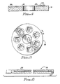
- Fig. 5 is a plan view of an electromagnetic pallet assembly.
- Fig. 6 is a section view taken along lines 6-6 of Fig. 5.
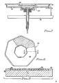
- Fig. 7 is a side view of the substrate electrode assembly with the electromagnetic pallet in operative position.
- Fig. 8 is a plan view of an alternate embodiment of the polygon-shaped planar coil.
- Fig. 9 is a section view taken along lines 8-8 of Fig. 7.
- Referring to Fig. 1, the general structure of the electrode assemblies and the power supply is shown for the sputtering apparatus according to the present invention. The
sputtering apparatus 10 of the invention comprises avacuum enclosure 12 and a vacuum pump (not shown) to evacuate the sputtering enclosure to a desired background pressure level. A suitable gas such as argon, for example, is then fed into the enclosure to provide the necessary background environment for sputter deposition. - A
target electrode assembly 14 to which a target body is mounted is positioned within theenclosure 12, and asubstrate electrode assembly 16 is positioned adjacent to and facing thetarget electrode assembly 14. The electrode assemblies 14 and 16 may be water cooled to maintain a desired temperature during operation. To eliminate spurious sputtering that may occur at the back of theelectrode assemblies electrode assembly ground shield 18 and 20, respectively, surrounding the peripheral and back portions of the electrode assembly, thereby leaving the face of the electrode assemblies exposed for supporting target bodies and substrates to be coated. - The
power supply 22 is connected to supply an RF voltage potential acrosstarget electrode assembly 14,substrate electrode assembly 16, andvariable impedance 24. The capacitive and inductive components ofvariable impedance 24 can be varied to control the voltage tosubstrate electrode assembly 16 to provide control over the properties of the films deposited by the sputtering apparatus. - According to the present invention, a novel structure for the
substrate electrode assembly 16, which will be described in detail below, enables the sputtering apparatus to produce thin magnetic films with uniform thickness across a substrate and from substrate to substrate while maintaining the easy axis orientation of the deposited films with great precision by means of the magnetic field generated by a planar electromagnetic coil. - In accordance with the present invention, the novel structure of the substrate electrode assembly is shown schematically in Figs. 2, 3, and 4. As shown in Fig. 2, a planar
electromagnetic coil 26 is provided, andcoil 26 has a plurality ofplanar sides 28.Coil 26 is a spiral coil so that when the coil is energized with a suitable voltage, a magnetic field is produced with the magnetization oriented normal to the coil which turns at each of theplanar sides 28 of the coil as shown byarrows 30. - As shown in Fig. 3, the planar
electromagnetic coil 26 is fixed in position at or near thesurface 32 ofsubstrate electrode assembly 16, and a plurality ofsubstrates 34 are positioned on thesubstrate electrode assembly 16. Thesubstrates 34 are positioned so that an edge is parallel to one of theplanar sides 28 of the planarelectromagnetic coil 26. The section view of the substrate electrode assembly, Fig. 4, shows that thesubstrates 34 are in close proximity to the planarelectromagnetic coil 26. The substrate electrode assembly is normally water cooled, but this structure is not included in the schematic showing of Fig. 4. This orientation of thesubstrates 34 enables a thin film of a magnetic material to be sputtered upon each of thesubstrates 34 with the easy axis oriented in a chosen direction to a very close tolerance. In addition, the thickness of the sputtered magnetic material is uniform to a very close tolerance over all the plurality ofsubstrates 34 since there is little interaction between the magnetic field produced bycoil 26 and the plasma when relative motion is produced between thetarget electrode assembly 14 and thesubstrate electrode assembly 16 during operation of the sputtering apparatus. - An alternate embodiment of the substrate electrode assembly is shown in Figs. 5 and 6. In this embodiment, the planar
electromagnetic coil 26 is embedded within anelectromagnetic pallet assembly 36, which also serves as a support for thesubstrates 38 during sputtering. Thecoil 26 is a spiral coil, and both ends of the coil are connected tocommutator rings 40 at the periphery of thepallet assembly 36 so that electrical contact can be maintained to the pallet assembly during rotation. - As shown in Fig. 7, the
electromagnetic pallet assembly 36 is mounted directly upon thesubstrate electrode assembly 16′, andcontactors 42 are fixed tovacuum enclosure baseplate 44 and extend into a position to provide electrical contact tocommutator rings 40 so that the planarelectromagnetic coil 26 can be energized during rotation of thesubstrate electrode assembly 16′. Thesubstrates 38 can be loaded onto the electromagnetic pallet assembly outside the sputtering apparatus, and loaded along with theelectromagnetic pallet assembly 36. - An alternate embodiment of the planar electromagnetic coil is shown in Figs. 8 and 9. In this embodiment, the planar
electromagnetic coil 26′ is produced by photolithographic techniques to produce a polygon-shapedplanar coil 26′ on one surface of the substrate 46. The substrate 46 may comprise any suitable dielectric material such as fiberglass-filled epoxy, for example. Adielectric coating 48 is provided on top of thecoil 26′, and this coating may comprise an epoxy resin, for example. - The production of the coil by photolithographic techniques permits the coil to be produced with greater accuracy at lower cost. In addition, if desired, the coil can be produced in a plurality of layers. Each of the layers is connected in parallel so that a greater field strength can be produced by the same current as that required for the single-layer coil or, alternatively, a lower current can be used to produce the same field strength as that produced by the single-layer coil. The connection of the plurality of layers in parallel produces a lower resistance, while permitting a higher magnetic field due to the increased ampere turns. This results in lower heat dissipation for the coil due to the lower resistance from the parallel connection.
Claims (6)
- sputtering apparatus (10) for coating a substrate (34) with a magnetic material having an axis oriented in a chosen direction comprising:a first electrode (14) for supporting a suitable target material;a second electrode (16, 16′) for supporting at least one substrate (34) adjacent to and in alignment with said first electrode; characterized by said second electrode having a polygon-shaped planar coil (26; 26′) adjacent a surface thereof and means for energizing said coil to form a uniform magnetic field on said surface oriented substantially normal to the polygon faces of said coil;a source (22) of RF power arranged to impose an RF voltage across said first and said second electrodes to produce a glow discharge in the space between said first and said second electrodes; andmeans for producing relative motion between said first and said second electrodes in a plane parallel to said planar coil whereby a uniform coating of magnetic material can be deposited on a substrate supported on said second electrode with the coating of magnetic material having an axis oriented in a chosen direction.
- The sputtering apparatus as claimed in claim 1, wherein said polygon-shaped planar coil (26; 26′) is embedded within said second electrode.
- The sputtering apparatus as claimed in claim 1, additionally comprising:a pallet member (36); andmeans for incorporating said polygon-shaped planar coil into said pallet member.
- The sputtering apparatus as claimed in any preceding claim comprising a plurality of substrates (34), each oriented with a reference edge parallel to one of said polygon faces of said polygon-shaped planar coil.
- The sputtering apparatus of claim 4, wherein said polygon-shaped planar coil is formed by photolithographic techniques.
- A polygon-shaped planar coil formed by photolithographic technique.
Applications Claiming Priority (2)
| Application Number | Priority Date | Filing Date | Title |
|---|---|---|---|
| US07/452,984 US5026470A (en) | 1989-12-19 | 1989-12-19 | Sputtering apparatus |
| US452984 | 1989-12-19 |
Publications (2)
| Publication Number | Publication Date |
|---|---|
| EP0435838A2 true EP0435838A2 (en) | 1991-07-03 |
| EP0435838A3 EP0435838A3 (en) | 1991-10-02 |
Family
ID=23798757
Family Applications (1)
| Application Number | Title | Priority Date | Filing Date |
|---|---|---|---|
| EP19900850412 Withdrawn EP0435838A3 (en) | 1989-12-19 | 1990-12-17 | Sputtering apparatus |
Country Status (3)
| Country | Link |
|---|---|
| US (1) | US5026470A (en) |
| EP (1) | EP0435838A3 (en) |
| JP (1) | JPH03191060A (en) |
Cited By (6)
| Publication number | Priority date | Publication date | Assignee | Title |
|---|---|---|---|---|
| EP0479189A1 (en) * | 1990-09-29 | 1992-04-08 | Tokyo Electron Limited | Magnetron plasma processing apparatus |
| EP0470580A3 (en) * | 1990-08-07 | 1992-04-15 | Canon Kabushiki Kaisha | Plasma processing apparatus |
| US5316645A (en) * | 1990-08-07 | 1994-05-31 | Canon Kabushiki Kaisha | Plasma processing apparatus |
| DE19643841A1 (en) * | 1996-10-30 | 1998-05-07 | Balzers Prozess Systeme Gmbh | Device for coating substrates, in particular with magnetizable materials |
| RU2186151C2 (en) * | 1999-12-29 | 2002-07-27 | Закрытое акционерное общество "Патинор Коутингс Лимитед" | Device for application of coatings in vacuum |
| DE19981147B4 (en) * | 1998-05-22 | 2008-07-31 | Cvc Products, Inc. | A substrate holding assembly for supporting a substrate in a substrate processing environment |
Families Citing this family (21)
| Publication number | Priority date | Publication date | Assignee | Title |
|---|---|---|---|---|
| US5130005A (en) * | 1990-10-31 | 1992-07-14 | Materials Research Corporation | Magnetron sputter coating method and apparatus with rotating magnet cathode |
| CA2061119C (en) * | 1991-04-19 | 1998-02-03 | Pei-Ing P. Lee | Method of depositing conductors in high aspect ratio apertures |
| JP2725944B2 (en) * | 1991-04-19 | 1998-03-11 | インターナショナル・ビジネス・マシーンズ・コーポレイション | Metal layer deposition method |
| US5300813A (en) * | 1992-02-26 | 1994-04-05 | International Business Machines Corporation | Refractory metal capped low resistivity metal conductor lines and vias |
| DE69325959T2 (en) * | 1992-08-24 | 2000-04-20 | Matsushita Electric Industrial Co., Ltd. | Manufacturing process of a soft magnetic film |
| US6491802B2 (en) | 1992-10-28 | 2002-12-10 | Hitachi, Ltd. | Magnetic film forming system |
| JPH0822367B2 (en) * | 1992-11-27 | 1996-03-06 | 富士通株式会社 | Gas purification equipment |
| US5630916A (en) * | 1993-03-02 | 1997-05-20 | Cvc Products, Inc. | Magnetic orienting device for thin film deposition and method of use |
| JP4355036B2 (en) * | 1997-03-18 | 2009-10-28 | キヤノンアネルバ株式会社 | Ionization sputtering equipment |
| JPH111770A (en) * | 1997-06-06 | 1999-01-06 | Anelva Corp | Sputtering apparatus and sputtering method |
| US6249200B1 (en) * | 1998-04-10 | 2001-06-19 | Dexter Magnetic Technologies, Inc. | Combination of magnets for generating a uniform external magnetic field |
| US6042707A (en) * | 1998-05-22 | 2000-03-28 | Cvc Products, Inc. | Multiple-coil electromagnet for magnetically orienting thin films |
| US6545580B2 (en) | 1998-09-09 | 2003-04-08 | Veeco Instruments, Inc. | Electromagnetic field generator and method of operation |
| US6579421B1 (en) | 1999-01-07 | 2003-06-17 | Applied Materials, Inc. | Transverse magnetic field for ionized sputter deposition |
| US8696875B2 (en) * | 1999-10-08 | 2014-04-15 | Applied Materials, Inc. | Self-ionized and inductively-coupled plasma for sputtering and resputtering |
| US10047430B2 (en) | 1999-10-08 | 2018-08-14 | Applied Materials, Inc. | Self-ionized and inductively-coupled plasma for sputtering and resputtering |
| US6373364B1 (en) | 2000-02-03 | 2002-04-16 | Cvc Products, Inc. | Electromagnet for thin-film processing with winding pattern for reducing skew |
| US6402903B1 (en) | 2000-02-04 | 2002-06-11 | Steag Hamatech Ag | Magnetic array for sputtering system |
| US6914749B2 (en) * | 2000-07-25 | 2005-07-05 | Seagate Technology Llc | Magnetic anisotropy of soft-underlayer induced by magnetron field |
| EP1490527A1 (en) * | 2002-03-29 | 2004-12-29 | D2 In-Line Solutions, LLC | Gravity-fed in-line continuous processing system and method |
| US7504006B2 (en) * | 2002-08-01 | 2009-03-17 | Applied Materials, Inc. | Self-ionized and capacitively-coupled plasma for sputtering and resputtering |
Family Cites Families (9)
| Publication number | Priority date | Publication date | Assignee | Title |
|---|---|---|---|---|
| FR2324755A1 (en) * | 1975-09-19 | 1977-04-15 | Anvar | HIGH SPEED OF DEPOSIT CATHODIC SPRAY DEVICE |
| DE2735525A1 (en) * | 1977-08-06 | 1979-02-22 | Leybold Heraeus Gmbh & Co Kg | CATODE ARRANGEMENT WITH TARGET FOR SPRAYING SYSTEMS FOR DUSTING UP DIELECTRIC OR AMAGNETIC LAYERS ON SUBSTRATES |
| JPS5778123A (en) * | 1980-11-04 | 1982-05-15 | Hitachi Ltd | Manufacture of anisotropic thin magnetic film |
| DE3502770A1 (en) * | 1985-01-28 | 1986-07-31 | Siemens AG, 1000 Berlin und 8000 München | METHOD FOR PRODUCING A FLAT COIL AND FLAT COIL FOR A SHOCK SHAFT PIPE |
| JPS6254907A (en) * | 1985-09-04 | 1987-03-10 | Hitachi Ltd | sputtering device |
| JPS6274073A (en) * | 1985-09-26 | 1987-04-04 | Hitachi Ltd | Sputtering device |
| JPS6380841A (en) * | 1986-09-25 | 1988-04-11 | Canon Inc | plasma control device |
| JPS63317663A (en) * | 1987-06-19 | 1988-12-26 | Ube Ind Ltd | Plasma compression sputtering device and method |
| US4849250A (en) * | 1988-01-27 | 1989-07-18 | Storage Technology Corporation | Method and apparatus for producing magnetically oriented films on substrates |
-
1989
- 1989-12-19 US US07/452,984 patent/US5026470A/en not_active Expired - Fee Related
-
1990
- 1990-10-17 JP JP2276575A patent/JPH03191060A/en active Pending
- 1990-12-17 EP EP19900850412 patent/EP0435838A3/en not_active Withdrawn
Cited By (8)
| Publication number | Priority date | Publication date | Assignee | Title |
|---|---|---|---|---|
| EP0470580A3 (en) * | 1990-08-07 | 1992-04-15 | Canon Kabushiki Kaisha | Plasma processing apparatus |
| US5316645A (en) * | 1990-08-07 | 1994-05-31 | Canon Kabushiki Kaisha | Plasma processing apparatus |
| EP0479189A1 (en) * | 1990-09-29 | 1992-04-08 | Tokyo Electron Limited | Magnetron plasma processing apparatus |
| US5376211A (en) * | 1990-09-29 | 1994-12-27 | Tokyo Electron Limited | Magnetron plasma processing apparatus and processing method |
| DE19643841A1 (en) * | 1996-10-30 | 1998-05-07 | Balzers Prozess Systeme Gmbh | Device for coating substrates, in particular with magnetizable materials |
| US5922182A (en) * | 1996-10-30 | 1999-07-13 | Balzers Prozeb-Systeme Gmbh | Apparatus for coating substrates especially with magnetizable materials |
| DE19981147B4 (en) * | 1998-05-22 | 2008-07-31 | Cvc Products, Inc. | A substrate holding assembly for supporting a substrate in a substrate processing environment |
| RU2186151C2 (en) * | 1999-12-29 | 2002-07-27 | Закрытое акционерное общество "Патинор Коутингс Лимитед" | Device for application of coatings in vacuum |
Also Published As
| Publication number | Publication date |
|---|---|
| US5026470A (en) | 1991-06-25 |
| EP0435838A3 (en) | 1991-10-02 |
| JPH03191060A (en) | 1991-08-21 |
Similar Documents
| Publication | Publication Date | Title |
|---|---|---|
| US5026470A (en) | Sputtering apparatus | |
| US6235164B1 (en) | Low-pressure processing system for magnetic orientation of thin magnetic film | |
| US4842703A (en) | Magnetron cathode and method for sputter coating | |
| JP3516054B2 (en) | Apparatus for generating plasma by cathodic sputtering | |
| US5589039A (en) | In-plane parallel bias magnetic field generator for sputter coating magnetic materials onto substrates | |
| JP2000144399A (en) | Sputtering equipment | |
| US5232569A (en) | Circularly symmetric, large-area, high-deposition-rate sputtering apparatus for the coating of disk substrates | |
| KR20070008369A (en) | Magnetron Sputtering System for Large Area Boards | |
| US5891311A (en) | Sputter coating system and method using substrate electrode | |
| US5397448A (en) | Device for generating a plasma by means of cathode sputtering and microwave-irradiation | |
| GB2310433A (en) | Cathode sputtering | |
| CN115449763B (en) | Fan-shaped magnet structure for magnetron sputtering and magnetron sputtering equipment | |
| US5753089A (en) | Sputter coating station | |
| US5540823A (en) | Magnetron cathode | |
| JP3411312B2 (en) | Magnetron sputter cathode and method of adjusting film thickness distribution | |
| US7294242B1 (en) | Collimated and long throw magnetron sputtering of nickel/iron films for magnetic recording head applications | |
| US5198090A (en) | Sputtering apparatus for producing thin films of material | |
| JP2000319780A (en) | Sputtering cathode and magnetron type sputtering apparatus provided with the same | |
| EP0474348B1 (en) | Sputtering apparatus and method for producing thin films of material | |
| KR100963413B1 (en) | Magnetron sputtering device | |
| JPH0517869A (en) | Sputtering method and device | |
| JP2756912B2 (en) | Magnetic field generator for magnetron plasma | |
| US5403663A (en) | Process for coating a polycarbonate substrate with an aluminum-silicon alloy | |
| JPS61288067A (en) | Sputtering device | |
| JP2789251B2 (en) | Sputtering equipment using dipole ring type magnetic circuit |
Legal Events
| Date | Code | Title | Description |
|---|---|---|---|
| PUAI | Public reference made under article 153(3) epc to a published international application that has entered the european phase |
Free format text: ORIGINAL CODE: 0009012 |
|
| AK | Designated contracting states |
Kind code of ref document: A2 Designated state(s): DE FR GB |
|
| PUAL | Search report despatched |
Free format text: ORIGINAL CODE: 0009013 |
|
| AK | Designated contracting states |
Kind code of ref document: A3 Designated state(s): DE FR GB |
|
| 17P | Request for examination filed |
Effective date: 19911018 |
|
| STAA | Information on the status of an ep patent application or granted ep patent |
Free format text: STATUS: THE APPLICATION HAS BEEN WITHDRAWN |
|
| 18W | Application withdrawn |
Withdrawal date: 19920905 |