EP0435686B1 - Contact sensor module - Google Patents
Contact sensor module Download PDFInfo
- Publication number
- EP0435686B1 EP0435686B1 EP90314383A EP90314383A EP0435686B1 EP 0435686 B1 EP0435686 B1 EP 0435686B1 EP 90314383 A EP90314383 A EP 90314383A EP 90314383 A EP90314383 A EP 90314383A EP 0435686 B1 EP0435686 B1 EP 0435686B1
- Authority
- EP
- European Patent Office
- Prior art keywords
- contacts
- contact sensor
- transformer
- sensing
- loop
- Prior art date
- Legal status (The legal status is an assumption and is not a legal conclusion. Google has not performed a legal analysis and makes no representation as to the accuracy of the status listed.)
- Expired - Lifetime
Links
- 238000002955 isolation Methods 0.000 claims abstract description 11
- 238000004519 manufacturing process Methods 0.000 claims abstract description 5
- 230000005291 magnetic effect Effects 0.000 claims description 6
- 238000006243 chemical reaction Methods 0.000 abstract description 2
- 239000003990 capacitor Substances 0.000 description 3
- 238000002844 melting Methods 0.000 description 3
- 230000008018 melting Effects 0.000 description 3
- 238000000034 method Methods 0.000 description 3
- 230000005855 radiation Effects 0.000 description 3
- 239000004020 conductor Substances 0.000 description 2
- 238000010586 diagram Methods 0.000 description 2
- 230000000694 effects Effects 0.000 description 2
- 230000001105 regulatory effect Effects 0.000 description 2
- 239000004593 Epoxy Substances 0.000 description 1
- 230000003213 activating effect Effects 0.000 description 1
- 230000002457 bidirectional effect Effects 0.000 description 1
- 230000008878 coupling Effects 0.000 description 1
- 238000010168 coupling process Methods 0.000 description 1
- 238000005859 coupling reaction Methods 0.000 description 1
- 230000007613 environmental effect Effects 0.000 description 1
- 238000001914 filtration Methods 0.000 description 1
- 230000036039 immunity Effects 0.000 description 1
- 238000009434 installation Methods 0.000 description 1
- 230000005693 optoelectronics Effects 0.000 description 1
- 230000010355 oscillation Effects 0.000 description 1
- 230000001052 transient effect Effects 0.000 description 1
- 238000004804 winding Methods 0.000 description 1
Images

Classifications
-
- H—ELECTRICITY
- H01—ELECTRIC ELEMENTS
- H01H—ELECTRIC SWITCHES; RELAYS; SELECTORS; EMERGENCY PROTECTIVE DEVICES
- H01H9/00—Details of switching devices, not covered by groups H01H1/00 - H01H7/00
- H01H9/16—Indicators for switching condition, e.g. "on" or "off"
- H01H9/167—Circuits for remote indication
Definitions
- the present invention relates to contact sensors for relays, limit switches and various types of electrical, mechanical, magnetic, pneumatic and other devices having contacts that open and close and that require electrical and/or electronic circuitry for the sensing of the state of the sets of contacts (open or closed), being also more particularly directed to contact sensors compatible with I/O (input-output) modules of the type employed in isolated interfacing between microprocessors and industrial processes.
- I/O input-output
- Such isolated interfacing between microprocessors and industrial processes is currently standardised by the use of a plug compatible I/O system, such as that of Opto 22 of Huntington Beach, California, as described, for example, in their current "Microprocessor I/O Systems Catalogue".
- the standard defines a universal mounting rack that provides system termination for groups of 4,8,16 or 24 plug-in modules. There is a module type for each of four different functions; switches for AC or DC outputs and sensors for AC or DC inputs.
- the I/O modules are constructed by sliding a printed circuit board with pins along one edge into a plastic housing (like a cup, with pins protruding about the rim) and then filling with epoxy.
- the inverted housing then becomes a colour-coded module with 4 or 5 pins spaced along its bottom.
- the modules in turn, are plugged into a universal mounting rack and secured in place by tightening a screw which is held captive in the module assembly.
- the rack makes connections to the pins of the modules and provides two screw terminals for field wiring termination (one fused), and three connections to the microprocessor system. These three connections are, customarily, supply voltage (+5 volts run through an LED indicator on the rack), a signal line (a bidirectional line with 3300 ohms to the +5 volts) and a common ground line. (See, for example, Grayhill 1988 catalogue sheet "8 Modules Rack” 70RCK8).
- an output from a microprocessor pulls current from the signal pin in order to actuate the isolated switch that is connected in circuit across the user terminals.
- An input module is just the reverse; the flow of current across an isolated sensing/switching device connected in circuit across the user terminal activating a switch that pulls current from the signal pin and changes the state of a microprocessor input.
- the racks and modules provide all of the interfacing hardware needed to connect a microprocessor system to a process.
- EP-A-0 204 624 discloses a contact sensor module according to the preamble of claim 1.
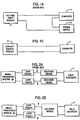
- Figs 1A and 1B of which are generic wiring drawings respectively of the prior art existing contact sensor loop and the improved and simplified loop of the present invention
- Fig 1A the before-mentioned additional power supply of presently used techniques is shown at 3 in the wired installation loop with, for example, voltage input module 5 and with the field contacts of the relay, limit switch or other device, schematically shown at 1. If the contacts are open (off state), the same are not apparent to the input module 5; but if the contacts are closed, voltage is applied to the input module.
- a single module is employed at 2 that both powers the loop and senses the state of the contacts - a so-called contact sensor module, applying a current-limited voltage to the contacts which, when closed, enables sensing of the pulling or reverse current.
- Such a module eliminates the need for a separate power supply, all the fuses and the mass distribution terminals. Even more importantly, it dramatically reduces the wiring complexity and cost, using a single two-conductor wire in a simple point-to-point connection.
- such a single isolation device 2" is preferably a transformer driven by an oscillator, transporting the power and sensing the reflected impedance to provide the logical signal. Sensing the logic signal through the magnetic isolation of the transformer requires much less loop current than the conventional optoelectronic approach such that less power is required from the isolated, high-voltage loop source. Allowing low power and high frequency operation, moreover, permits the design of a transformer that will fit within the physical constraints afforded by the standard Opto 22 or other module.
- a further feature involved in this isolation transformer use is the idea of converting the output of the transformer from AC to DC before it is connected to the loop.
- DC By powering the loop with DC, the effects of stray capacitance are eliminated.
- AC powered loops must use a low modulation frequency in order to prevent RF radiation (in compliance with FCC rules), which would necessitate a transformer too large to fit into the standard module. Conversion to DC, therefore, makes the design possible and further allows for the use of capacitors to store energy that can be used in melting away contact oxides.
- resonant flyback pulses as a means of stepping up the transformer primary drive voltage without drawing additional power from the source, furthermore, can yield a sinusoidal waveform in the transformer that contributes to meeting FCC regulations pertaining to EMI radiated emissions.
- the single isolation device 2 (Fig 2B) is implemented as a standard T1 Carrier communications transformer, which is the only component needed to isolate the sensing loop power as well as the loop sense digital logic signal.
- T1 is a communications standard developed by Bell Labs in the late 1960's and is now a commonly used 1.544 MHz standard, so that the isolation device is readily available and cost effective.
- a preferred particular transformer used for this design has a split 1:2 winding arrangement (ie a one-to-two signal splitter).
- An example of a suitable transformer is the AIE Magnetics (of Russia, FL) part no 318-0696.
- the before-mentioned driving oscillator is shown at M1 and may be a timer chip such as a CMOS version of a 555 timer, tuned to run at about 100 Hz (R4 and C4 set the frequency).
- Its open drain output directly drives the transformer primary (pins "1" and "2") in a resonant mode; that is, while on, the switch pulls current through the primary and builds up a magnetic field in the core of T1.
- the primary tends to fly back to a very high voltage while the magnetic field collapses in the core.
- the flyback is a half-cycle sine wave (resonant-mode) and is therfore limited to only about 12 to 15 volts.
- the zener diode Z1 shown connected between pin "1" of M1 and the lower terminal "2" of the primary of T1, is added to protect M1 from unusually high flyback spikes caused by output transients. This technique of flyback is used as a means of boosting the output voltage while the sine wave eliminates harmonics and greatly limits any EMI radiation.
- the output of the transformer T1 is rectified by diodes D1 and D2, with the resulting DC voltage stored in capacitors C7 and C8 connected across the relay or limit switch or other field contacts 1 that are to be powered and condition-sensed in accordance with the invention.
- the absence of AC on the field wiring to the contacts 1 eliminates any possibility of emitted radiation and interference with other equipment from these wires.
- Sensing a DC load moreover, eliminates any effect of wiring or contact capacitance on the sensing threshold levels and switching operation.
- the DC voltage stored in the capacitors C7 and C8, furthermore, provides a mechanism of storing energy used in melting contact oxides and achieving good electrical conductivity upon contact closure of the contacts 1.
- Such a practical contact sensor module useful as an industry standard and adapted to co-exist with the Opto 22 or other standard I/O system 5 may have the following specifications:
- Fig 3 The implementation of Fig 3 has been found to meet the following specification and performance criteria.
- Supply current through the LED on the universal I/O rack 5 is a small 0.5 mA when contacts 1 are open and a much larger 9.9 mA when the contacts are closed.
- the open circuit voltage for the contact interface is 26 V.
- the short circuit current through the contacts is 2.1 mA.
- the contact circuit threshold resistance at which point the sensor or detector Q2 changes state is 37 Kohms.
- the turn on time is 0.2 mS and the turn off time is 1.3 mS.
- the galvanic isolation limit from the contact circuit 1 to the I/O rack circuit 5 is 500 VDC.
- the circuit meets all environmental requirements and all applicable regulatory requirements as previously described and requires no power or conductors therefor other than that normally provided in typical input-type modulators.
Landscapes
- Electronic Switches (AREA)
- Investigating Or Analyzing Materials By The Use Of Fluid Adsorption Or Reactions (AREA)
- Measurement Of Length, Angles, Or The Like Using Electric Or Magnetic Means (AREA)
- Arrangements For Transmission Of Measured Signals (AREA)
- Dc-Dc Converters (AREA)
Abstract
Description
Claims (8)
- A contact sensor module for sensing the open or closed state of a set of contacts of a relay limit switch and other switching devices comprising a single modele (2) directly connected in a single loop to a set of contacts (1), providing self-powering and sensing of the contacts in the loop, containing an oscillator (M1) and a transformer (T1), the oscillator (M1) powering the contacts (1) via the transformer (T1) characterised in sensing means (R1, Q1, Q2) located in the circuit that supplies power to the oscillator (M1), the sensing means (R1, Q1, Q2) sensing differences in the supply current to the oscillator (M1) and thereby the state of the contacts (1).
- A contact sensor module as claimed in claim 1 wherein said sensing means responds to the impedance reflected in the loop by the state of the contacts and generates a logical signal corresponding to the contact state.
- A contact sensor module as claimed in claim 2 wherein the module (2) is connected between an I/O system and the contacts (1) to interface between a microprocessor and an industrial process.
- A contact sensor as claimed in claim 3 wherein means is provided in said loop for electrically isolating the input-to-output circuits of the loop.
- A contact sensor as claimed in claim 4 wherein said transformer (T1) provides magnetic isolation that reduces loop current requirements.
- A contact sensor as claimed in claim 5 wherein the transformer (T1) is driven by a high frequency oscillator (M1) transporting the power and sensing the reflected impedance to provide said logical signal.
- A contact sensor as claimed in claim 6 wherein rectifying (D1, D2) and storage means (C7, C8) are provided between the output of the transformer (T1) and the set of contacts (1) to enable DC connections to power the contacts.
- A contact sensor as claimed in claim 6 wherein resonant flyback means (C5, C6, Z1) are connected to step up the drive of the primary of the transformer (T1) without an additional power requirement.
Applications Claiming Priority (2)
| Application Number | Priority Date | Filing Date | Title |
|---|---|---|---|
| US458888 | 1989-12-29 | ||
| US07/458,888 US5083116A (en) | 1989-12-29 | 1989-12-29 | Contact sensing module embodying loop power supply and state sensing for relays and other contacts |
Publications (3)
| Publication Number | Publication Date |
|---|---|
| EP0435686A2 EP0435686A2 (en) | 1991-07-03 |
| EP0435686A3 EP0435686A3 (en) | 1992-07-01 |
| EP0435686B1 true EP0435686B1 (en) | 1998-09-09 |
Family
ID=23822492
Family Applications (1)
| Application Number | Title | Priority Date | Filing Date |
|---|---|---|---|
| EP90314383A Expired - Lifetime EP0435686B1 (en) | 1989-12-29 | 1990-12-28 | Contact sensor module |
Country Status (5)
| Country | Link |
|---|---|
| US (1) | US5083116A (en) |
| EP (1) | EP0435686B1 (en) |
| JP (1) | JPH04315722A (en) |
| AT (1) | ATE171009T1 (en) |
| DE (1) | DE69032643D1 (en) |
Cited By (1)
| Publication number | Priority date | Publication date | Assignee | Title |
|---|---|---|---|---|
| DE102012102766B3 (en) * | 2012-03-30 | 2013-09-05 | Sma Solar Technology Ag | Emergency power system and grounding device for a network backup system |
Families Citing this family (8)
| Publication number | Priority date | Publication date | Assignee | Title |
|---|---|---|---|---|
| JPH0555435U (en) * | 1991-12-26 | 1993-07-23 | サンクス株式会社 | Output switch status detection circuit |
| FR2828005B1 (en) * | 2001-07-27 | 2003-09-26 | Delphi Tech Inc | INDUCTIVE COUPLING SWITCH |
| US20050035767A1 (en) * | 2003-08-11 | 2005-02-17 | Hardy William Dean | Plug detector for an electrical test instrument |
| US7654857B2 (en) * | 2007-08-14 | 2010-02-02 | Fluke Corporation | Digital multimeter having sealed input jack detection arrangement |
| US8901915B2 (en) | 2012-01-11 | 2014-12-02 | Elster Solutions, Llc | Voltage or contact closure sensor |
| GB2525206A (en) * | 2014-04-15 | 2015-10-21 | Bae Systems Plc | Circuit state sensing |
| US10374597B2 (en) * | 2014-04-15 | 2019-08-06 | Bae Systems Plc | Circuit state sensing |
| CN110767501B (en) * | 2019-09-27 | 2021-10-22 | 浙江工商职业技术学院 | A drive circuit of an energy-saving relay suitable for wide-voltage operation |
Family Cites Families (7)
| Publication number | Priority date | Publication date | Assignee | Title |
|---|---|---|---|---|
| DE1154554B (en) * | 1962-02-23 | 1963-09-19 | Licentia Gmbh | Arrangement for achieving reliable contact with a mechanical contact arrangement |
| FR2381384A1 (en) * | 1977-02-18 | 1978-09-15 | Crouzet Sa | Tester for conductance of electromechanical contact - has transformer secondary winding which can be short circuited by contact |
| US4376277A (en) * | 1980-10-17 | 1983-03-08 | Honeywell Inc. | Dynamic contact checking circuit |
| JPS58140922A (en) * | 1982-02-17 | 1983-08-20 | 株式会社日立製作所 | Contact signal input circuit for electronic controller |
| GB2159285B (en) * | 1984-05-11 | 1987-10-14 | Cambridge Instr Ltd | Circuit monitor |
| FR2582880B1 (en) * | 1985-05-30 | 1992-11-27 | Matra | DEVICE FOR MONITORING THE STATE OF AN ELECTRIC SWITCH AND ELECTRIC RELAY COMPRISING AN APPLICATION |
| DE3717260A1 (en) * | 1987-05-22 | 1988-12-01 | Rexroth Mannesmann Gmbh | CIRCUIT ARRANGEMENT FOR TRANSMITTING A SUPPLY VOLTAGE AND A CONTROL SIGNAL |
-
1989
- 1989-12-29 US US07/458,888 patent/US5083116A/en not_active Expired - Fee Related
-
1990
- 1990-12-28 AT AT90314383T patent/ATE171009T1/en not_active IP Right Cessation
- 1990-12-28 DE DE69032643T patent/DE69032643D1/en not_active Expired - Lifetime
- 1990-12-28 JP JP2409250A patent/JPH04315722A/en active Pending
- 1990-12-28 EP EP90314383A patent/EP0435686B1/en not_active Expired - Lifetime
Cited By (2)
| Publication number | Priority date | Publication date | Assignee | Title |
|---|---|---|---|---|
| DE102012102766B3 (en) * | 2012-03-30 | 2013-09-05 | Sma Solar Technology Ag | Emergency power system and grounding device for a network backup system |
| WO2013144316A1 (en) | 2012-03-30 | 2013-10-03 | Sma Solar Technology Ag | Backup power system and grounding device for a backup power system |
Also Published As
| Publication number | Publication date |
|---|---|
| DE69032643D1 (en) | 1998-10-15 |
| EP0435686A2 (en) | 1991-07-03 |
| US5083116A (en) | 1992-01-21 |
| EP0435686A3 (en) | 1992-07-01 |
| JPH04315722A (en) | 1992-11-06 |
| ATE171009T1 (en) | 1998-09-15 |
Similar Documents
| Publication | Publication Date | Title |
|---|---|---|
| US5065104A (en) | Fault sensing with an artificial reference potential provided by an isolated capacitance effect | |
| US5270576A (en) | Electrical connector network | |
| US4833563A (en) | Molded case circuit breaker actuator-accessory module | |
| US4788621A (en) | Molded case circuit breaker multiple accessory unit | |
| EP0962081B1 (en) | Logic isolator with high transient immunity | |
| EP3618279B1 (en) | Output module and corresponding method for industrial control | |
| US4890184A (en) | Molded case circuit breaker actuator-accessory unit | |
| US5083116A (en) | Contact sensing module embodying loop power supply and state sensing for relays and other contacts | |
| US5347418A (en) | Fuse blowout detector circuit | |
| JPS63253867A (en) | Dc-dc power converter | |
| US3866051A (en) | Digital interface module | |
| US5444309A (en) | Reduced wattage PLC interface | |
| US6556406B1 (en) | Solid-state relay | |
| CN102841254B (en) | The phase bit comparison equipment of system power supply | |
| JPS62501601A (en) | power switch | |
| US4864156A (en) | Proximity switch with noncontact effect | |
| KR930012135B1 (en) | Electronic bipolar interface circuit | |
| US5760499A (en) | Safety device for socket which is connected to electrical power supply | |
| JPH02219417A (en) | Overvoltage protective circuit | |
| SU1026226A2 (en) | Device for overvoltage and undervoltage protection of electric device | |
| GB2091957A (en) | Voltage converter | |
| US20110193424A1 (en) | System comprising a plurality of controllers and associated method | |
| US4025822A (en) | Two to three-wire converter circuit | |
| JPH0755153Y2 (en) | Switch circuit | |
| JPH07295608A (en) | Input circuit |
Legal Events
| Date | Code | Title | Description |
|---|---|---|---|
| PUAI | Public reference made under article 153(3) epc to a published international application that has entered the european phase |
Free format text: ORIGINAL CODE: 0009012 |
|
| AK | Designated contracting states |
Kind code of ref document: A2 Designated state(s): AT BE CH DE DK ES FR GB GR IT LI NL SE |
|
| PUAL | Search report despatched |
Free format text: ORIGINAL CODE: 0009013 |
|
| AK | Designated contracting states |
Kind code of ref document: A3 Designated state(s): AT BE CH DE DK ES FR GB GR IT LI NL SE |
|
| 17P | Request for examination filed |
Effective date: 19921209 |
|
| 17Q | First examination report despatched |
Effective date: 19950210 |
|
| GRAG | Despatch of communication of intention to grant |
Free format text: ORIGINAL CODE: EPIDOS AGRA |
|
| GRAG | Despatch of communication of intention to grant |
Free format text: ORIGINAL CODE: EPIDOS AGRA |
|
| GRAH | Despatch of communication of intention to grant a patent |
Free format text: ORIGINAL CODE: EPIDOS IGRA |
|
| GRAH | Despatch of communication of intention to grant a patent |
Free format text: ORIGINAL CODE: EPIDOS IGRA |
|
| GRAA | (expected) grant |
Free format text: ORIGINAL CODE: 0009210 |
|
| AK | Designated contracting states |
Kind code of ref document: B1 Designated state(s): AT BE CH DE DK ES FR GB GR IT LI NL SE |
|
| PG25 | Lapsed in a contracting state [announced via postgrant information from national office to epo] |
Ref country code: IT Free format text: LAPSE BECAUSE OF FAILURE TO SUBMIT A TRANSLATION OF THE DESCRIPTION OR TO PAY THE FEE WITHIN THE PRE;WARNING: LAPSES OF ITALIAN PATENTS WITH EFFECTIVE DATE BEFORE 2007 MAY HAVE OCCURRED AT ANY TIME BEFORE 2007. THE CORRECT EFFECTIVE DATE MAY BE DIFFERENT FROM THE ONE RECORDED.SCRIBED TIME-LIMIT Effective date: 19980909 Ref country code: CH Free format text: LAPSE BECAUSE OF FAILURE TO SUBMIT A TRANSLATION OF THE DESCRIPTION OR TO PAY THE FEE WITHIN THE PRESCRIBED TIME-LIMIT Effective date: 19980909 Ref country code: FR Free format text: LAPSE BECAUSE OF FAILURE TO SUBMIT A TRANSLATION OF THE DESCRIPTION OR TO PAY THE FEE WITHIN THE PRESCRIBED TIME-LIMIT Effective date: 19980909 Ref country code: NL Free format text: LAPSE BECAUSE OF FAILURE TO SUBMIT A TRANSLATION OF THE DESCRIPTION OR TO PAY THE FEE WITHIN THE PRESCRIBED TIME-LIMIT Effective date: 19980909 Ref country code: LI Free format text: LAPSE BECAUSE OF FAILURE TO SUBMIT A TRANSLATION OF THE DESCRIPTION OR TO PAY THE FEE WITHIN THE PRESCRIBED TIME-LIMIT Effective date: 19980909 Ref country code: AT Free format text: LAPSE BECAUSE OF FAILURE TO SUBMIT A TRANSLATION OF THE DESCRIPTION OR TO PAY THE FEE WITHIN THE PRESCRIBED TIME-LIMIT Effective date: 19980909 Ref country code: GR Free format text: LAPSE BECAUSE OF NON-PAYMENT OF DUE FEES Effective date: 19980909 Ref country code: ES Free format text: THE PATENT HAS BEEN ANNULLED BY A DECISION OF A NATIONAL AUTHORITY Effective date: 19980909 Ref country code: BE Free format text: LAPSE BECAUSE OF FAILURE TO SUBMIT A TRANSLATION OF THE DESCRIPTION OR TO PAY THE FEE WITHIN THE PRESCRIBED TIME-LIMIT Effective date: 19980909 |
|
| REF | Corresponds to: |
Ref document number: 171009 Country of ref document: AT Date of ref document: 19980915 Kind code of ref document: T |
|
| REG | Reference to a national code |
Ref country code: CH Ref legal event code: EP |
|
| REF | Corresponds to: |
Ref document number: 69032643 Country of ref document: DE Date of ref document: 19981015 |
|
| PG25 | Lapsed in a contracting state [announced via postgrant information from national office to epo] |
Ref country code: SE Free format text: LAPSE BECAUSE OF FAILURE TO SUBMIT A TRANSLATION OF THE DESCRIPTION OR TO PAY THE FEE WITHIN THE PRESCRIBED TIME-LIMIT Effective date: 19981209 Ref country code: DK Free format text: LAPSE BECAUSE OF FAILURE TO SUBMIT A TRANSLATION OF THE DESCRIPTION OR TO PAY THE FEE WITHIN THE PRESCRIBED TIME-LIMIT Effective date: 19981209 |
|
| PG25 | Lapsed in a contracting state [announced via postgrant information from national office to epo] |
Ref country code: DE Free format text: LAPSE BECAUSE OF FAILURE TO SUBMIT A TRANSLATION OF THE DESCRIPTION OR TO PAY THE FEE WITHIN THE PRESCRIBED TIME-LIMIT Effective date: 19981210 |
|
| PG25 | Lapsed in a contracting state [announced via postgrant information from national office to epo] |
Ref country code: GB Free format text: LAPSE BECAUSE OF NON-PAYMENT OF DUE FEES Effective date: 19981228 |
|
| NLV1 | Nl: lapsed or annulled due to failure to fulfill the requirements of art. 29p and 29m of the patents act | ||
| EN | Fr: translation not filed | ||
| REG | Reference to a national code |
Ref country code: CH Ref legal event code: PL |
|
| PLBE | No opposition filed within time limit |
Free format text: ORIGINAL CODE: 0009261 |
|
| STAA | Information on the status of an ep patent application or granted ep patent |
Free format text: STATUS: NO OPPOSITION FILED WITHIN TIME LIMIT |
|
| GBPC | Gb: european patent ceased through non-payment of renewal fee |
Effective date: 19981228 |
|
| 26N | No opposition filed |