EP0434318A2 - Diffundierte Kontakte mit niedriger Schichtwiderstand für vergrabene diffundierte Widerstand unter Verwendung von Isolationszonen und einer vergrabenen Zone - Google Patents
Diffundierte Kontakte mit niedriger Schichtwiderstand für vergrabene diffundierte Widerstand unter Verwendung von Isolationszonen und einer vergrabenen Zone Download PDFInfo
- Publication number
- EP0434318A2 EP0434318A2 EP90313684A EP90313684A EP0434318A2 EP 0434318 A2 EP0434318 A2 EP 0434318A2 EP 90313684 A EP90313684 A EP 90313684A EP 90313684 A EP90313684 A EP 90313684A EP 0434318 A2 EP0434318 A2 EP 0434318A2
- Authority
- EP
- European Patent Office
- Prior art keywords
- substrate
- conductivity type
- leadouts
- buried layer
- contact
- Prior art date
- Legal status (The legal status is an assumption and is not a legal conclusion. Google has not performed a legal analysis and makes no representation as to the accuracy of the status listed.)
- Withdrawn
Links
Images

Classifications
-
- H—ELECTRICITY
- H10—SEMICONDUCTOR DEVICES; ELECTRIC SOLID-STATE DEVICES NOT OTHERWISE PROVIDED FOR
- H10W—GENERIC PACKAGES, INTERCONNECTIONS, CONNECTORS OR OTHER CONSTRUCTIONAL DETAILS OF DEVICES COVERED BY CLASS H10
- H10W20/00—Interconnections in chips, wafers or substrates
- H10W20/01—Manufacture or treatment
- H10W20/021—Manufacture or treatment of interconnections within wafers or substrates
-
- H—ELECTRICITY
- H10—SEMICONDUCTOR DEVICES; ELECTRIC SOLID-STATE DEVICES NOT OTHERWISE PROVIDED FOR
- H10D—INORGANIC ELECTRIC SEMICONDUCTOR DEVICES
- H10D48/00—Individual devices not covered by groups H10D1/00 - H10D44/00
- H10D48/50—Devices controlled by mechanical forces, e.g. pressure
-
- H—ELECTRICITY
- H10—SEMICONDUCTOR DEVICES; ELECTRIC SOLID-STATE DEVICES NOT OTHERWISE PROVIDED FOR
- H10D—INORGANIC ELECTRIC SEMICONDUCTOR DEVICES
- H10D62/00—Semiconductor bodies, or regions thereof, of devices having potential barriers
- H10D62/10—Shapes, relative sizes or dispositions of the regions of the semiconductor bodies; Shapes of the semiconductor bodies
- H10D62/124—Shapes, relative sizes or dispositions of the regions of semiconductor bodies or of junctions between the regions
-
- H—ELECTRICITY
- H10—SEMICONDUCTOR DEVICES; ELECTRIC SOLID-STATE DEVICES NOT OTHERWISE PROVIDED FOR
- H10W—GENERIC PACKAGES, INTERCONNECTIONS, CONNECTORS OR OTHER CONSTRUCTIONAL DETAILS OF DEVICES COVERED BY CLASS H10
- H10W10/00—Isolation regions in semiconductor bodies between components of integrated devices
- H10W10/01—Manufacture or treatment
- H10W10/031—Manufacture or treatment of isolation regions comprising PN junctions
-
- H—ELECTRICITY
- H10—SEMICONDUCTOR DEVICES; ELECTRIC SOLID-STATE DEVICES NOT OTHERWISE PROVIDED FOR
- H10W—GENERIC PACKAGES, INTERCONNECTIONS, CONNECTORS OR OTHER CONSTRUCTIONAL DETAILS OF DEVICES COVERED BY CLASS H10
- H10W10/00—Isolation regions in semiconductor bodies between components of integrated devices
- H10W10/30—Isolation regions comprising PN junctions
Definitions
- This invention is directed toward the field of semiconductor devices and more specifically toward the area of semiconductor devices having isolation diffusions and buried circuit elements.
- isolation between different circuits of an IC chip is provided by including an isolation region between the different circuits.
- This isolation region is usually comprised of silicon material having the same conductivity type as the substrate, and is physically in contact with the substrate.
- the substrate is electrically connected to ground. Because the substrate was tied to ground and thus the isolation region was tied to ground, the isolation regions could only be used to isolate different circuits on the chip.
- the present invention is a device and method which allows a leadout to be formed during a process step which creates the isolation regions.
- the leadout can be used to connect internal circuitry such as resistors, piezoresistors, or JFETS to external circuitry.
- the leadouts are separated from the substrate by a buried layer comprised of material having the opposite conductivity type from the isolation diffusion and substrate. By placing the buried layer between the leadouts and the substrate, the leadouts no longer have a path to ground. Further, since most bipolar processes already have a buried layer, this invention can be accomplished without additional processing steps by modifying the already existing masks to ensure that the buried layer is interposed between the substrate and isolation diffusion. Since separate leadouts to elements such as resistors, piezoresistors and JFETS no longer need to be made, process steps, time and money can be saved by implementing the inventive device and method.
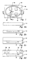
- FIG 1 thereshown is a top view of the inventive device 5.
- the top surface of the device has an oxide covering 70 and four leadouts 50, 52, 54 and 56, which may have contact cuts. These four leadouts serve as connection points to internal circuitry seen in Figures for external circuitry (not shown).
- a substrate 10 is formed out of a semiconductor material, preferably P-type monocrystalline silicon.
- Figure 2b shows a buried layer 30 being diffused into substrate 10, using a dopant to form an N+-type region.
- the buried layer of this chip is shown as extending beneath both leadouts 50 and 52 in Figure 2d, and may also extend under leadouts 54 and 56.
- one buried layer 30 extends under all of the leadouts, it may be used subsequently as an etch stop. However, there may be four separate buried layers, each contacting only a single leadout.
- an epitaxial layer 40 is grown on the upper surface of the buried layer 30 and on substrate 10.
- the epitaxial layer 40 in this embodiment will be of N-type silicon.
- leadouts 50, 52, 54 and 56 as well as isolation region 58 are diffused in epitaxial layer 40 as shown in Figure 2d (only leadouts 50 and 52 are shown).
- the leadouts are diffused so as to contact the buried layer 30.
- the isolation region 58 can be circular as seen in Figure 1 and can surround the other parts of the transducer, but is not required to do so.
- Both the isolation region 58 and leadouts 50, 52, 54 and 56 are formed using the same dopant during the same process step. It is to be noted that the leadouts contact the buried layer 30, and the isolation region 58, which is generally used to isolate circuit elements, contacts the grounded substrate.
- resistor 60 is formed by diffusing a dopant into the epitaxial layer 40.
- the resistor 60 is diffused so that it comes into contact with leadouts 50 and 52.
- a protective overlayer 80 of a conductivity type opposite that of the resistor may be diffused into the resistor 60. It is to be noted that other circuit elements besides a resistor can use the inventive device and method.
- an oxide 70 is formed on the upper surface of the epitaxial layer 40 and N layer 80. Areas over leadouts 50, 52, 54 and 56 can be left uncovered by the oxide to provide optional contact points. This can be seen in Figure 1.
- a diaphragm under the region of the resistor can be formed by etching away a portion of substrate 10.
- Region 20 represents an area of substrate 10 which has been etched away up to buried layer 30.
- An anisotropic etching process may be used to form the diaphragm whereby etching will cease once the etchant reaches the buried layer.
- Figure 3 shows that the structure is the same when viewed along line 2-2 as along line 3-3.
- Figure 4 shows the schematic representation of the circuit of the present embodiment.
- the circuit is a resistive bridge.
Landscapes
- Semiconductor Integrated Circuits (AREA)
- Element Separation (AREA)
- Measuring Fluid Pressure (AREA)
- Pressure Sensors (AREA)
Applications Claiming Priority (2)
| Application Number | Priority Date | Filing Date | Title |
|---|---|---|---|
| US45291589A | 1989-12-18 | 1989-12-18 | |
| US452915 | 1989-12-18 |
Publications (2)
| Publication Number | Publication Date |
|---|---|
| EP0434318A2 true EP0434318A2 (de) | 1991-06-26 |
| EP0434318A3 EP0434318A3 (en) | 1992-08-26 |
Family
ID=23798486
Family Applications (1)
| Application Number | Title | Priority Date | Filing Date |
|---|---|---|---|
| EP19900313684 Withdrawn EP0434318A3 (en) | 1989-12-18 | 1990-12-14 | Low sheet resistance diffused contacts to buried diffused resistors using isolation regions and buried layer |
Country Status (2)
| Country | Link |
|---|---|
| EP (1) | EP0434318A3 (de) |
| JP (1) | JPH03190281A (de) |
Cited By (2)
| Publication number | Priority date | Publication date | Assignee | Title |
|---|---|---|---|---|
| EP0729019A3 (de) * | 1995-02-27 | 1996-12-11 | Motorola Inc | Verfahren zur Herstellung eines piezoresistiven Drucksensors und ein piezoresistiver Drucksensor |
| WO2010046233A1 (de) * | 2008-10-22 | 2010-04-29 | Robert Bosch Gmbh | Verfahren zum erzeugen von monokristallinen piezowiderständen und drucksensorelemente mit solchen piezowiderständen |
Family Cites Families (5)
| Publication number | Priority date | Publication date | Assignee | Title |
|---|---|---|---|---|
| FR1534711A (fr) * | 1966-04-13 | 1968-08-02 | Rca Corp | Résistance et procédé pour sa fabrication |
| EP0054303B1 (de) * | 1980-12-17 | 1986-06-11 | Matsushita Electric Industrial Co., Ltd. | Integrierte Halbleiterschaltung |
| US4742021A (en) * | 1985-05-05 | 1988-05-03 | Burr-Brown Corporation | Subsurface zener diode and method of making |
| DE3850855T2 (de) * | 1987-11-13 | 1994-11-10 | Nissan Motor | Halbleitervorrichtung. |
| EP0437949A1 (de) * | 1989-12-18 | 1991-07-24 | Honeywell Inc. | Doppeldiffundierte Kontaktleitung für Halbleiterbauelement |
-
1990
- 1990-11-19 JP JP2311685A patent/JPH03190281A/ja active Pending
- 1990-12-14 EP EP19900313684 patent/EP0434318A3/en not_active Withdrawn
Cited By (2)
| Publication number | Priority date | Publication date | Assignee | Title |
|---|---|---|---|---|
| EP0729019A3 (de) * | 1995-02-27 | 1996-12-11 | Motorola Inc | Verfahren zur Herstellung eines piezoresistiven Drucksensors und ein piezoresistiver Drucksensor |
| WO2010046233A1 (de) * | 2008-10-22 | 2010-04-29 | Robert Bosch Gmbh | Verfahren zum erzeugen von monokristallinen piezowiderständen und drucksensorelemente mit solchen piezowiderständen |
Also Published As
| Publication number | Publication date |
|---|---|
| JPH03190281A (ja) | 1991-08-20 |
| EP0434318A3 (en) | 1992-08-26 |
Similar Documents
| Publication | Publication Date | Title |
|---|---|---|
| US5719069A (en) | One-chip integrated sensor process | |
| JP2940293B2 (ja) | 半導体加速度センサの製造方法 | |
| JPS59117271A (ja) | 圧力感知素子を有する半導体装置とその製造法 | |
| EP0182032A2 (de) | SoI-Halbleiteranordnung und Verfahren zu ihrer Herstellung | |
| EP0340022A1 (de) | Mechanischer Sensor für Hochtemperaturumgebungen | |
| US6875673B2 (en) | Method of producing semiconductor device | |
| US4945762A (en) | Silicon sensor with trimmable wheatstone bridge | |
| EP0340904B1 (de) | Monolithische druckempfindliche integrierte Schaltung und Verfahren zu deren Herstellung | |
| US4110782A (en) | Monolithic integrated circuit transistor having very low collector resistance | |
| US4977101A (en) | Monolithic pressure sensitive integrated circuit | |
| US4046605A (en) | Method of electrically isolating individual semiconductor circuits in a wafer | |
| EP0434318A2 (de) | Diffundierte Kontakte mit niedriger Schichtwiderstand für vergrabene diffundierte Widerstand unter Verwendung von Isolationszonen und einer vergrabenen Zone | |
| JP3503146B2 (ja) | 半導体装置の製造方法 | |
| JPH0799760B2 (ja) | 半導体装置 | |
| US4740482A (en) | Method of manufacturing bipolar transistor | |
| JPH10135484A (ja) | 半導体装置 | |
| US5360521A (en) | Method for etching silicon | |
| JP2850558B2 (ja) | 半導体圧力センサおよびその製造方法 | |
| EP0150307B1 (de) | Widerstandsstruktur für Transistor mit Basiskontakten aus polykristallinem Silizium | |
| JPH06204408A (ja) | 半導体装置用拡散抵抗 | |
| US5107309A (en) | Double diffused leadout for a semiconductor device | |
| GB1563193A (en) | Semiconductor devices | |
| JPH0311107B2 (de) | ||
| US3918079A (en) | Encapsulated beam lead construction for semiconductor device and assembly and method | |
| JP3179938B2 (ja) | 半導体保護回路 |
Legal Events
| Date | Code | Title | Description |
|---|---|---|---|
| PUAI | Public reference made under article 153(3) epc to a published international application that has entered the european phase |
Free format text: ORIGINAL CODE: 0009012 |
|
| AK | Designated contracting states |
Kind code of ref document: A2 Designated state(s): DE FR IT NL |
|
| PUAL | Search report despatched |
Free format text: ORIGINAL CODE: 0009013 |
|
| AK | Designated contracting states |
Kind code of ref document: A3 Designated state(s): DE FR IT NL |
|
| STAA | Information on the status of an ep patent application or granted ep patent |
Free format text: STATUS: THE APPLICATION HAS BEEN WITHDRAWN |
|
| 18W | Application withdrawn |
Withdrawal date: 19921026 |
|
| R18W | Application withdrawn (corrected) |
Effective date: 19921026 |