EP0433644A2 - A neural net for data-processing - Google Patents
A neural net for data-processing Download PDFInfo
- Publication number
- EP0433644A2 EP0433644A2 EP90121486A EP90121486A EP0433644A2 EP 0433644 A2 EP0433644 A2 EP 0433644A2 EP 90121486 A EP90121486 A EP 90121486A EP 90121486 A EP90121486 A EP 90121486A EP 0433644 A2 EP0433644 A2 EP 0433644A2
- Authority
- EP
- European Patent Office
- Prior art keywords
- neural net
- ecm
- matrix
- net according
- electrode
- Prior art date
- Legal status (The legal status is an assumption and is not a legal conclusion. Google has not performed a legal analysis and makes no representation as to the accuracy of the status listed.)
- Granted
Links
Images

Classifications
-
- G—PHYSICS
- G06—COMPUTING; CALCULATING OR COUNTING
- G06N—COMPUTING ARRANGEMENTS BASED ON SPECIFIC COMPUTATIONAL MODELS
- G06N3/00—Computing arrangements based on biological models
- G06N3/02—Neural networks
- G06N3/06—Physical realisation, i.e. hardware implementation of neural networks, neurons or parts of neurons
- G06N3/063—Physical realisation, i.e. hardware implementation of neural networks, neurons or parts of neurons using electronic means
-
- G—PHYSICS
- G11—INFORMATION STORAGE
- G11C—STATIC STORES
- G11C13/00—Digital stores characterised by the use of storage elements not covered by groups G11C11/00, G11C23/00, or G11C25/00
- G11C13/04—Digital stores characterised by the use of storage elements not covered by groups G11C11/00, G11C23/00, or G11C25/00 using optical elements ; using other beam accessed elements, e.g. electron or ion beam
- G11C13/047—Digital stores characterised by the use of storage elements not covered by groups G11C11/00, G11C23/00, or G11C25/00 using optical elements ; using other beam accessed elements, e.g. electron or ion beam using electro-optical elements
-
- G—PHYSICS
- G11—INFORMATION STORAGE
- G11C—STATIC STORES
- G11C7/00—Arrangements for writing information into, or reading information out from, a digital store
- G11C7/005—Arrangements for writing information into, or reading information out from, a digital store with combined beam-and individual cell access
Landscapes
- Engineering & Computer Science (AREA)
- Physics & Mathematics (AREA)
- Theoretical Computer Science (AREA)
- Health & Medical Sciences (AREA)
- Life Sciences & Earth Sciences (AREA)
- Biomedical Technology (AREA)
- Biophysics (AREA)
- Neurology (AREA)
- Mathematical Physics (AREA)
- Data Mining & Analysis (AREA)
- Evolutionary Computation (AREA)
- General Health & Medical Sciences (AREA)
- Molecular Biology (AREA)
- Computing Systems (AREA)
- General Engineering & Computer Science (AREA)
- General Physics & Mathematics (AREA)
- Computational Linguistics (AREA)
- Software Systems (AREA)
- Artificial Intelligence (AREA)
- Image Processing (AREA)
- Electrochromic Elements, Electrophoresis, Or Variable Reflection Or Absorption Elements (AREA)
- Electrotherapy Devices (AREA)
- Pharmaceuticals Containing Other Organic And Inorganic Compounds (AREA)
- Elevator Control (AREA)
- Exposure Control For Cameras (AREA)
- Peptides Or Proteins (AREA)
Abstract
a plurality of line electrodes (Ri),
a plurality of column electrodes (Cj), and
a plurality of ordered regions (Aij) in which line electrodes (Ri) and column electrodes (Cj) are interconnected. At least some of the connecting regions (Aij) include electrochromic material (ECM).
Description
- The present invention relates to a neural net for data-processing and a method of data-processing which provides for the use of the neural net.
- Interest in neural nets based on neuron models has increased considerably in recent times.
- Many factors have contributed to this: neurobiologists have started to improve their understanding of biological processing mechanisms, the availability of low-cost computational power has enabled detailed analysis of circuit models of biological systems and, finally, interest in parallel processing and analog VLSI (very large-scale integration), which in turn are suitable for embodiment in neuron-type circuits, has increased. These developments have been accompanied by the formulation of new neuron models.
- According to J.J. Hopfield's model (see Proceedings of the National Academy of Science U.S.A., Vol.79, p. 2554, 1982) a neuron can be imitated by an adder element with a non-linear transfer characteristic whose inputs are "weighted" with coefficients characteristic of the net.
- In a known circuit (see C. Mead, "Analog VLSI and Neural Systems", Addison-Wesley, 1989), the characteristic weighting coefficients of the net can be defined by the transconductance values of MOS transistors and these values can be defined in turn by the resistance values of resistors. A neural net is thus defined once the values of the weighting coefficients assigned to its inputs have been defined. A neural net for a new and different function, however, has to be constructed from scratch with transistors having correspondingly different transconductances.
- A neural net which can be adapted to carry out different functions is described in U.S. Patent No. 4,760,437. This known neural net includes a matrix comprising a plurality of line electrodes, a plurality of column electrodes, and a plurality of ordered regions in which line electrodes and column electrodes intersect. An element of photoconductive material is associated with each region of intersection and the electrical resistance of the element is determined by the intensity of light caused to fall thereon. The resistance of the element thus determined corresponds to the value of a weighting coefficient associated with the location in the matrix to which the element belongs.
- A mask, such as a photographic plate, is therefore associated with a neuron matrix of this type, the mask having zones whose transparencies differ in dependence on the weighting coefficients to be assigned to the various locations in the matrix. The matrix is then illuminated through the mask by a uniform-light source and the matrix thus becomes "specialised" to carry out the desired function.
- With a neural net according to the United States patent cited above, the mask by means of which the electrical resistances of the photosensitive elements of the matrix are defined has to be replaced in order to modify the function carried out by the net. Obviously, this kind of operation cannot be carried out continuously during processing. In other words, the neural net according to U.S. Patent No. 4,760,437 does not have a so-called "learning capability", that is, a capacity for the "on-line" alteration or up-dating of the weightings associated with at least some locations in the matrix.
- The object of the present invention is to provide a neural net of the aforesaid type which is formed so as to have a learning capability.
- According to the invention, this object is achieved, by means of a neural data-processing net including active electronic devices associated with a matrix comprising a plurality of line electrodes, a plurality of column electrodes, and a plurality of ordered regions in which line electrodes and column electrodes are interconnected, the neural net being characterised in that at least some of the connecting regions of the matrix include electrochromic material.
- Electrochromic materials are materials which can be coloured reversibly as a result of the passage of an electrical load. Electrochromism is a phenomenon by which a reversible colour-change can be induced in some materials as a result of an electrochemical process. More precisely, electrochromism can be defined as a persistent but reversible electrochemically-induced optical change.
- Electrochromic materials are therefore suitable for forming elements whose transparency can be changed reversibly by the passage of current pulses through the elements in one direction or the other according to whether their transparency is to be increased or reduced. This property of electrochromic materials enables neural nets with learning capabilities to be formed, as will become clearer from the following.
- The invention also concerns a method of data-processing which provides for the use of a neural net of the type defined above.
- Further characteristics and advantages of the invention will become clear from the detailed description which follows with reference to the appended drawings, provided purely by way of non-limiting example, in which:
- Figure 1 is a diagram showing the structure of a neural net matrix according to the invention,
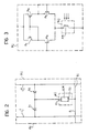
- Figure 2 shows the structure of the circuitry in a region line electrodes and column electrodes of the matrix of Figure 1 are interconnected,
- Figure 3 shows, by way of example, a circuit diagram of a synapse associated with a region in which line electrodes and column electrodes of the matrix are interconnected,
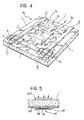
- Figure 4 is a perspective view of a portion of the matrix, and
- Figure 5 is a partial sectional view taken on the line V-V of Figure 4.
- With reference to the drawings, a neural data-processing net according to the invention includes a
support substrate 1 of at least partially transparent material, for example glass. - A matrix structure, generally indicated 2 in Figure 1, is formed on one face of the substrate.
- As will become clearer from the following, the neural net also includes active electronic devices which interact with the
matrix 2 and conveniently are formed on the other face of the supportingsubstrate 1. - In the embodiment to which Figure 1 relates, the
matrix structure 2 comprises a plurality of line electrodes Ri (i = 1, 2 ... n) and a plurality of pairs of column electrodes Ck j (j = 1, 2 ... m, m being equal to or different from n; k = 1,2). - The
matrix 2 of Figure 1 also has a plurality of ordered connecting regions Aij, each of which interconnects a pair of column electrodes and a line electrode. - Figure 2 is a symbolic circuit diagram of a generic connecting region Aij: two diodes, indicated D₁ and D₂, are arranged in series between the column electrodes C¹j and C²j.
- An element, indicated ECM, of electrochromic material, for example, tungsten oxide WO₃, is deposited on a small area of the region Aij, indicated aij. This element has two electrodes E₁, E₂, the first of which is connected to the anode of D₁ and to the cathode of D₂, whilst the second is connected to the line electrode Ri.
- The arrangement of the diodes D₁ and D₂ is such that an electric current can flow through ECM in one direction or the other. Thus, if the column electrodes C¹j and C²j are connected to the positive pole of a direct-current voltage supply and the line electrode Ri is connected to the negative pole (or to earth), a current flows through C²j, D₂, ECM, and the line electrode Ri.
- If the column electrodes are connected to the negative pole of the supply and the line electrode Ri is connected to the positive pole, however, a current will flow through Ri, ECM, D₁ and C¹j, passing through ECM in the opposite direction from that described above.
- As a result of the known properties of electrochromic materials (in this connection see, for example, the article "Electrochromism and Electrochromic Devices" by B. Scrosate, Chimicaoggi, June 1989, pp. 41-45) a pulse of current through ECM in one direction or the other has the effect of increasing or reducing (persistently but reversibly) the transparency of the electrochromic element.
- Synaptic circuits are formed on the other face of the
support substrate 1 in regions Bij (Figure 3) situated in positions corresponding to the connecting regions Aij of thematrix 2, for example, according to the layout shown in Figure 3. This layout provides for an analog differential amplifier comprising, in known manner, a pair of p-type MOS transistors, indicated M₁ and M₂, and a pair of n-type MOS transistors, indicated M₃ and M₄. The "drains" of M₁ and M₂ are intended to be connected to the positive terminal of a direct-current voltage supply. The "gates" of these transistors are connected to each other and to the "drain" of M₃. - The "sources" of M₁ and M₂ are connected to the "drains" of M₃ and M₄ respectively. The "sources" of M₃ and M₄ are connected to the "drain" of a MOS phototransistor, indicated FM, which, conveniently, is formed in a small area bij facing (through the support substrate 1) the area aij on which the element ECM of electrochromic material is formed. The arrangement is such that light can fall on FM only through ECM and the
support substrate 1. As a result, the intensity of the light falling on FM depends on the transparency of the associated ECM which, moreover, can be modified and, in particular, can be reduced or increased by the passage of current pulses through ECM in one direction or the other, as described above. - The weighting coefficient associated with FM can therefore be modified "on line" so that the neural net as a whole has a learning capacity.
- Figures 4 and 5 are qualitative illustrations of an embodiment of an individual connecting cell or region Aij of the
matrix 2. - Conveniently, the column electrodes are made of metal, for example, gold, aluminium, tungsten, molybdenum, niobium, nickel (or even other metals) or alloys thereof. A line electrode Ri with which the electrode E₂ of the electrochromic element ECM is formed integrally, is deposited on the column electrodes after the interposition of layers F of an insulating material constituted, for example, by SiO₂.
- The electrode E₁ of the element ECM is formed in two parts:
a first part, indicated E′₁, formed by a mixture including a solid-state polymeric electrolyte, such as a polyethylene oxide, and an alkali metal salt, for example, LiC₁O₄ or LiCF₃SO₃, and
a second part, indicated E˝₁, constituted by an alkali metal such as lithium or sodium. - Still with reference to Figure 4, the diodes D₁ and D₂ are formed by two p-n junctions, for example of silicon.
- As can be seen from Figure 5, the phototransistor FM of a synaptic circuit is formed on the lower face of the
transparent support 1 in correspondence with the associated electrochromic element ECM. The phototransistor is formed, in known manner, by the deposition of a layer ofamorphous silicon 100 suitably doped to form the drain, source and gate regions. The gate, drain and source terminals are indicated 101, 102 and 103 in Figure 5. - Naturally, the principle of the invention remaining the same, the forms of embodiment and details of construction may be varied widely with respect to those described and illustrated purely by way of non-limiting example, without thereby departing from the scope of the present invention.
- The foregoing description describes, with reference to the appended drawings, an embodiment in which the
matrix 2 includes a plurality of pairs of column electrodes. As has been seen, this embodiment enables the transparency of individual electrochromic elements to be increased and reduced selectively in order to give the neural net a learning capability. - For applications in which there is expected to be a need or opportunity for the neural net to have a learning capacity such that, in operation, the transparency of the elements ECM always has to be modified in the same way, that is, always to increase their transparency or always to reduce their transparency, the matrix could be formed with single column electrodes and without the need for one-way conductive elements.
- Finally, the definition of lines and columns in the foregoing description is of course purely conventional and does not presuppose the parallelism of the line electrodes or of the column electrodes or necesarily imply that the column electrodes are perpendicular to the line electrodes.
Claims (17)
a first electrode (E₁) connected to each column electrode of a pair of column electrodes (C¹j, C²j) by first and second one-way conductive elements (D₁, D₂) respectively, and
a second electrode (E₂) connected to a line electrode (Ri);
the one-way conductive elements (D₁, D₂) being adapted to enable a current to flow in the electrochromic element (ECM) selectively from the first electrode (E₁) of the electrochromic element to the second (E₂) or from the second electrode (E₂) to the first (E₁).
a first portion (E′₁) arranged in contact with the metal-oxide layer and constituted by a complex including a solid-state polymeric electrolyte and an alkali metal salt, and
a second portion (E˝₁) connected to the column electrodes and including an alkali metal.
entering the data in a neural net including a matrix (2) comprising a plurality of line electrodes (Ri), a plurality of column electrodes (Cj), and a plurality of ordered regions (Aij) in which line electrodes (Ri) and column electrodes (Cj) are interconnected,
characterised in that at least some of the connecting regions (Aij) include electrochromic material (ECM; and in that the processing of the data is affected by light which is made to fall on the electrochromic portion (ECM) of at least one of the connecting regions (Aij) of the matrix (2).
Applications Claiming Priority (2)
| Application Number | Priority Date | Filing Date | Title |
|---|---|---|---|
| IT6800689 | 1989-11-15 | ||
| IT06800689A IT1237269B (en) | 1989-11-15 | 1989-11-15 | NEURAL NETWORK WITH LEARNING SKILLS FOR THE PROCESSING OF INFORMATION, AND PROCEDURE FOR THE TREATMENT OF INFORMATION WITH THE USE OF SUCH NETWORK. |
Publications (3)
| Publication Number | Publication Date |
|---|---|
| EP0433644A2 true EP0433644A2 (en) | 1991-06-26 |
| EP0433644A3 EP0433644A3 (en) | 1992-02-26 |
| EP0433644B1 EP0433644B1 (en) | 1995-10-04 |
Family
ID=11307139
Family Applications (1)
| Application Number | Title | Priority Date | Filing Date |
|---|---|---|---|
| EP90121486A Expired - Lifetime EP0433644B1 (en) | 1989-11-15 | 1990-11-09 | A neural net for data-processing |
Country Status (5)
| Country | Link |
|---|---|
| US (1) | US5204937A (en) |
| EP (1) | EP0433644B1 (en) |
| AT (1) | ATE128779T1 (en) |
| DE (1) | DE69022828T2 (en) |
| IT (1) | IT1237269B (en) |
Cited By (1)
| Publication number | Priority date | Publication date | Assignee | Title |
|---|---|---|---|---|
| GB2316970A (en) * | 1996-09-05 | 1998-03-11 | Kenneth Scaddan | Threshold water excluding device which rises as a door closes |
Families Citing this family (7)
| Publication number | Priority date | Publication date | Assignee | Title |
|---|---|---|---|---|
| US6507828B1 (en) * | 1998-06-19 | 2003-01-14 | Jason Leonard | Neuron circuit and related techniques |
| US6763340B1 (en) * | 2000-09-22 | 2004-07-13 | The United States Of America As Represented By The Secretary Of The Air Force | Microelectromechanical system artificial neural network device |
| WO2002071139A1 (en) * | 2001-03-07 | 2002-09-12 | Acreo Ab | Electrochemical pixel device |
| EP2015135B1 (en) * | 2002-03-07 | 2012-02-01 | Acreo AB | Electrochemical device |
| US7829162B2 (en) * | 2006-08-29 | 2010-11-09 | international imagining materials, inc | Thermal transfer ribbon |
| US10139693B2 (en) | 2015-06-19 | 2018-11-27 | International Business Machines Corporation | Synaptic electronic devices with electrochromic device |
| CN113504683A (en) * | 2021-07-23 | 2021-10-15 | 中国科学技术大学 | Preparation method of electrochromic device and method for simulating human brain neuron transmission information |
Citations (4)
| Publication number | Priority date | Publication date | Assignee | Title |
|---|---|---|---|---|
| EP0127140A2 (en) * | 1983-05-25 | 1984-12-05 | Hitachi, Ltd. | Information holding device |
| US4498156A (en) * | 1981-09-24 | 1985-02-05 | Rockwell International Corporation | Electrochromic nonvolatile memory device |
| WO1986001931A1 (en) * | 1984-09-07 | 1986-03-27 | Pa Consulting Services Limited | Method and apparatus for loading information into an integrated circuit semiconductor device |
| US4760437A (en) * | 1986-01-03 | 1988-07-26 | American Telephone And Telegraph Company, At&T Bell Laboratories | Neural networks |
Family Cites Families (12)
| Publication number | Priority date | Publication date | Assignee | Title |
|---|---|---|---|---|
| SU529467A1 (en) * | 1975-07-21 | 1976-09-25 | Физико-Технический Институт Им. С.В.Стародубцева Ан Узбекской Сср | Electron-optical correlator |
| JPS5335565A (en) * | 1976-09-14 | 1978-04-03 | Sharp Corp | Electrochromic display device |
| US4335938A (en) * | 1979-08-30 | 1982-06-22 | American Cyanamid Company | Electrochromic cells with improved electrolyte system |
| US4392209A (en) * | 1981-03-31 | 1983-07-05 | Ibm Corporation | Randomly accessible memory display |
| NL8103377A (en) * | 1981-07-16 | 1983-02-16 | Philips Nv | DISPLAY DEVICE. |
| US4488781A (en) * | 1982-01-25 | 1984-12-18 | American Cyanamid Company | Method for manufacturing an electrochromic display device and device produced thereby |
| AU2485788A (en) * | 1987-07-28 | 1989-03-01 | Maxdem, Inc. | Electrically settable resistance device |
| US4931763A (en) * | 1988-02-16 | 1990-06-05 | California Institute Of Technology | Memory switches based on metal oxide thin films |
| US4943556A (en) * | 1988-09-30 | 1990-07-24 | The United States Of America As Represented By The Secretary Of The Navy | Superconducting neural network computer and sensor array |
| US4916470A (en) * | 1988-11-16 | 1990-04-10 | Xerox Corporation | Image bar with electrochromic switching system |
| US5010512A (en) * | 1989-01-12 | 1991-04-23 | International Business Machines Corp. | Neural network having an associative memory that learns by example |
| US4969021A (en) * | 1989-06-12 | 1990-11-06 | California Institute Of Technology | Porous floating gate vertical mosfet device with programmable analog memory |
-
1989
- 1989-11-15 IT IT06800689A patent/IT1237269B/en active IP Right Grant
-
1990
- 1990-11-09 EP EP90121486A patent/EP0433644B1/en not_active Expired - Lifetime
- 1990-11-09 DE DE69022828T patent/DE69022828T2/en not_active Expired - Fee Related
- 1990-11-09 AT AT90121486T patent/ATE128779T1/en active
- 1990-11-09 US US07/612,233 patent/US5204937A/en not_active Expired - Fee Related
Patent Citations (4)
| Publication number | Priority date | Publication date | Assignee | Title |
|---|---|---|---|---|
| US4498156A (en) * | 1981-09-24 | 1985-02-05 | Rockwell International Corporation | Electrochromic nonvolatile memory device |
| EP0127140A2 (en) * | 1983-05-25 | 1984-12-05 | Hitachi, Ltd. | Information holding device |
| WO1986001931A1 (en) * | 1984-09-07 | 1986-03-27 | Pa Consulting Services Limited | Method and apparatus for loading information into an integrated circuit semiconductor device |
| US4760437A (en) * | 1986-01-03 | 1988-07-26 | American Telephone And Telegraph Company, At&T Bell Laboratories | Neural networks |
Cited By (1)
| Publication number | Priority date | Publication date | Assignee | Title |
|---|---|---|---|---|
| GB2316970A (en) * | 1996-09-05 | 1998-03-11 | Kenneth Scaddan | Threshold water excluding device which rises as a door closes |
Also Published As
| Publication number | Publication date |
|---|---|
| ATE128779T1 (en) | 1995-10-15 |
| IT1237269B (en) | 1993-05-27 |
| US5204937A (en) | 1993-04-20 |
| IT8968006A0 (en) | 1989-11-15 |
| EP0433644A3 (en) | 1992-02-26 |
| DE69022828D1 (en) | 1995-11-09 |
| EP0433644B1 (en) | 1995-10-04 |
| DE69022828T2 (en) | 1996-03-14 |
Similar Documents
| Publication | Publication Date | Title |
|---|---|---|
| EP0377908B1 (en) | Neural network having an associative memory that learns by example | |
| DE112018005726B4 (en) | COUNTER-BASED RESISTIVE PROCESSING UNIT FOR PROGRAMMABLE AND RECONFIGURABLE ARTIFICIAL NEURAL NETWORKS | |
| Khalid | Review on various memristor models, characteristics, potential applications, and future works | |
| Merrikh-Bayat et al. | Memristor crossbar-based hardware implementation of the IDS method | |
| US5296835A (en) | Variable resistor and neuro device using the variable resistor for weighting | |
| EP0433644B1 (en) | A neural net for data-processing | |
| WO1990004836A1 (en) | Artificial neural network implementation | |
| Pisarev et al. | 3D memory matrix based on a composite memristor-diode crossbar for a neuromorphic processor | |
| Gacem et al. | Neuromorphic function learning with carbon nanotube based synapses | |
| Foo et al. | Analog components for the VLSI of neural networks | |
| Hjelmfelt et al. | Implementation of logic functions and computations by chemical kinetics | |
| KR20200058196A (en) | Batch normalization apparatus based on resistive memory for binary neural network | |
| US20230186060A1 (en) | Novel neuromorphic vision system | |
| US5305250A (en) | Analog continuous-time MOS vector multiplier circuit and a programmable MOS realization for feedback neural networks | |
| US6548316B1 (en) | Monolithic semiconductor device and method of manufacturing the same | |
| EP0411761B1 (en) | Neuronal processing element | |
| US5220202A (en) | Memory device and memory apparatus using the same suitable for neural network | |
| KR20210157049A (en) | Neural network using weighted synapse based on resistive random access memory array | |
| Perez et al. | Neuromorphic-based Boolean and reversible logic circuits from organic electrochemical transistors | |
| Huang et al. | Adaptive SRM neuron based on NbOx memristive device for neuromorphic computing | |
| KR0183406B1 (en) | Capacitive structures for weighted summation, as used in neural nets | |
| US5212377A (en) | Thin-film neuron network with optical programming | |
| Harada et al. | A time-domain analog weighted-sum calculation circuit using ferroelectric-gate field-effect transistors for artificial intelligence processors | |
| JP2926737B2 (en) | Optical information processing device | |
| Gupta et al. | Artificial Neural Network Hardware Implementation: Recent Trends and Applications |
Legal Events
| Date | Code | Title | Description |
|---|---|---|---|
| PUAI | Public reference made under article 153(3) epc to a published international application that has entered the european phase |
Free format text: ORIGINAL CODE: 0009012 |
|
| AK | Designated contracting states |
Kind code of ref document: A2 Designated state(s): AT BE CH DE DK ES FR GB GR LI LU NL SE |
|
| PUAL | Search report despatched |
Free format text: ORIGINAL CODE: 0009013 |
|
| AK | Designated contracting states |
Kind code of ref document: A3 Designated state(s): AT BE CH DE DK ES FR GB GR LI LU NL SE |
|
| 17P | Request for examination filed |
Effective date: 19920314 |
|
| 17Q | First examination report despatched |
Effective date: 19940503 |
|
| GRAA | (expected) grant |
Free format text: ORIGINAL CODE: 0009210 |
|
| AK | Designated contracting states |
Kind code of ref document: B1 Designated state(s): AT BE CH DE DK ES FR GB GR LI LU NL SE |
|
| PG25 | Lapsed in a contracting state [announced via postgrant information from national office to epo] |
Ref country code: GR Free format text: LAPSE BECAUSE OF FAILURE TO SUBMIT A TRANSLATION OF THE DESCRIPTION OR TO PAY THE FEE WITHIN THE PRESCRIBED TIME-LIMIT Effective date: 19951004 Ref country code: ES Free format text: THE PATENT HAS BEEN ANNULLED BY A DECISION OF A NATIONAL AUTHORITY Effective date: 19951004 Ref country code: DK Effective date: 19951004 Ref country code: AT Effective date: 19951004 |
|
| REF | Corresponds to: |
Ref document number: 128779 Country of ref document: AT Date of ref document: 19951015 Kind code of ref document: T |
|
| ET | Fr: translation filed | ||
| REF | Corresponds to: |
Ref document number: 69022828 Country of ref document: DE Date of ref document: 19951109 |
|
| PG25 | Lapsed in a contracting state [announced via postgrant information from national office to epo] |
Ref country code: LU Free format text: LAPSE BECAUSE OF NON-PAYMENT OF DUE FEES Effective date: 19951130 |
|
| PGFP | Annual fee paid to national office [announced via postgrant information from national office to epo] |
Ref country code: CH Payment date: 19951130 Year of fee payment: 6 |
|
| PG25 | Lapsed in a contracting state [announced via postgrant information from national office to epo] |
Ref country code: SE Effective date: 19960104 |
|
| REG | Reference to a national code |
Ref country code: CH Ref legal event code: PL |
|
| PLBE | No opposition filed within time limit |
Free format text: ORIGINAL CODE: 0009261 |
|
| STAA | Information on the status of an ep patent application or granted ep patent |
Free format text: STATUS: NO OPPOSITION FILED WITHIN TIME LIMIT |
|
| 26N | No opposition filed | ||
| PG25 | Lapsed in a contracting state [announced via postgrant information from national office to epo] |
Ref country code: LI Free format text: LAPSE BECAUSE OF FAILURE TO SUBMIT A TRANSLATION OF THE DESCRIPTION OR TO PAY THE FEE WITHIN THE PRESCRIBED TIME-LIMIT Effective date: 19961130 Ref country code: CH Free format text: LAPSE BECAUSE OF FAILURE TO SUBMIT A TRANSLATION OF THE DESCRIPTION OR TO PAY THE FEE WITHIN THE PRESCRIBED TIME-LIMIT Effective date: 19961130 |
|
| PGFP | Annual fee paid to national office [announced via postgrant information from national office to epo] |
Ref country code: DE Payment date: 20001030 Year of fee payment: 11 |
|
| PGFP | Annual fee paid to national office [announced via postgrant information from national office to epo] |
Ref country code: GB Payment date: 20001108 Year of fee payment: 11 |
|
| PGFP | Annual fee paid to national office [announced via postgrant information from national office to epo] |
Ref country code: FR Payment date: 20001110 Year of fee payment: 11 |
|
| PGFP | Annual fee paid to national office [announced via postgrant information from national office to epo] |
Ref country code: NL Payment date: 20001130 Year of fee payment: 11 |
|
| PGFP | Annual fee paid to national office [announced via postgrant information from national office to epo] |
Ref country code: BE Payment date: 20010123 Year of fee payment: 11 |
|
| PG25 | Lapsed in a contracting state [announced via postgrant information from national office to epo] |
Ref country code: GB Free format text: LAPSE BECAUSE OF NON-PAYMENT OF DUE FEES Effective date: 20011109 |
|
| PG25 | Lapsed in a contracting state [announced via postgrant information from national office to epo] |
Ref country code: BE Free format text: LAPSE BECAUSE OF NON-PAYMENT OF DUE FEES Effective date: 20011130 |
|
| REG | Reference to a national code |
Ref country code: GB Ref legal event code: IF02 |
|
| BERE | Be: lapsed |
Owner name: ENIRICERCHE S.P.A. Effective date: 20011130 |
|
| PG25 | Lapsed in a contracting state [announced via postgrant information from national office to epo] |
Ref country code: NL Free format text: LAPSE BECAUSE OF NON-PAYMENT OF DUE FEES Effective date: 20020601 |
|
| GBPC | Gb: european patent ceased through non-payment of renewal fee |
Effective date: 20011109 |
|
| PG25 | Lapsed in a contracting state [announced via postgrant information from national office to epo] |
Ref country code: DE Free format text: LAPSE BECAUSE OF NON-PAYMENT OF DUE FEES Effective date: 20020702 |
|
| PG25 | Lapsed in a contracting state [announced via postgrant information from national office to epo] |
Ref country code: FR Free format text: LAPSE BECAUSE OF NON-PAYMENT OF DUE FEES Effective date: 20020730 |
|
| NLV4 | Nl: lapsed or anulled due to non-payment of the annual fee |
Effective date: 20020601 |
|
| REG | Reference to a national code |
Ref country code: FR Ref legal event code: ST |
|
| REG | Reference to a national code |
Ref country code: FR Ref legal event code: ST |