EP0429979A2 - Abstimmen des Bandabstands einer halbleitenden Quantumwell-Struktur - Google Patents
Abstimmen des Bandabstands einer halbleitenden Quantumwell-Struktur Download PDFInfo
- Publication number
- EP0429979A2 EP0429979A2 EP90121911A EP90121911A EP0429979A2 EP 0429979 A2 EP0429979 A2 EP 0429979A2 EP 90121911 A EP90121911 A EP 90121911A EP 90121911 A EP90121911 A EP 90121911A EP 0429979 A2 EP0429979 A2 EP 0429979A2
- Authority
- EP
- European Patent Office
- Prior art keywords
- quantum well
- well structure
- heterostructure
- tuning
- forming
- Prior art date
- Legal status (The legal status is an assumption and is not a legal conclusion. Google has not performed a legal analysis and makes no representation as to the accuracy of the status listed.)
- Withdrawn
Links
Images


Classifications
-
- B—PERFORMING OPERATIONS; TRANSPORTING
- B82—NANOTECHNOLOGY
- B82Y—SPECIFIC USES OR APPLICATIONS OF NANOSTRUCTURES; MEASUREMENT OR ANALYSIS OF NANOSTRUCTURES; MANUFACTURE OR TREATMENT OF NANOSTRUCTURES
- B82Y20/00—Nanooptics, e.g. quantum optics or photonic crystals
-
- H—ELECTRICITY
- H01—ELECTRIC ELEMENTS
- H01S—DEVICES USING THE PROCESS OF LIGHT AMPLIFICATION BY STIMULATED EMISSION OF RADIATION [LASER] TO AMPLIFY OR GENERATE LIGHT; DEVICES USING STIMULATED EMISSION OF ELECTROMAGNETIC RADIATION IN WAVE RANGES OTHER THAN OPTICAL
- H01S5/00—Semiconductor lasers
- H01S5/30—Structure or shape of the active region; Materials used for the active region
- H01S5/34—Structure or shape of the active region; Materials used for the active region comprising quantum well or superlattice structures, e.g. single quantum well [SQW] lasers, multiple quantum well [MQW] lasers or graded index separate confinement heterostructure [GRINSCH] lasers
-
- H—ELECTRICITY
- H10—SEMICONDUCTOR DEVICES; ELECTRIC SOLID-STATE DEVICES NOT OTHERWISE PROVIDED FOR
- H10P—GENERIC PROCESSES OR APPARATUS FOR THE MANUFACTURE OR TREATMENT OF DEVICES COVERED BY CLASS H10
- H10P14/00—Formation of materials, e.g. in the shape of layers or pillars
- H10P14/20—Formation of materials, e.g. in the shape of layers or pillars of semiconductor materials
- H10P14/38—Formation of materials, e.g. in the shape of layers or pillars of semiconductor materials characterised by treatments done after the formation of the materials
- H10P14/3824—Intermixing, interdiffusion or disordering of III-V heterostructures, e.g. IILD
-
- H—ELECTRICITY
- H10—SEMICONDUCTOR DEVICES; ELECTRIC SOLID-STATE DEVICES NOT OTHERWISE PROVIDED FOR
- H10P—GENERIC PROCESSES OR APPARATUS FOR THE MANUFACTURE OR TREATMENT OF DEVICES COVERED BY CLASS H10
- H10P95/00—Generic processes or apparatus for manufacture or treatments not covered by the other groups of this subclass
- H10P95/90—Thermal treatments, e.g. annealing or sintering
- H10P95/904—Thermal treatments, e.g. annealing or sintering of Group III-V semiconductors
-
- H—ELECTRICITY
- H01—ELECTRIC ELEMENTS
- H01S—DEVICES USING THE PROCESS OF LIGHT AMPLIFICATION BY STIMULATED EMISSION OF RADIATION [LASER] TO AMPLIFY OR GENERATE LIGHT; DEVICES USING STIMULATED EMISSION OF ELECTROMAGNETIC RADIATION IN WAVE RANGES OTHER THAN OPTICAL
- H01S5/00—Semiconductor lasers
- H01S5/20—Structure or shape of the semiconductor body to guide the optical wave ; Confining structures perpendicular to the optical axis, e.g. index or gain guiding, stripe geometry, broad area lasers, gain tailoring, transverse or lateral reflectors, special cladding structures, MQW barrier reflection layers
- H01S5/2054—Methods of obtaining the confinement
- H01S5/2059—Methods of obtaining the confinement by means of particular conductivity zones, e.g. obtained by particle bombardment or diffusion
- H01S5/2063—Methods of obtaining the confinement by means of particular conductivity zones, e.g. obtained by particle bombardment or diffusion obtained by particle bombardment
-
- H—ELECTRICITY
- H01—ELECTRIC ELEMENTS
- H01S—DEVICES USING THE PROCESS OF LIGHT AMPLIFICATION BY STIMULATED EMISSION OF RADIATION [LASER] TO AMPLIFY OR GENERATE LIGHT; DEVICES USING STIMULATED EMISSION OF ELECTROMAGNETIC RADIATION IN WAVE RANGES OTHER THAN OPTICAL
- H01S5/00—Semiconductor lasers
- H01S5/30—Structure or shape of the active region; Materials used for the active region
- H01S5/34—Structure or shape of the active region; Materials used for the active region comprising quantum well or superlattice structures, e.g. single quantum well [SQW] lasers, multiple quantum well [MQW] lasers or graded index separate confinement heterostructure [GRINSCH] lasers
- H01S5/3413—Structure or shape of the active region; Materials used for the active region comprising quantum well or superlattice structures, e.g. single quantum well [SQW] lasers, multiple quantum well [MQW] lasers or graded index separate confinement heterostructure [GRINSCH] lasers comprising partially disordered wells or barriers
-
- H—ELECTRICITY
- H01—ELECTRIC ELEMENTS
- H01S—DEVICES USING THE PROCESS OF LIGHT AMPLIFICATION BY STIMULATED EMISSION OF RADIATION [LASER] TO AMPLIFY OR GENERATE LIGHT; DEVICES USING STIMULATED EMISSION OF ELECTROMAGNETIC RADIATION IN WAVE RANGES OTHER THAN OPTICAL
- H01S5/00—Semiconductor lasers
- H01S5/30—Structure or shape of the active region; Materials used for the active region
- H01S5/34—Structure or shape of the active region; Materials used for the active region comprising quantum well or superlattice structures, e.g. single quantum well [SQW] lasers, multiple quantum well [MQW] lasers or graded index separate confinement heterostructure [GRINSCH] lasers
- H01S5/343—Structure or shape of the active region; Materials used for the active region comprising quantum well or superlattice structures, e.g. single quantum well [SQW] lasers, multiple quantum well [MQW] lasers or graded index separate confinement heterostructure [GRINSCH] lasers in AIIIBV compounds, e.g. AlGaAs-laser, InP-based laser
- H01S5/34313—Structure or shape of the active region; Materials used for the active region comprising quantum well or superlattice structures, e.g. single quantum well [SQW] lasers, multiple quantum well [MQW] lasers or graded index separate confinement heterostructure [GRINSCH] lasers in AIIIBV compounds, e.g. AlGaAs-laser, InP-based laser with a well layer having only As as V-compound, e.g. AlGaAs, InGaAs
- H01S5/3432—Structure or shape of the active region; Materials used for the active region comprising quantum well or superlattice structures, e.g. single quantum well [SQW] lasers, multiple quantum well [MQW] lasers or graded index separate confinement heterostructure [GRINSCH] lasers in AIIIBV compounds, e.g. AlGaAs-laser, InP-based laser with a well layer having only As as V-compound, e.g. AlGaAs, InGaAs the whole junction comprising only (AI)GaAs
Definitions
- This invention pertains to semiconductor heterostructures and, more specifically, to a method of bandgap tuning of a quantum well structure.
- Optical and electrical properties of quantum well structures are of great importance for novel semiconductor device applications.
- the ultimate goal of monolithic integration of optical, optoelectronic and electronic components requires the capability for controllable lateral and vertical modifications of optical constants and electrical characteristics in such components.
- the selective intermixing of group III atoms across heterostructure interfaces, especially in GaAs/AlGaAs quantum well structures, has been extensively studied due to the controllable changes in optical bandgap which accompany well-barrier interdiffusion.
- Impurity-induced compositional disordering is a well known technique for enhancing interdiffusion. It has been successfully applied to the fabrication of superlattice and quantum well heterostructure devices. In particular, IICD has been demonstrated in a variety of structures by using a diffusion process, and also by using ion implantation followed by thermal annealing. Experimental results have shown that ion implantation is a suitable technique for introducing many kinds of impurities into quantum well structures to enhance interdiffusion.
- the range profile of relevance to intermixing is always considered to be the range for energy losses to nuclear damage processes, and the enhancement of interdiffusion is always associated with the presence of implantation induced defects and/or impurities.
- the mass and energy of the implanted ions are always chosen such that the impurities/damage distribution are spatially peaked in the region of interest for intermixing, such as the middle of a multiple quantum well or a superlattice structure.
- Holonyak in U.S. Patent 4,511,408 discloses a method for disordering the layers in a III-V heterostructure by implanting ions directly into the sample (region of intermixing) and then subjecting the sample to thermal annealing. As noted in column 4, lines 30-34, the implantation causes considerable crystal damage in the structure, which in this case was a superlattice.
- the above method for enhancing interdiffusion at heterointerfaces is also disclosed by Hirayama et al. in "Ion-Species Dependence of Interdiffusion in Ion-Implanted GaAs-AlAs Superlattices" , Japanese Journal of Applied Physics, 24, pp. 1498-1502 (1985), and by Cibert et al. in "Kinetics of Implantation Enhanced Interdiffusion of Ga and Al at GaAs-Ga x Al 1-x As Interfaces", Applied Physics Letters, 49(4), pp. 223-225 (1986).
- Hirayama et al. implanted a group of samples containing superlattices with a variety of ion species and then measured the photoluminescence peak shifts while the samples were being annealed. As in Holonyak, the ions were implanted directly into the superlattice structure, causing crystal damage in the region of intermixing which required thermal treatment to effect recovery.
- Hirayama et al. observed that the spectral width of the superlattice structure increased after annealing, and explained that the increase is partly due to the inhomogeneity of the interdiffusion resulting from the inhomogeneous depth profile of implanted impurity density. Cibert et al.
- a method of selectively tuning the bandedge in a quantum well heterostructure includes implanting ions into said heterostructure to form a disordered region near the upper surface of the sample.
- the vacancies and defects created by said implantation step are spatially separated from the quantum well active region.
- the heterostructure is then thermally annealed so that the vacancies diffuse through the active region (quantum wells) and enhance interdiffusion at the heterojunctions, thereby modifying the optical bandgap of the quantum well layers.
- the bandgap tuning is selective because the implantation step can be appropriately controlled.
- the above tuning method can also be used to perform spatially selective bandgap tuning while simultaneously providing laterally isolated conducting areas.
- the heterostructure is masked in accordance with a specified pattern so that unmasked portions correspond to designated regions of said structure where bandgap tuning/appreciable conductivity is desirable.
- the patterned structure is ion implanted and thermally annealed as described above whereby the unmasked regions are tuned. When the ions are electrically active, enhanced interdiffusion and activation of ions occur simultaneously during annealing.
- the novel tuning method can be implemented to fabricate a bandgap tunable semiconductor heterostructure where the active region consists of a quantum well structure such as a single quantum well (SQW), a multiple quantum well (a number of isolated SQWs), or a superlattice (a number of coupled SQWs).
- a quantum well structure such as a single quantum well (SQW), a multiple quantum well (a number of isolated SQWs), or a superlattice (a number of coupled SQWs).
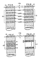
- Figures 1A and 1B are lateral views of exemplary heterostructure devices which were tuned in accordance with the present invention and which include a multiplicity of quantum well layers grown in standard and reverse order, respectively;
- Figure 1C is a lateral view of a double heterostructure semiconductor waveguide where the bandgap of the single quantum well layer was tuned in accordance with the present invention
- Figure 1D is a lateral view of a multiple quantum well (MQW) waveguide where the bandgap of each quantum well layer and subsequently the waveguide as a whole were tuned in accordance with the present invention
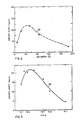
- FIG. 1A graphically illustrates the dependence of photoluminescence (PL) energy shifts on quantum well width for the structure in Figure 1A;
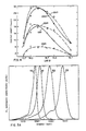
- FIG. 3 graphically illustrates the functional relationship between energy shift and implant fluence for the structure in Figure 1C;
- Figure 4 is a graph of the energy shift versus fluence level for each of the single quantum well layers in Figure 1A;
- Figure 5A is a graph which plots photoluminescence intensity and energy position at low temperature for an unimplanted multiple quantum well structure and for the MQW structure in Figure 1D with implantation at three different fluence levels;
- Figure 6A shows the energy shift versus annealing time (in increments of 15s) for each of the single quantum well layers in the heterostructure of Figure 1A;
- Figure 6B plots energy shift versus annealing time for each of the single quantum well layers in a heterostructure similar to that in Figure 1A but without the ion implantation step.
- the present application discloses a novel method for bandedge tuning in III-V semiconductor material systems by controlling the level of atomic interdiffusion at heterointerfaces of the system.
- the material systems of interest are semiconductor heterostructures having a quantum well structure as an active or part of an active region, and include such devices as a laser, detector, amplifier, modulator waveguide, etc.
- a heterostructure to be tuned is first implanted with low energy ions and then subjected to thermal annealing.
- the implantation creates a disordered region near the upper surface of the heterostructure wherein the vacancies and defects are spatially separated from the quantum well region, thus ensuring that no damage will occur to the active region.
- the heterostructure is thermally annealed so that the vacancies diffuse into the quantum well structure and enhance the intermixing between atoms at the heterointerfaces.
- the samples in Figures 1A-1D were grown by molecular beam epitaxy in a RIBER 2300 system, and include a quantum well active region with alternating layers of a GaAs host material and an AlGaAs barrier material. Although a GaAs/AlGaAs system was investigated, it should be well known to those skilled in the art that other quantum well structures having different compounds would be capable of being tuned in accordance with the present invention. Ion beam implantation was performed using 35 keV 75As + ions having a fluence range of between 5 x 1013 cm ⁇ 2 and .
- the samples were masked prior to implantation so that only half of each piece was implanted, allowing a direct comparison between the respective bandgap changes in the implanted and unimplanted areas.
- rapid thermal annealing RTA was performed at 950°C using the enhanced overpressure proximity technique described by Armiento et al. in Appl. Phys. Lett., Vol. 48, p. 1623 (1986).
- the samples were then mounted strain-free in a cryostat and cooled to 5K. Photoluminescence (PL) and photoluminescence excitation (PLE) spectroscopies were used to monitor the excitonic energies. Room temperature transmission measurements were done on the MQW samples.
- the heterostructures in Figures 1A and 1B consist of a quantum well active region 12 having a series of single quantum well layers labeled SQW1-SQW5 grown in standard and reverse order, respectively.
- the well layers are uncoupled and of varying widths, with the layer SQW1 in each active region being located approximately 300nm below the upper surface 10.
- a barrier layer separates adjacent quantum well layers from one another.
- the barrier material was AlGaAs and the well layers were GaAs .
- surface 10 is implanted with a low energy ion beam to create a disordered region 11 of depth R p (penetration depth of ions).
- the region 11 is spatially separated from the nearest quantum well layer SQW1, thereby preventing the defects created by ion implantation from damaging the active region 12. Consequently, the material quality of the well layers is preserved.
- thermal annealing is performed to enhance the interdiffusion at the well-barrier heterojunctions.
- the structure in Figure 1C is a simple double heterostructure waveguide 13 with a 4nm-wide control single quantum well layer 16 in the middle of 1.2 ⁇ of GaAs .
- Figure ID shows a multiple quantum well waveguide 17 consisting of twenty-five periods of 8nm GaAs single quantum well layers 18 separated by 8nm of Al0.3Ga0.7As barriers 19.
- the upper surface 10 in each of Figures 1C and 1D was ion implanted to create a disordered region 11 of depth Rp.
- the disordered region 11 in both Figures 1C and 1D is spatially separated from its respective active region.
- inventions 1A-1D are for illustrative purposes only, and should not serve to limit application of the novel tuning method to only these heterostructure devices. It should be apparent to those skilled in the art that other heterostructures containing quantum wells in the active region could be similarly tuned.
- An important aspect of the novel tuning method is that the ion implantation and thermal annealing steps are independently controllable processes which allow a designer to selectively tune the bandedge of a device under investigation. For example, the fluence level of the implanting ion beam and the duration of the thermal treatment are controllable parameters in their respective processes.
- Figure 2 graphically illustrates the variation of energy shift as a function of quantum well width for the sample in Figure 1A when a fluence level of 1x1015cm ⁇ 2 was used. As shown by curve 20, the maximum shift occurs for a quantum well layer with a width of approximately 4nm. A similar curve was observed for the structure in Figure 1B, even though the well layers were grown in reverse order to those of Figure 1A.
- Figure 3 shows the dependence of energy shift on fluence level for the double heterostructure waveguide in Figure 1C, where Log ⁇ is a measure of the fluence level of the ion beam used for implantation.
- the logarithmic axis represents a range of fluence values between 5x1013cm ⁇ 2 and 5x1015cm ⁇ 2 .
- the functional relationship described by curve 30 is also illustrated in Figure 4 as a set of characteristic curves for the structure in Figure 1A wherein each curve is labeled with the particular quantum well (QW) layer to which it corresponds.
- QW quantum well
- a similar set of curves was observed for the structure in Figure 1B.
- the maximum energy shift for each quantum well layer occurs at approximately the same fluence level, regardless of layer width.
- Figures 3 and 4 The importance of Figures 3 and 4 is that the dependence of energy shift on the fluence of implantation as a controllable parameter provides the designer with a range of achievable bandgap values from which the designer can select a desired bandgap and then tune the structure accordingly by using the appropriate fluence level during implantation.
- a designer wishing to tune a single quantum well layer having the same width as layer SQW1 in Figure 1A could choose from one of the possible energy shifts represented by curve QW1 in Figure 4 and then match this value with its corresponding fluence level on the log ⁇ axis.
- the implantation step would use this fluency to achieve the desired bandgap.
- a significant achievement of the novel tuning method concerns the fairly uniform interdiffusion which occurs at all depths of the quantum well active region during thermal annealing.
- PL spectral data was gathered from four samples of multiple quantum well (MQW) waveguides similar to that in Figure 1D and is displayed graphically in Figure 5A.
- Curves 51, 52, and 53 represent the intensity level of three MQW structures tuned in accordance with the present invention wherein the samples were implanted at fluence levels of 5x10¹³ , 2x10¹⁴ , and 1015, respectively, and then subjected to thermal annealing to effect the interdiffusion at the well-barrier heterojunctions.
- the PL intensity of a conventional MQW structure at low temperature is shown as curve 50.
- the PLE data for these curves confirmed that the peaks in Figure 5A are due to intrinsic excitonic transitions.
- the importance of Figure 5A is that broadening of the PL peaks is insignificant compared with the observed energy shifts. This is also confirmed by the room temperature transmission data shown in Figure 5B which is consistent with the data shown in Figure 5A.
- the interdiffusion at the heterointerfaces of each well-barrier layer pair is fairly uniform throughout the quantum well active region.
- Figure 6A illustrates the effect of annealing time on the change in bandgap for the tuned heterostructure in Figure 1A.
- Figure 6B has been provided for comparison purposes to show the change in bandgap of a heterostructure similar to that in Figure 1A except that the implantation step is not performed.
- the measured energy shift in the bandgap of a quantum well layer is directly proportional to the amount of annealing time.
- Figure 6A clearly shows that a wider range of bandgap values is possible for all layer widths when the heterostructure is implanted and thermally treated in accordance with the present invention.
- the designer can selectively tune a particular quantum well layer to a desired bandgap value since the annealing time is a controllable parameter.
- the present invention can also be used to tune a group of quantum well regions in a spatially selective manner.
- the spatial selection is effected by masking a heterostructure in accordance with a specified pattern so that the unmasked portions correspond to designated regions of the structure where tuning is desirable.
- disordered regions are only formed in the unmasked areas.
- the vacancies and defects in each disordered region are spatially separated from their respective quantum well regions.
- Thermal treatment of the heterostructure causes enhanced interdiffusion to occur in only the quantum well regions of the unmasked areas.
- the tuning is spatially selective according to the masking pattern.
- the subsequent thermal annealing results in simultaneous activation of the dopants and enhanced interdiffusion.
- This feature can be used in the fabrication of laterally isolated conducting areas with promising device application. For example, p-type and n-type dopants would be useful in fabricating optical and electronic components, respectively.
- the implantation step does not cause crystal damage in the quantum well region due to the spatial separation of the disordered region, and the annealing step produces homogeneous interdiffusion at the heterojunctions so that spectral widening does not accompany the shift in optical bandgap.
Landscapes
- Physics & Mathematics (AREA)
- Nanotechnology (AREA)
- Engineering & Computer Science (AREA)
- Chemical & Material Sciences (AREA)
- Optics & Photonics (AREA)
- Biophysics (AREA)
- Life Sciences & Earth Sciences (AREA)
- Electromagnetism (AREA)
- General Physics & Mathematics (AREA)
- Crystallography & Structural Chemistry (AREA)
- Condensed Matter Physics & Semiconductors (AREA)
- Semiconductor Lasers (AREA)
- Junction Field-Effect Transistors (AREA)
- Recrystallisation Techniques (AREA)
Applications Claiming Priority (2)
| Application Number | Priority Date | Filing Date | Title |
|---|---|---|---|
| US444502 | 1982-11-24 | ||
| US44450289A | 1989-11-30 | 1989-11-30 |
Publications (2)
| Publication Number | Publication Date |
|---|---|
| EP0429979A2 true EP0429979A2 (de) | 1991-06-05 |
| EP0429979A3 EP0429979A3 (en) | 1992-01-29 |
Family
ID=23765185
Family Applications (1)
| Application Number | Title | Priority Date | Filing Date |
|---|---|---|---|
| EP19900121911 Withdrawn EP0429979A3 (en) | 1989-11-30 | 1990-11-15 | Bandgap tuning of semiconductor quantum well structures |
Country Status (3)
| Country | Link |
|---|---|
| EP (1) | EP0429979A3 (de) |
| JP (1) | JPH03270244A (de) |
| CA (1) | CA2031090A1 (de) |
Cited By (3)
| Publication number | Priority date | Publication date | Assignee | Title |
|---|---|---|---|---|
| EP0676837A1 (de) * | 1994-04-06 | 1995-10-11 | Alcatel N.V. | Verfahren zur Verschiebung der Wellenlänge eines Halbleiterquantumwells |
| EP0660380A3 (de) * | 1993-12-23 | 1996-01-03 | Ca Nat Research Council | Abstimmen des Bandabstands einer halbleitenden Quantumwell-Struktur. |
| WO1996027226A1 (en) * | 1995-02-28 | 1996-09-06 | National Research Council Of Canada | Bandgap tuning of semiconductor well structure |
Families Citing this family (1)
| Publication number | Priority date | Publication date | Assignee | Title |
|---|---|---|---|---|
| KR100594109B1 (ko) * | 2005-01-20 | 2006-06-30 | 삼성전자주식회사 | 단일 모드 반도체 레이저 |
-
1990
- 1990-11-15 EP EP19900121911 patent/EP0429979A3/en not_active Withdrawn
- 1990-11-29 CA CA002031090A patent/CA2031090A1/en not_active Abandoned
- 1990-11-30 JP JP2330951A patent/JPH03270244A/ja active Pending
Non-Patent Citations (4)
| Title |
|---|
| APPLIED PHYSICS LETTERS, vol. 49, no. 9, 1st September 1986, pages 510-512, New York, US; D.G. DEPPE et al.: "Stripe-geometry quantum well heterostructure AlxGa1-xAs-GaAs lasers defined by defect diffusion" * |
| APPLIED PHYSICS LETTERS, vol. 51, no. 18, 2nd November 1987, pages 1401-1403, New York, US; D.F. WELCH et al.: "Buried heterostructure lasers by silicon implanted, impurity induced disordering" * |
| APPLIED PHYSICS LETTERS, vol. 55, no. 7, 14th August 1989, pages 672-674, New York, US; H. RIBOT et al.: "Disordering of GaAs/AlGaAs multiple well structures by thermal annealing for monolithic integration of laser and phase modulator" * |
| JOURNAL OF APPLIED PHYSICS, vol. 66, no. 5, 1st September 1989, pages 2104-2107, New York, US; B. ELMAN et al.: "GaAs/AlGaAs quantum-well intermixing using shallow ion implantation and rapid thermal annealing" * |
Cited By (5)
| Publication number | Priority date | Publication date | Assignee | Title |
|---|---|---|---|---|
| EP0660380A3 (de) * | 1993-12-23 | 1996-01-03 | Ca Nat Research Council | Abstimmen des Bandabstands einer halbleitenden Quantumwell-Struktur. |
| EP0676837A1 (de) * | 1994-04-06 | 1995-10-11 | Alcatel N.V. | Verfahren zur Verschiebung der Wellenlänge eines Halbleiterquantumwells |
| FR2718576A1 (fr) * | 1994-04-06 | 1995-10-13 | Alcatel Nv | Procédé de décalage de longueur d'onde dans une structure semiconductrice à puits quantique. |
| US5707890A (en) * | 1994-04-06 | 1998-01-13 | Alcatel N.V. | Method of shifting a wavelength in a semiconductor structure having quantum wells |
| WO1996027226A1 (en) * | 1995-02-28 | 1996-09-06 | National Research Council Of Canada | Bandgap tuning of semiconductor well structure |
Also Published As
| Publication number | Publication date |
|---|---|
| JPH03270244A (ja) | 1991-12-02 |
| EP0429979A3 (en) | 1992-01-29 |
| CA2031090A1 (en) | 1991-05-31 |
Similar Documents
| Publication | Publication Date | Title |
|---|---|---|
| US5238868A (en) | Bandgap tuning of semiconductor quantum well structures | |
| CA2140619C (en) | Bandgap tuning of semiconductor quantum well structures | |
| Charbonneau et al. | Quantum‐well intermixing for optoelectronic integration using high energy ion implantation | |
| US6984538B2 (en) | Method for quantum well intermixing using pre-annealing enhanced defects diffusion | |
| US4751194A (en) | Structures including quantum well wires and boxes | |
| Charbonneau et al. | Band‐gap tuning of InGaAs/InGaAsP/InP laser using high energy ion implantation | |
| Koteles et al. | Quantum well shape modification using vacancy generation and rapid thermal annealing | |
| Tan et al. | Wavelength shifting in GaAs quantum well lasers by proton irradiation | |
| US7223623B2 (en) | Method for forming a modified semiconductor having a plurality of band gaps | |
| Djie et al. | Quantum dash intermixing | |
| Paquette et al. | Blueshifting of InGaAsP/InP laser diodes by low-energy ion implantation | |
| EP0429979A2 (de) | Abstimmen des Bandabstands einer halbleitenden Quantumwell-Struktur | |
| Haysom et al. | Study of quantum well intermixing caused by grown-in defects | |
| Noël et al. | High‐reliability blue‐shifted InGaAsP/InP lasers | |
| Poole et al. | Demonstration of an ion-implanted, wavelength-shifted quantum-well laser | |
| Cao et al. | Band-gap blue shift by impurity-free vacancy diffusion in 1.5-μm-strained InGaAsP/InP multiple quantum-well laser structure | |
| US6936526B2 (en) | Method of disordering quantum well heterostructures | |
| Goldberg et al. | Ion beam intermixing of semiconductor heterostructures for optoelectronic applications | |
| Piva et al. | Bandgap tuning of semiconductor quantum well structures using ion implantation | |
| Elman et al. | GaAs/AlGaAs Quantum Well Mixing Using Low Energy Ion Implantation and Rapid Thermal Annealing | |
| Xiong et al. | MeV ion beam processing of III–V compound semiconductors | |
| Koteles et al. | Effect of Annealing on Strained InGaAs/GaAs Quantum Wells | |
| Kalish et al. | Ion implantation into quantum-well structures | |
| Djie et al. | Postgrowth wavelength engineering of InAs/InAlGaAs/InP quantum-dash-in-well lasers | |
| Djie | Engineering the Bandgap Energy of Semiconductor Quantum Nanostructures |
Legal Events
| Date | Code | Title | Description |
|---|---|---|---|
| PUAI | Public reference made under article 153(3) epc to a published international application that has entered the european phase |
Free format text: ORIGINAL CODE: 0009012 |
|
| AK | Designated contracting states |
Kind code of ref document: A2 Designated state(s): DE FR GB NL |
|
| PUAL | Search report despatched |
Free format text: ORIGINAL CODE: 0009013 |
|
| AK | Designated contracting states |
Kind code of ref document: A3 Designated state(s): DE FR GB NL |
|
| STAA | Information on the status of an ep patent application or granted ep patent |
Free format text: STATUS: THE APPLICATION IS DEEMED TO BE WITHDRAWN |
|
| 18D | Application deemed to be withdrawn |
Effective date: 19920730 |